
 Open Access Article
 This Open Access Article is licensed under a Creative Commons Attribution-Non Commercial 3.0 Unported Licence
First-principles study on the electric structure and ferroelectricity in epitaxial CsSnI3 films†
Guang Song *ab,
Benling Gaoa,
Guannan Liac and
Jun Zhanga
*ab,
Benling Gaoa,
Guannan Liac and
Jun Zhanga
aDepartment of Physics, Huaiyin Institute of Technology, Huaian 223003, China. E-mail: gsong1840@gmail.com
bJiangsu Provincial Key Laboratory of Palygorskite Science and Applied Technology, Huaiyin Institute of Technology, Huaian 223003, China
cNational Laboratory of Solid State Microstructures, Department of Physics, Nanjing University, Nanjing 210093, China
First published on 22nd August 2017
Abstract
Ferroelectricity is a potentially crucial issue in inorganic halide perovskites, which are breakthrough materials in photovoltaic research. However, to date, conclusive evidence for ferroelectricity in all-inorganic halide perovskites is still lacking. Herein, using density functional theory simulations and symmetry analysis, it is found that two stable ferroelectric phases, P4bm and Pmc21-(I), can be induced by compressive and tensile strain in all-inorganic halide perovskite CsSnI3 films. More importantly, the calculated polarization value is as high as several μC cm−2 which is desirable for the separation of photo-excited carriers in these materials. In addition, it is found that the P4bm phase has an indirect band gap and the Pmc21-(I) phase has a suitable direct band gap for the absorption of visible light. In particular, tensile strain can alter the band gaps by several tenths of an electronvolt in the Pmc21-(I) phase. Overall, these results give useful insight for strained CsSnI3 films and hopefully provide a new route to design ferroelectric semiconductors for photovoltaic materials in the less-explored inorganic halide perovskites.
1. Introduction
To meet the growing energy demand of society, the use of photovoltaic cells to directly convert sunlight into electric power is a very feasible concept. Developing new photovoltaic materials with high power conversion efficiencies and increasing the efficiency of solar cells are absolutely vital to widely replace other means of energy production.1–3 Remarkably, in ferroelectric (FE) photovoltaic devices, where a homogeneous FE material acts as the light-absorbing layer, spontaneous electric polarization can promote the desirable separation of electron–hole pairs, which may enable efficiencies beyond the maximum possible in a conventional p–n junction solar cell.3–8 For instance, with the use of inorganic FE perovskite oxides of [KNbO3]1−x[BaNi1/2Nb1/2O3−δ]x as the solar absorbing layers and carrier separators in practical photovoltaics, the photovoltaic efficiency can be more than 3%.4 Moreover, a high power conversion efficiency of 8.1% has been achieved in double perovskite multiferroic oxides of Bi2FeCrO6.6 Nevertheless, conversion efficiency and the photocurrent density need to be further improved, since most FE materials have a large band gap,4,6,9 and their transition metal d bands are highly localized near the Fermi level, which increases the opportunity for electron–hole recombination during carrier transport from the bulk to the surface of the material.10 In this context, designing smaller band gap FE materials with long carrier diffusion lengths is highly desired; however, this task is conceptually challenging.Organic–inorganic hybrid perovskites, most notably methylammonium lead triiodide (MAPbI3), exhibit semiconducting band gaps suitable for the absorption of visible light, long range carrier diffusion lengths, and weak exciton binding energies, and thus, have made a breakthrough in the photovoltaic field.1,11–15 In addition to its preeminent semiconducting merits, large FE polarization (∼38 μC cm−2) is estimated in MAPbI3 by comprehensive calculations.16,17 However, due to the complex dynamic motions of organic MAPbI3, conclusive evidence is still lacking for the bulk ferroelectricity of MAPbI3, such as dielectric anomaly and electric hysteresis loops.18 Recently, another organic–inorganic hybrid perovskite, CH3NH3GeI3, has attracted much attention due to its lead-free and highly distorted structure. In a previous study, a detailed theoretical investigation was conducted to predict the total FE polarization, which was about 13.8 μC cm−2.19 Despite the enormous success of organic–inorganic hybrid halide perovskites in solar cell research, a serious issue is their poor long-term device stability, especially under heat and humidity conditions, in which hinders their large-scale commercial applications. To resolve this issue, the use of inorganic cations such as Cs+ to replace CH3NH3+ at the A site (e.g. CsPbCl3, CsPbBr3, and CsPbI3) significantly increases the stabilities of halide perovskites.12,20–23 However, investigations on the ferroelectrics of all-inorganic halide perovskites are scarce. Consequently, it is of great interest to induce ferroelectricity in halide perovskites consisting of totally inorganic components having good stability and possessing suitable band gaps for absorption in the solar spectrum.
To induce the ferroelectricity in inorganic halide perovskites, a straightforward method is to follow the ideas used for perovskite oxides. A typical example is the hybrid improper FE mechanism which provides a robust route to achieve ferroelectricity from nonpolar components.24–27 In this regard, previous study has predicted that the inversion symmetry in CsSnI3 can be broken by ordering Cs+ by other cations (e.g. Rb+) at the atomic scale on the perovskite A site. In this system, the calculated band gap is 1.58 eV which is suitable for absorption in the solar spectrum. Nevertheless, the calculated electric polarization is about 1 μC cm−2 which is smaller than that for organic–inorganic hybrid halide perovskites.28 In this context, designing FE inorganic perovskite halides with larger electric polarization is still highly desirable.
The central objective of this study is to search for all-inorganic FE halide perovskites possessing suitable band gaps and large electric polarization. With first-principle calculations, we comprehensively investigate the effects of biaxial strain and the accompanying structural distortions on the energy landscapes, electric polarization, and band gaps of films of the perovskite photovoltaic material CsSnI3, which is a counterpart of full-inorganic perovskite. CsSnI3 exhibits semiconducting and high carrier mobilities.29,30 Moreover, CsSnI3 perovskite photovoltaic devices exhibit stability ∼10 times greater than devices with the same architecture using MAPbI3.31 Herein, it is found that both compressive and tensile strain can drive the non-polar phase (Pnma) into the polar phase (P4bm in the compressive range and Pmc21-(I) in the tensile range). Emphatically, our calculations show that the FE polarization is up to several μC cm−2 and the polarization is greatly enhanced compared with a previous study. Moreover, we show that compressive strain can induce a direct–indirect band gap transformation accompanied with a Pnma to P4bm transition. The Pmc21-(I) phase has a suitable direct band gap for the absorption of visible light and tensile strain can alter the band gaps by several tenths of an electronvolt in this phase. In addition, we also predict that there is an electric–elastic response in the vicinity of the phase boundary of the Pmc21-(I) and Pmc21-(II) phases. Therefore, it is expected that the strained CsSnI3 films can serve as light-absorbing materials and these results can stimulate the study of ferroelectricity in less-explored inorganic halide perovskites.
2. Computational methods
Optimization for crystal structures and computations on electronic properties were based on density functional theory (DFT) within the PBEsol exchange correlation functional32 implemented in the VASP package.33 The electrons taken to be valence were 5s25p66s2 of Cs and 5s25p2 of Sn, and 5s25p5 of I. A plane-wave basis set within the projector-augmented-wave method with a 600 eV plane-wave energy cutoff was used throughout.34 A Γ-centered 8 × 8 × 6 k-point mesh sampling was used for the √2 × √2 × 2 (20 atoms) unit cell. We carefully checked convergence with these settings by testing higher energy cutoffs and larger k meshes. Each self-consistent electronic calculation was converged to 10−6 eV and structural relaxations were carried out until the Hellmann–Feynman force was less than 0.005 eV Å−1. According to previous study on related systems,35 biaxial strain was modeled using periodic calculations in which in-plane lattice parameters were fixed at lengths ranging from −9.93% to +10.85% of the respective cubic perovskite lattice parameters (aeq = 8.66 Å), while the perpendicular axis and atomic positions were allowed to relax. The electronic contribution to the polarization was calculated following the Berry phase formalism.36 Space groups were determined using the FINDSYM software.37 We also examined the electronic structures for VASP-predicted perovskite iodide structures using the HSE06 (Heyd–Scuseria–Ernzerhof) hybrid functional.38 Structural images were produced using the VESTA software.393. Results and discussion
CsSnI3 forms the cubic perovskite structure above 426 K, tetragonal perovskite structure with the SnI6 octahedral rotation along the c-axis between 351 and 426 K, and orthorhombic perovskite structure with additional octahedral tilting below 351 K.30 We firstly optimized the experimentally observed phases of CsSnI3 displayed in Fig. S1.† The calculated and experimental unit cell parameters of bulk CsSnI3 are shown in Table S1.† It can be seen that the calculated lattice constants of the different phases are in good agreement with the experimental value (in all case less than 3%) and previous theoretical reports.30,35,40 Moreover, the energetic preference for the orthorhombic phase is consistent with the fact that this phase is observed at low temperature. All these preparations guaranteed the reliability of the following calculations on strained CsSnI3 films.Then, we investigated how biaxial strain interacts with the structural energetics of these phases. To explore the phase diagram of the strained CsSnI3 films, the possible crystal structures with different oxygen octahedral tilting patterns, such as antiferrodistortive (AFD), were derived from the unstable phonon modes of the high symmetry Pm![[3 with combining macron]](https://www.rsc.org/images/entities/char_0033_0304.gif) m structure and their relative stabilities were analyzed. The calculated structures used herein are listed in Table S2.† The total energies per unit cell of the CsSnI3 films as a function of strain are shown in Fig. 1. Despite considering the effect of the epitaxial strain (e) on the different phases with different oxygen octahedral tilting, the total energy of these structures, which are larger than the value of the structures presented in Fig. 1, are not shown. Thus, we only discuss the relatively low energy phases in this study.
m structure and their relative stabilities were analyzed. The calculated structures used herein are listed in Table S2.† The total energies per unit cell of the CsSnI3 films as a function of strain are shown in Fig. 1. Despite considering the effect of the epitaxial strain (e) on the different phases with different oxygen octahedral tilting, the total energy of these structures, which are larger than the value of the structures presented in Fig. 1, are not shown. Thus, we only discuss the relatively low energy phases in this study.
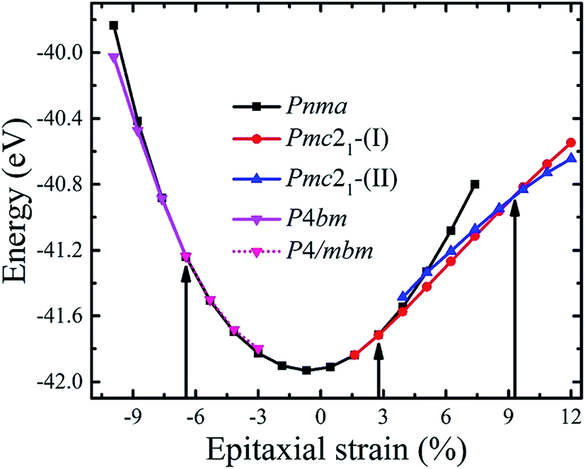 | ||
| Fig. 1 Computed total energies of the CsSnI3 films as a function of biaxial strain perpendicular to the [001] direction with geometries optimized to allow various distortions. The vertical lines mark the phase boundaries between different symmetries. At e = −6.49%, the P4bm phase transforms into the P4/mbm phase, as indicated by the pink short dotted line, though a second quantum order phase transition. | ||
As the strain varies from compression to tension, the ground state of the CsSnI3 films changes consecutively from the polar P4bm state to the non-polar Pnma state, then to the polar Pmc21-(I) state, followed by another polar Pmc21-(II) state. The structures of these phases are displayed in Fig. 2. Fig. 2a displays the structure of the P4bm state in which the Glazer notation is a0a0c+.41 The SnI6 octahedra rotate along the [001] direction in-phase (M2+ mode, Fig. S2,† called AFDzi). Besides the AFDzi, there is also an FE mode (Γ3−, called FEz) in the P4bm state. Fig. 2b displays the structure of the Pnma state which not only includes the AFDzi, but also AFDxy (tilts around an axis perpendicular to the (001), M5− mode, Fig. S2†), and its Glazer notion is a−a−c+. From the structure of Pmc21-(I) displayed in Fig. 2c, it can be seen that the rotations/tilts of the octahedra in this phase are similar with the Pnma state. Compared with the Pnma state, an FExy mode exists in the Pmc21-(I) phase. Fig. 2d displays the structure of another Pmc21 phase. Although it has same space group with the aforementioned Pmc21-(I) state, both of them have the FExy and AFDzi modes; however, the difference between Pmc21-(I) and Pmc21-(II) is that there is no AFDxy mode in the Pmc21-(II) phase. It is worth mentioning that compared with a previous study on the strain effect on CsSnI3 films, our study is more systematic.35 In our study, we not only consider a single factor such as octahedral rotation/tilt or off-center of the Sn cation, but also consider a combination of rotation/tilt and off-center. Therefore, we discovered the polar phase P4bm (compressive) and Pmc21-(I) (tensile) states. Thus, it is hoped that ferroelectricity can be found in other halide perovskites, such as CsBX3 (B = Ge, Sn and Pb; X = Cl, Br and I) under epitaxial strain.
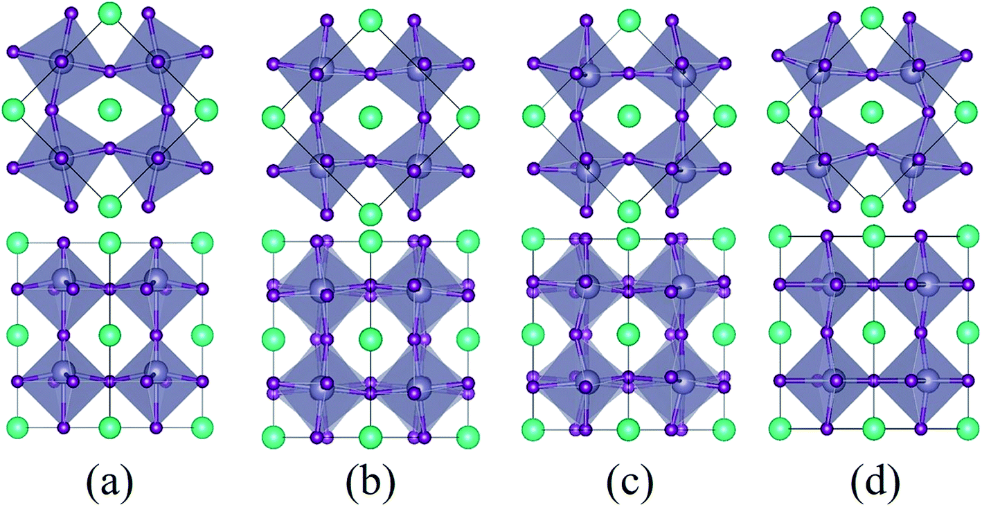 | ||
| Fig. 2 Model of the different epitaxial structures. Panels (a), (b) (c), and (d) display a schematic description of the P4bm, Pnma, Pmc21-(I), and Pmc21-(II) phases, respectively. The first layer represents polyhedral views of these phases from the c-axis, while the second layer is the view from the a and b-axes. The cyan, gray, and purple balls represent Cs, Sn and I atoms, respectively. | ||
For the polar P4bm state, its ground state occurs when e < −6.47%. It should be noted that the P4bm state will end up at the P4/mbm state when e is larger than −6.47% and this phase transformation is a second order quantum phase transition. First, taking the P4/mbm phase as the reference state, we calculated the electric polarization of this polar state. The calculated results are displayed in Fig. 3a, which shows that the calculated polarization monotonously decreases from 8.25 to 0.17 μC cm−2 as strain increases from −9.93% to −6.47%. Obviously, compared with a previous report on the inorganic perovskite (CsRb)Sn2I6, the calculated polarization is greatly enhanced.28 Especially, when strain is larger than −6.47%, the calculated value of polarization is close to zero. This confirms that the phase transition between the P4bm and P4/mbm phases is a second order transition. We then studied the electric structure of this phase. In Fig. 3b, the band gaps of the P4bm state are plotted as a function of the epitaxial strain, and to help understand the evolution of the electric structure of P4bm state, the results of the P4/mbm phase are also shown when e > −6.47% although it is not the ground state. In particular, the calculated band gaps first decrease from 0.52 to 0.00 eV (−9.93% > e > −5.31%), and then increase from 0.00 to 0.21 eV (−5.31% > e > −0.69%). Typically, standard exchange-correlation functionals such as GGA and LDA significantly underestimate the band gaps.42 Due to the importance of iodides in photovoltaic applications, it is essential to compute the electric structure of the strained CsSnI3 films as accurately as possible, especially the energy band gaps. Thus, the HSE06 functional was also selected in these calculations. The calculated results are displayed in Fig. 3b. The calculated band gaps increase compared with that from the PBEsol method and they have a similar trend vs. strain increasing. The semiconducting band gaps indicate that this FE state is not suitable for absorption in the solar spectrum. In addition, we plotted the band-structure of the P4bm state at e = −7.62%, and the results are displayed in Fig. 3c (PBEsol method) and Fig. 3d (HSE06 functional). It can clearly be seen that in the valence band of the P4bm state, the valence band maximum (VBM) is located at the Γ point of the Brillouin zone, while the conduction band minimum (CBM) does not lie at Γ point, thus, it possesses indirect band gaps. Indirect band gaps are unfavorable for light absorption. Nevertheless, Yu and Zunger previously highlighted an indirect band gap that did not result in weak absorption, and provided a direct allowed transition existing only at higher energy.43 Interestingly, after carefully studying the character of this band-structure, we find that there is band inversion (see Fig. S3†) at the Γ point, which has been reported in topological insulators. Such phenomenon has been discussed in previous reports on other halide perovskites.44,45 Thus, this property allows compressive CsSnI3 thin films to have potential application in the search for new bulk topological insulators.
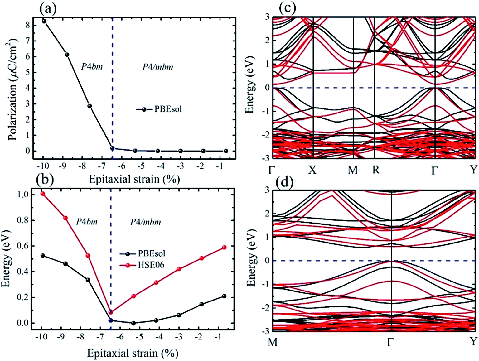 | ||
| Fig. 3 Electric polarization and electronic properties of the P4bm phase versus epitaxial strain. (a) Electric polarization. (b) Band gaps. (c and d) Band structures of the P4bm and P4/mbm phases calculated using the PBEsol and HSE06 functionals, respectively. The blue dashed lines in (a) and (b) represent the phase boundary of the P4bm and P4/mbm phases. The black lines in (c) and (d) represent the band structure of the P4bm phase at e = −7.62%, while the red lines represent the P4/mbm phase at e = −1.85%. The Fermi level is set at 0 eV and is indicated by the blue dashed line. | ||
We now focus on the strain e lying in the region between −0.47% and +1.62%. In this range, the computed ground state is the Pnma state (see Fig. 2). This state is centrosymmetrical in structure, thus it does not possess electric polarization. As the strain increases from −6.47% to +1.62%, the band gaps change from 0.00 to 0.42 eV within the PBEsol method (0.15 to 0.84 eV within the HSE06 method, see Fig. S4†). Moreover, there is a kink in the band gaps curves at e = −0.69%, because the epitaxial strain breaks the 3-fold degeneracy of the I-5p states, which has been discussed in a previous report.45 Similarly to the bulk state, both the VBM and CBM are located at the Γ point of the Brillouin zone, thus direct band gaps exist (Fig. S4†).
In the region of +1.67% < e < +9.30%, a polar phase named Pmc21-(I), which takes the place of the Pnma state, becomes the ground state. This phase has been also reported in other perovskite oxide compounds under tensile strain, such as BiFeO3 and SrZrO3.46,47 It is notable that the phase transition between the Pnma and Pmc21-(I) states is also a second order quantum transformation which is similar with the phase transition between the P4bm and P4/mbm phases. The calculated polarization of the strained CsSnI3 films is displayed in Fig. 4a. It can be seen that as the tensile strain increases from +1.61% to +9.30%, the polarization increases monotonically from 0.00 to 13.60 μC cm−2. The polarization value is significantly enhanced compared with that in previous reports on inorganic perovskite ferroelectrics and is the same order of magnitude with organic halide perovskite ferroelectrics such as CH3NH3GeI3.19,28 To confirm that the ferroelectricity of the Pmc21-(I) phase can be switched by an epitaxial electric field, we calculated the FE double well at e = +3.93% and the result is displayed in Fig. 4b. In addition, the FE double well gives the energy difference (ΔEh) between the ground-state FE structure and the high-symmetry paraelectric reference, which can be used to estimate the stability of polarization. According to the calculated ΔEh, we estimated the Curie temperature of the ferroelectricity and the calculated results are plotted in Fig. 4c (in the calculation, we take the ΔEh of BaTiO3 as a reference). The curve shows that the Curie temperature increases as the strain increases. Especially, it can clearly be seen that when the strain exceeds 6%, the calculated temperature is well above room temperature. In Fig. 4d illustrates how the band gaps change as the epitaxial strain increases. With the increase in strain from +1.61% to +9.30%, the calculated band gaps increase from 0.42 eV to 1.41 eV (0.84 eV to 1.97 eV with the HSE06 functional) which are suitable for absorption in the solar spectrum. In addition, the band gap tenability of the strained CsSnI3 films is about 0.99 eV. Although the band gap tunability is smaller than that previously achieved for FE materials doped with inorganic ions in KNbO3 (2.50 eV),4 the tunable band gaps can be compared with other doped halide perovskite FE materials, such as (cyclohexylammonium)2PbBr4−4xI4x (x = 0–0.175) and (N-methylpyrrolidinium)3Sb2Cl9−9xB9x (x = 0–1).48 To obtain a better understanding of the electric structure of the Pmc21-(I) state, the band structures were calculated. The calculated results show that this state has a direct band gap (Fig. S5†).
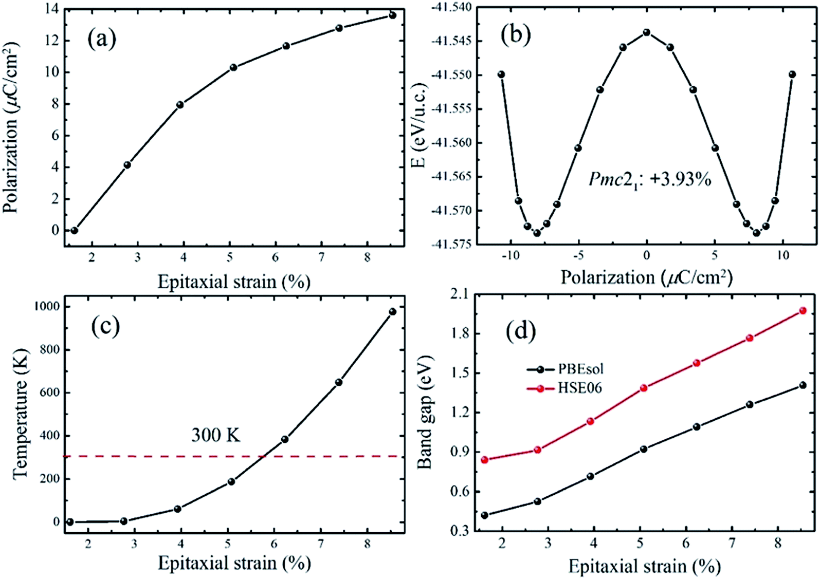 | ||
| Fig. 4 Electric polarization and electronic properties of the Pmc21-(I) phase versus epitaxial strain. (a) Electric polarization. (b) Double well of the Pmc21-(I) phase at e = +3.93%. (c) Estimated Curie temperature of the Pmc21-(I) phase. The red dashed line indicates 300 K. (d) Band gaps. | ||
Finally, when the tensile strain further increases (e > +9.30%), the Pmc21-(II) state is the ground state. Although it has same space group as the Pmc21-(I) phase, their lattice and electric structures are profoundly different. In addition to the difference in the rotation/tilt of the SnI6 octahedral in these two Pmc21 states, their lattice parameters are also significantly different. Generally, in a strained film, as the in-plane lattice constants increase, the out-of-plane lattice constants decrease. However, it is found that, at the phase boundary, there is significant jump for the c-lattice (0.497 Å, see Fig. S6†). In addition, the electric polarization value also has an obvious jump at e = +9.30% (6.09 μC cm−2). To lower the order in the fields, the energy of the phase with larger polarization will be lowered relative to a phase with smaller polarization by ![[P with combining right harpoon above (vector)]](https://www.rsc.org/images/entities/i_char_0050_20d1.gif) ·
·![[E with combining right harpoon above (vector)]](https://www.rsc.org/images/entities/i_char_0045_20d1.gif) . Thus, for a system in the vicinity of the phase boundary, a large electric-elastic response is predicted as the result of the possibility of switching between two phases with quite different polarization, band gaps, and c-lattice parameters. In particular, the Pmc21-(II) state just at the phase boundary could be driven by an applied electric field to the Pmc21-(I) state with a downward jump in the c-lattice. In addition, the Pmc21-(II) state could also be driven into the Pmc21-(I) state by an applied uniaxial compressive stress with an upward jump in polarization.
. Thus, for a system in the vicinity of the phase boundary, a large electric-elastic response is predicted as the result of the possibility of switching between two phases with quite different polarization, band gaps, and c-lattice parameters. In particular, the Pmc21-(II) state just at the phase boundary could be driven by an applied electric field to the Pmc21-(I) state with a downward jump in the c-lattice. In addition, the Pmc21-(II) state could also be driven into the Pmc21-(I) state by an applied uniaxial compressive stress with an upward jump in polarization.
To obtain a better understanding of these results, we next calculated the atom-resolved density of states for each state using the PBEsol method (Fig. 5). In these four phases, we find that the bottom of the conduction band is primary Sn-5p states, whereas the top of the valance band consists primarily of an antibonding combination of Sn-5s and I-5p states for P4bm, Pnma, and Pmc21-(I) phases which is consistent with a previous study.28 Furthermore, there is hybridization among the Sn-5s, Sn-5p, and I-5p states throughout the valence and conduction bands. This indicates that the epitaxial strain onhase with smaller hase with smaller films does not modify the orbital character at the band edges for the P4bm, Pnma, and Pmc21-(I) phases, but instead affects the band gap through structural changes. However, for the Pmc21-(II) phase, we find that the top of the CBM primarily consists of Sn-5s states. This may be related with the increase in lattice parameters of the Pmc21-(II) phase which can weaken the hybridization between Sn-5s and I-5p below the Fermi energy. Finally, we find that the band gap, broken inversion system, and strongly hybridized Sn-5s and I-5p states enable P4bm (indirect band gap) and Pmc21-(I) (direct band gap) to have a direct p–p optical transition.49
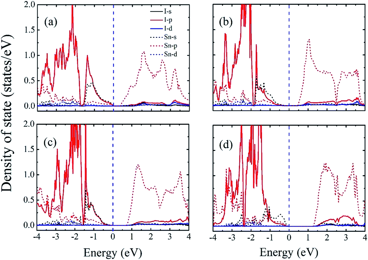 | ||
| Fig. 5 Atom-resolved density of states for (a) P4bm, (b) Pnma, (c) Pmc21-(I), and (d) Pmc21-(II) phases computed using the PBEsol method. The Fermi level is set at 0 eV and is indicated by the blue dashed line. | ||
4. Conclusion
In summary, we have comprehensively investigated the effects of biaxial strain and the accompanying structural distortions on the energy landscapes, electric polarization, and band gaps of films of the perovskite photovoltaic material CsSnI3 with first-principle calculations. It is found that both compressive and tensile strain can drive the non-polar phase (Pnma) to the polar phase (P4bm and Pmc21-(I)). Notably, our calculations show that the FE polarization is up to several μC cm−2 and that the polarization is considerably enhanced compared with previous studies. Unlike the nonpolar phase, the electric polarization present in these FE phases can effectively separate the photoexcited carriers, leading to novel FE photovoltaic materials with potentially enhanced energy conversion efficiency. Moreover, we show that compressive strain can induce a direct–indirect band gap transformation accompanied with a Pnma to P4bm transition. The Pmc21-(I) phase has a suitable direct band for visible light-harvesting and its band gaps can be altered by several tenths of an electronvolt under epitaxial tensile strain. In addition, we also predict that there is an electric-elastic response in the vicinity of the phase boundary of the Pmc21-(I) and Pmc21-(II) phases. It is expected that all-inorganic strained CsSnI3 films, which possess suitable band gap and large electric polarization, can be used as light-harvesting materials and epitaxial strain can be used as a new route to develop semiconductor FE materials that can promote the desirable separation of photo-excited carriers in the less-explored inorganic perovskite halide materials.Conflicts of interest
There are no conflicts to declare.Acknowledgements
This study has been supported by the National Natural Science Foundation of China though Grant No. 11604113. We also thank the High Performance Computing Center of Nanjing University for part of the numerical calculations.References
- A. Kojima, K. Teshima, Y. Shirai and T. Miyasaka, J. Am. Chem. Soc., 2009, 131, 6050–6051 CrossRef CAS PubMed.
- M. A. Green, A. Ho-Baillie and H. J. Snaith, Nat. Photonics, 2014, 8, 506–514 CrossRef CAS.
- K. T. Butler, J. M. Frost and A. Walsh, Energy Environ. Sci., 2015, 8, 838–848 CAS.
- I. Grinberg, D. V. West, M. Torres, G. Gou, D. M. Stein, L. Wu, G. Chen, E. M. Gallo, A. R. Akbashev, P. K. Davies, J. E. Spanier and A. M. Rappe, Nature, 2013, 503, 509–512 CrossRef CAS PubMed.
- J. E. Spanier, V. M. Fridkin, A. M. Rappe, A. R. Akbashev, A. Polemi, Y. Qi, Z. Gu, S. M. Young, C. J. Hawley, D. Imbrenda, G. Xiao, A. L. Bennett-Jackson and C. L. Johnson, Nat. Photonics, 2016, 10, 611–616 CrossRef CAS.
- R. Nechache, C. Harnagea, S. Li, L. Cardenas, W. Huang, J. Chakrabartty and F. Rosei, Nat. Photonics, 2015, 9, 61–67 CrossRef CAS.
- H. Borkar, V. Rao, M. Tomar, V. Gupta, J. F. Scott and A. Kumar, RSC Adv., 2017, 7, 12842–12855 RSC.
- W. Huang, C. Harnagea, D. Benetti, M. Chaker, F. Rosei and R. Nechache, J. Mater. Chem. A, 2017, 5, 10355–10364 CAS.
- J. Kreisel, M. Alexe and P. A. Thomas, Nat. Mater., 2012, 11, 260 CrossRef CAS PubMed.
- J. He, C. Franchini and J. M. Rondinelli, Chem. Mater., 2017, 29, 2445–2451 CrossRef CAS.
- Z. Fan, J. Xiao, K. Sun, L. Chen, Y. Hu, J. Ouyang, K. P. Ong, K. Zeng and J. Wang, J. Phys. Chem. Lett., 2015, 6, 1155–1161 CrossRef CAS PubMed.
- D. P. McMeekin, G. Sadoughi, W. Rehman, G. E. Eperon, M. Saliba, M. T. Hörantner, A. Haghighirad, N. Sakai, L. Korte, B. Rech, M. B. Johnston, L. M. Herz and H. J. Snaith, Science, 2016, 351, 151–155 CrossRef CAS PubMed.
- J. Burschka, N. Pellet, S.-J. Moon, R. Humphry-Baker, P. Gao, M. K. Nazeeruddin and M. Gratzel, Nature, 2013, 499, 316–319 CrossRef CAS PubMed.
- S. Liu, F. Zheng, N. Z. Koocher, H. Takenaka, F. Wang and A. M. Rappe, J. Phys. Chem. Lett., 2015, 6, 693–699 CrossRef CAS PubMed.
- W.-J. Yin, J.-H. Yang, J. Kang, Y. Yan and S.-H. Wei, J. Mater. Chem. A, 2015, 3, 8926–8942 CAS.
- A. Stroppa, C. Quarti, F. De Angelis and S. Picozzi, J. Phys. Chem. Lett., 2015, 6, 2223–2231 CrossRef CAS PubMed.
- J. M. Frost, K. T. Butler, F. Brivio, C. H. Hendon, M. van Schilfgaarde and A. Walsh, Nano Lett., 2014, 14, 2584–2590 CrossRef CAS PubMed.
- G. Sharada, P. Mahale, B. P. Kore, S. Mukherjee, M. S. Pavan, C. De, S. Ghara, A. Sundaresan, A. Pandey, T. N. Guru Row and D. D. Sarma, J. Phys. Chem. Lett., 2016, 7, 2412–2419 CrossRef PubMed.
- Y.-Q. Zhao, B. Liu, Z.-L. Yu, J. Ma, W. Qiang, P.-B. He and M.-Q. Cai, J. Mater. Chem. C, 2017, 5, 5356–5364 RSC.
- R. J. Sutton, G. E. Eperon, L. Miranda, E. S. Parrott, B. A. Kamino, J. B. Patel, M. T. Hörantner, M. B. Johnston, A. A. Haghighirad, D. T. Moore and H. J. Snaith, Adv. Energy Mater., 2016, 6, 1502458 CrossRef.
- C. Yi, J. Luo, S. Meloni, A. Boziki, N. Ashari-Astani, C. Gratzel, S. M. Zakeeruddin, U. Rothlisberger and M. Gratzel, Energy Environ. Sci., 2016, 9, 656–662 CAS.
- M. Kulbak, D. Cahen and G. Hodes, J. Phys. Chem. Lett., 2015, 6, 2452–2456 CrossRef CAS PubMed.
- Z. Li, M. Yang, J.-S. Park, S.-H. Wei, J. J. Berry and K. Zhu, Chem. Mater., 2016, 28, 284–292 CrossRef CAS.
- Y. S. Oh, X. Luo, F.-T. Huang, Y. Wang and S.-W. Cheong, Nat. Mater., 2015, 14, 407–413 CrossRef CAS PubMed.
- M. J. Pitcher, P. Mandal, M. S. Dyer, J. Alaria, P. Borisov, H. Niu, J. B. Claridge and M. J. Rosseinsky, Science, 2015, 347, 420–424 CrossRef CAS PubMed.
- N. A. Benedek and C. J. Fennie, Phys. Rev. Lett., 2011, 106, 107204 CrossRef PubMed.
- G. Song, G. Li, B. Gao, F. Liang and J. Zhang, J. Alloys Compd., 2017, 690, 923–929 CrossRef CAS.
- G. Gou, J. Young, X. Liu and J. M. Rondinelli, Inorg. Chem., 2017, 56, 26–32 CrossRef CAS PubMed.
- I. Chung, B. Lee, J. He, R. P. H. Chang and M. G. Kanatzidis, Nature, 2012, 485, 486–489 CrossRef CAS PubMed.
- I. Chung, J.-H. Song, J. Im, J. Androulakis, C. D. Malliakas, H. Li, A. J. Freeman, J. T. Kenney and M. G. Kanatzidis, J. Am. Chem. Soc., 2012, 134, 8579–8587 CrossRef CAS PubMed.
- K. P. Marshall, M. Walker, R. I. Walton and R. A. Hatton, Nat. Energy, 2016, 1, 16178 CrossRef CAS.
- J. P. Perdew, A. Ruzsinszky, G. I. Csonka, O. A. Vydrov, G. E. Scuseria, L. A. Constantin, X. Zhou and K. Burke, Phys. Rev. Lett., 2008, 100, 136406 CrossRef PubMed.
- G. Kresse and J. Hafner, Phys. Rev. B: Condens. Matter Mater. Phys., 1993, 47, 558–561 CrossRef CAS.
- P. E. Blöchl, Phys. Rev. B: Condens. Matter Mater. Phys., 1994, 50, 17953–17979 CrossRef.
- C. Grote and R. F. Berger, J. Phys. Chem. C, 2015, 119, 22832–22837 CAS.
- R. D. King-Smith and D. Vanderbilt, Phys. Rev. B: Condens. Matter Mater. Phys., 1994, 49, 5828–5844 CrossRef CAS.
- H. T. Stokes and D. M. Hatch, J. Appl. Crystallogr., 2005, 38, 237–238 CrossRef CAS.
- J. Heyd, G. E. Scuseria and M. Ernzerhof, J. Chem. Phys., 2003, 118, 8207–8215 CrossRef CAS.
- K. Momma and F. Izumi, J. Appl. Crystallogr., 2011, 44, 1272–1276 CrossRef CAS.
- S.-D. Guo and J.-L. Wang, RSC Adv., 2016, 6, 101552–101559 RSC.
- A. Glazer, Acta Crystallogr., 1972, 28, 3384–3392 CrossRef CAS.
- E. J. Baerends, O. V. Gritsenko and R. van Meer, Phys. Chem. Chem. Phys., 2013, 15, 16408–16425 RSC.
- L. Yu and A. Zunger, Phys. Rev. Lett., 2012, 108, 068701 CrossRef PubMed.
- S. Liu, Y. Kim, L. Z. Tan and A. M. Rappe, Nano Lett., 2016, 16, 1663–1668 CrossRef CAS PubMed.
- S. Chadov, X. Qi, J. Kübler, G. H. Fecher, C. Felser and S. C. Zhang, Nat. Mater., 2010, 9, 541–545 CrossRef CAS PubMed.
- H. Tian, A.-J. Mao, H. J. Zhao, Y. Cui, H. Li and X.-Y. Kuang, Phys. Chem. Chem. Phys., 2016, 18, 7680–7687 RSC.
- Y. Yang, W. Ren, M. Stengel, X. H. Yan and L. Bellaiche, Phys. Rev. Lett., 2012, 109, 057602 CrossRef PubMed.
- C. Ji, Z. Sun, A. Zeb, S. Liu, J. Zhang, M. Hong and J. Luo, J. Phys. Chem. Lett., 2017, 8, 2012–2018 CrossRef CAS PubMed.
- W.-J. Yin, T. Shi and Y. Yan, Adv. Mater., 2014, 26, 4653–4658 CrossRef CAS PubMed.
Footnote |
| † Electronic supplementary information (ESI) available. See DOI: 10.1039/c7ra07735a |
| This journal is © The Royal Society of Chemistry 2017 |