
 Open Access Article
 This Open Access Article is licensed under a Creative Commons Attribution-Non Commercial 3.0 Unported Licence
Modulating band gap of C4NP-h2D crystal nanoribbons and nanotubes under elastic strain
Shengqian Ma *a,
Weishun Mab,
Feng Lia,
Mei Zhua,
Jiguo Genga and
Min Lia
*a,
Weishun Mab,
Feng Lia,
Mei Zhua,
Jiguo Genga and
Min Lia
aSchool of Physics and Electronic Engineering, Taishan University, Taian, Shandong 271000, China. E-mail: shqma@ustc.edu.cn
bDepartment of Information Engineering, Laiwu Vocational and Technical College, Shandong 271100, China
First published on 22nd August 2017
Abstract
Using Density Functional Theory (DFT), band-gap modulation of C4NP-h2D nanoribbons and nanotubes under elastic strain is investigated in detail in this paper. The results indicate that the band gap of C4NP-h2D nanoribbons and nanotubes can be tuned in two ways, namely, stretching or compressing the nanoribbons and nanotubes whereby ε is changed from −10–10% in zigzag and armchair shapes, respectively. It was also revealed that the band gap of C4NP-h2D nanoribbons and nanotubes changes with increasing widths. Therefore, the C4NP-h2D nanoribbons and nanotubes are predicted to have great potential applications in strain sensor and optical electronics at the nanoscale.
1 Introduction
With in-depth study of low-dimensional materials,1,2 such as transition metal dichalcogenides,3–6 phosphorene oxide,7 elemental analogues of graphene: silicene, germanene, stanene, and phosphorene,8–13 arsenene, and antimonene,14 their unique properties and broad applications have attracted widespread interest. For example, the easily tuned band gap in semiconductor nanomaterials especially calls for a closer look at. Graphene is a semimetal with a zero band gap.15 BN nanosheet is a nonmagnetic wide-band-gap (∼6.0 eV) semiconductor.16–22 The atomically thin MoS2 is a new direct-gap (∼1.8 eV) semiconductor.23–25 Monolayer black phosphorus (phosphorene) is a direct bandgap (∼2.0 eV) semiconductor.26–28 To modulate the band gap of nanomaterials, many new nanomaterials have been effectively synthesized and studied in great detail.14,29–32 Atomically thin arsenene and antimonene are indirect semiconductors with band gaps of 2.49 and 2.28 eV, respectively. They can be transformed from indirect into direct band-gap semiconductors under small biaxial strain.16 GeCH3 is thermally stable up to 250 °C. It has a direct band gap of 1.69 eV, and gives strong photoluminescence emission.29 The band gap of GeCH3 nanoribbons is tuned under elastic strain.30 The MnPSe3 nanosheet is an antiferromagnetic semiconductor at its ground state, whereas both electron and hole doping induce its transition from antiferromagnetic semiconductor to ferromagnetic half-metal.31 The stability, electronic structures, and magnetic properties of single-walled C4N3 nanotubes have also been investigated.32 The nitrogenated holey two-dimensional structure C2N-h2D was successfully synthesized with a band gap of approximately 1.70 and 1.96 eV through DFT calculation and experimental measurements, respectively.33 The electronic properties of few-layer C2N-h2D are studied with different stacking orders and layer numbers.34In our work, because phosphene has excellent unique properties, and phosphorus and nitrogen belong to the same family. When the outer electrons and other atoms form covalent bonds, there is no dangling bond. The phosphorus atom is introduced to replace the nitrogen in the C2N-h2D structure, composition the analogous 2D C4NP-h2D sheet of 2D C2N-h2D sheet structure, which has a certain similar symmetry. The main point is that the nanoribbons and nanotubes are characterized through the change law of band gap by strain. We turned the analogous 2D C4NP-h2D sheets into two 1D nanostructures, namely, nanoribbons by cutting the sheet and nanotubes by rolling. Both nanostructures have typical topological shapes, zigzag and armchair. The band gaps of these nanostructures in either shape can be tuned through changing elastic strain and widths of the nanoribbons or radius of the nanotubes.
2 Computational details
We carried out first principles calculations based on Density Functional Theory (DFT) with Dmol3 package35,36 to study the geometric and electronic structures of C4NP-h2D nanosheets, nanoribbons, and nanotubes. The Perdew–Burke–Ernzerhof (PBE)37 functional of the generalized gradient approximation (GGA) was used to optimize the structures and achieve the primary electronic structures. The quadratic curve fitting was used to obtain the crystal structure with proper lattice constant. As is well known, weak interactions are out of the framework of standard PBE functional, so the DFT + D2 (D stands for dispersion) method was adopted with the Grimme vdW (van der Waals) correction38,39 to describe the weak interactions. The semi-core pseudopotential with double-numerical basis set plus d functions (DND) was adopted. Self-consistent field (SCF) calculations were performed with a convergence criterion of 10−6 a.u.40 The two adjacent nanoribbons were separated using a vacuum space of at least 15 Å to avoid interaction between layers. A K-point mesh of 1 × 1 × 9 or 1 × 1 × 15 grid was used for geometry optimization in armchair and zigzag nanoribbons or nanotubes, respectively. The orbital cutoff was set to be global and with a value of 4.2 Å. The atoms were relaxed without any symmetry constraints. Convergence in energy, force, and displacement was set at 1 × 10⁻⁵ Ha (1 Ha = 27.2114 eV), 0.002 Ha Å−1 and 0.005 Å, respectively.It is known that DFT always underestimates the band gap of the semiconductor. To address this issue, the Heyd–Scuseria–Ernzerhof (HSE)41 hybrid function correction, including screened Coulomb potential have been reported in many literatures.29,42,43 Literature44 explored the graphene nanoribbons under uniaxial elastic strain using GGA and HSE06 methods. The calculation results revealed that the trend of the band gap varying with strain is the same with the two methods. Therefore, in this paper we mainly study the variation of the band gap under widths and strains, while not emphasizing too much on the band gap accuracy.
3 Results and discussion
In our calculations, C4NP-h2D sheet was adopted to optimize the structure. Above all, A super cell with 18 atoms (C![[thin space (1/6-em)]](https://www.rsc.org/images/entities/char_2009.gif) :N:P = 4:1:1) was introduced (see Fig. 1(a)). After the structure of the minimum energy was achieved, the lattice parameter of super cell nanosheet was 8.695 Å, which fit a quadratic curve. Meanwhile, we calculated the frequency using MS and found that the structure did not have a virtual frequency. The band gap was 1.352 eV (see Fig. 1(b)). The in-plane covalent bond lengths of the C4NP-h2D were 1.423/1.468 Å for the C–C bond and 1.340/1.764 Å for the C–N/C–P bond. Compared to literature,33 the bond lengths increased by −0.006 Å/−0.002 Å for the C–C bond and 0.006/0.428 Å for the C–N/C–P bond. Obviously, when the P atoms were introduced, the length of C–P bond increased. Compared with the band gap of monolayer C2N-h2D sheet,33 the band gap of monolayer C4NP-h2D sheet decreased from 1.66 eV to 1.352 eV. This was mainly due to the closer overlap between the electron cloud of phosphorus and carbon, and the enhancement of gravity between each other. Meanwhile the biaxial elastic strains were introduced to the nanosheet. The strain is defined as ε = (d − d0)/d0, where d and d0 are the periodic length of C4NP-h2D nanoribbons with and without deformation, respectively. Stretching or compressing the nanosheet corresponds to a positive or negative value of ε, respectively. Fig. 1(c) indicates that the band gaps have a great change within our studied range of ε. The inset of Fig. 1(c) denotes the linear change of band gap with ε from −10–10%. The change shows a tendency to converge. However, when greater tensions are introduced, the band gaps increase again (see Fig. 1(c)). During the deformations course, the change in total energy of the system still follows the parabola change rule, indicating that the changes are within the elastic limit (see Fig. 1(d)). From these results, we can conclude that the C4NP-h2D nanosheet is a nonmagnetic narrow-band-gap semiconductor and the band gaps of system can be easily tuned.
:N:P = 4:1:1) was introduced (see Fig. 1(a)). After the structure of the minimum energy was achieved, the lattice parameter of super cell nanosheet was 8.695 Å, which fit a quadratic curve. Meanwhile, we calculated the frequency using MS and found that the structure did not have a virtual frequency. The band gap was 1.352 eV (see Fig. 1(b)). The in-plane covalent bond lengths of the C4NP-h2D were 1.423/1.468 Å for the C–C bond and 1.340/1.764 Å for the C–N/C–P bond. Compared to literature,33 the bond lengths increased by −0.006 Å/−0.002 Å for the C–C bond and 0.006/0.428 Å for the C–N/C–P bond. Obviously, when the P atoms were introduced, the length of C–P bond increased. Compared with the band gap of monolayer C2N-h2D sheet,33 the band gap of monolayer C4NP-h2D sheet decreased from 1.66 eV to 1.352 eV. This was mainly due to the closer overlap between the electron cloud of phosphorus and carbon, and the enhancement of gravity between each other. Meanwhile the biaxial elastic strains were introduced to the nanosheet. The strain is defined as ε = (d − d0)/d0, where d and d0 are the periodic length of C4NP-h2D nanoribbons with and without deformation, respectively. Stretching or compressing the nanosheet corresponds to a positive or negative value of ε, respectively. Fig. 1(c) indicates that the band gaps have a great change within our studied range of ε. The inset of Fig. 1(c) denotes the linear change of band gap with ε from −10–10%. The change shows a tendency to converge. However, when greater tensions are introduced, the band gaps increase again (see Fig. 1(c)). During the deformations course, the change in total energy of the system still follows the parabola change rule, indicating that the changes are within the elastic limit (see Fig. 1(d)). From these results, we can conclude that the C4NP-h2D nanosheet is a nonmagnetic narrow-band-gap semiconductor and the band gaps of system can be easily tuned.
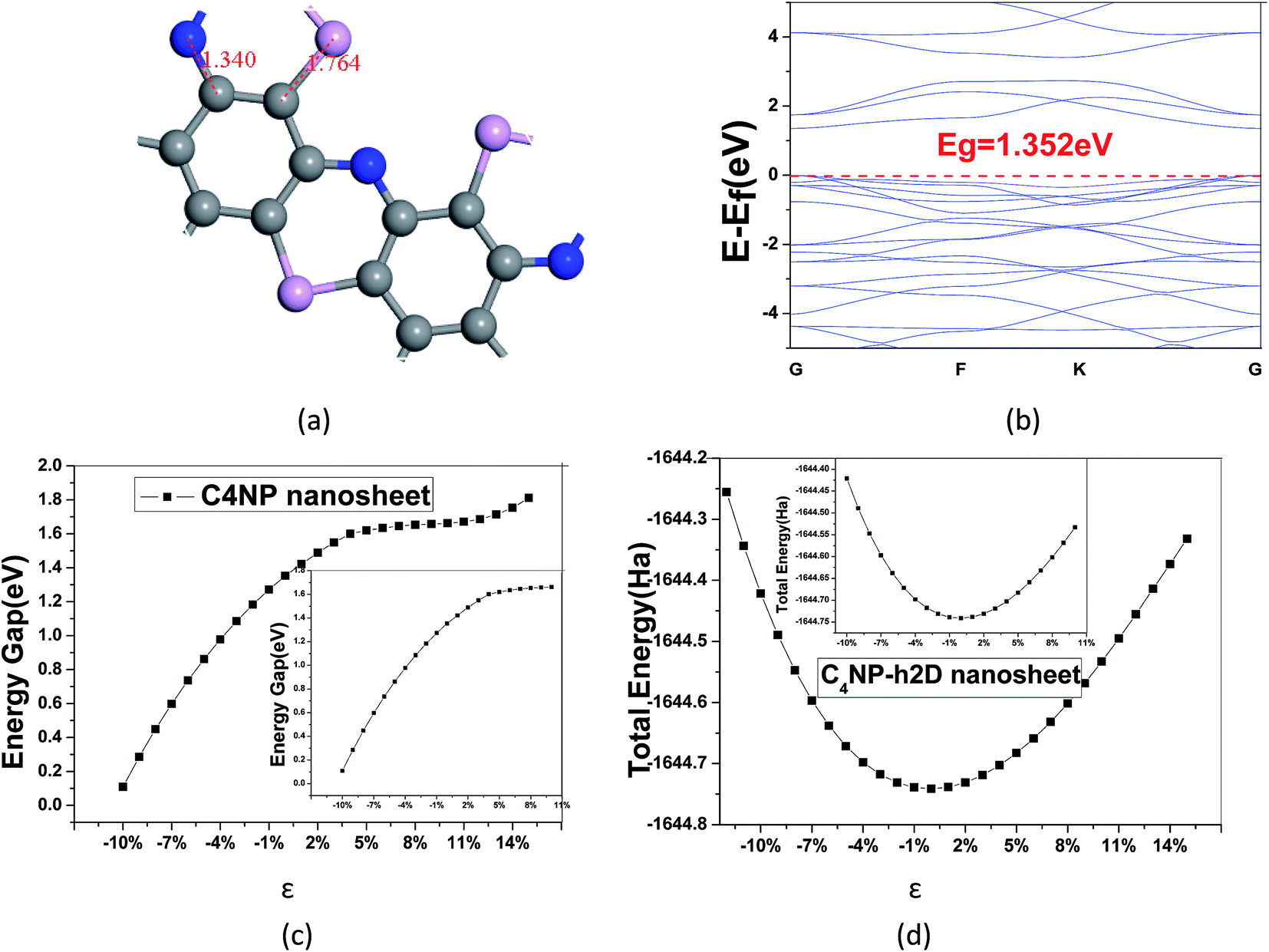 | ||
| Fig. 1 The optimized structures are plotted for (a) the super cell of the C4NP-h2D nanosheet, the blue, pink and gray balls represent nitride, phosphorus, and carbon atoms, respectively, (b) band structure of the super cell, (c) change of band gap with ε from −10–15% biaxial elastic strains (the right small picture denote change of band gap with ε from −10–10%), (d) the change of total energy with ε from −12% to −15% biaxial elastic strains (the up small picture denote the change of total energy with ε from −10% to −10%). | ||
Fig. 2 shows that phosphorus introduced play a significant role in structure parameters. Comparing Fig. 2(b) and (c), we can see that electronic cloud of phosphorus is larger. It disturbs the symmetry between N and P, and the polarization as well. Doping phosphorus effectively decreases the band gap of C2N–H2D nanosheet.
 | ||
| Fig. 2 (a) The optimized structures of the super cell of the C2N-h2D nanosheet with the blue and gray spheres representing nitride and carbon atoms, respectively. (b) and (c) depicts the electron density of the super cell of the C2N-h2D nanosheet and C4NP-h2D nanosheet, respectively. | ||
The center distance between two hexagonal holes in diamond nanosheet measures to be 8.695 Å. Compared with 8.30 Å in ref. 33, the center distance is increased by 0.395 Å (see Fig. 3(a)). The diamond nanosheet is cut into zigzag and armchair nanoribbons. The cutting edge appears to be dangling bonds. The C atoms at the edge of the C4NP-h2D nanoribbons are saturated with hydrogen (default). The two structures are selected as 3-zigzag and 2-armchair C4NP-h2D nanoribbons (see Fig. 3(b) and (c)). Their lengths are very close, 30.078 Å for 2-armchair and 30.998 Å for 3-zigzag, respectively. Through optimization, the center distance between two hexagonal holes is 8.684 Å and 15.254 Å for 3-zigzag and 2-armchair, respectively.
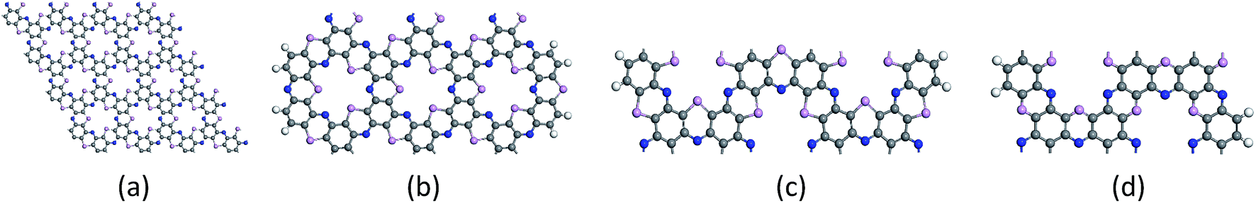 | ||
| Fig. 3 The optimized structures are plotted for (a) diamond of the C4NP-h2D nanosheet, (b) 3-zigzag, (c) 2-armchair and (d) 1.5-armchair C4NP-h2D nanoribbons, respectively. The blue, pink and gray spheres represent nitride, phosphorus, and carbon atoms, respectively. | ||
To modulate the band gap of C4NP-h2D nanoribbons, the uniaxial elastic strains along the ribbons' direction were introduced by stretching or compressing the nanoribbons. Fig. 4(a) shows that the band gap increases and then decreases when ε changes from −10–8% in both 3-zigzag and 2-armchair nanoribbons. Obviously, when ε is negative and decreases, the band gap decreases. When ε is positive and increases, the band gap decreases too. The band gap changes linearly with respect to ε and more rapidly when compressing the nanoribbons. Thus it can be seen that the band gap is sensitive to structural stress. Moreover, both stretching and compressing changes the band gap of 3-zigzag nanoribbons linearly with stress while compressing is more effective. In the course of stretching or compressing the nanoribbons, their energy change follows a parabolic curve with ε range from −10–8% (see Fig. 4(b) and (c)). In other words, the two structures are within the elastic limit. Hence the deformation shall not permanently alter the structure of nanoribbon. Fig. 4(d) and (e) shows the energy band changes with ε (ε = −10%, −5%, 0%, 5%, 8%). The energy band diagram reveals that the band gap is the biggest without deformation and that the band gap decreases in the course of deformation. Without strain, both the left and the right sides have a near linear relationship with changing ε. Similarly, we investigated the change of the band gap for armchair-shaped nanoribbons with varying width, (n = 1–5) (1.5-armchair (namely, 1.5a) nanoribbon see Fig. 3(d)) and zigzag-shaped C4NP-h2D nanoribbons with n = 1–14 (see Fig. 5(a) and (b)). The figures indicate that the band gap decreases with the increment of widths. These offered ways to modulate band gaps of nanomaterials, namely, by increasing or decreasing the strains, or increasing the widths.
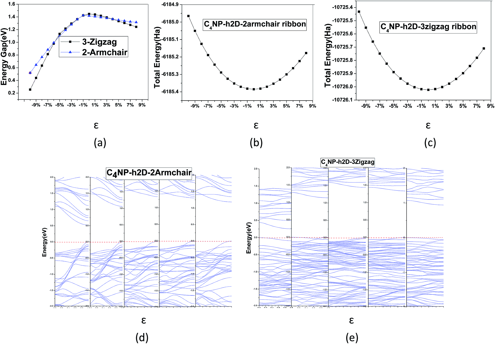 | ||
| Fig. 4 (a) Energy band gap with ε in 3-zigzag and 2-armchair. The total energy of (b) 2-armchair C4NP-h2D nanoribbons and (c) 3-zigzag C4NP-h2D nanoribbons with ε changing from −10–8%. The band structures of (d) 2-armchair and (e) 3-zigzag in C4NP-h2D nanoribbon with ε taking the values of −10%, −5%, 0%, 5% and 8%. | ||
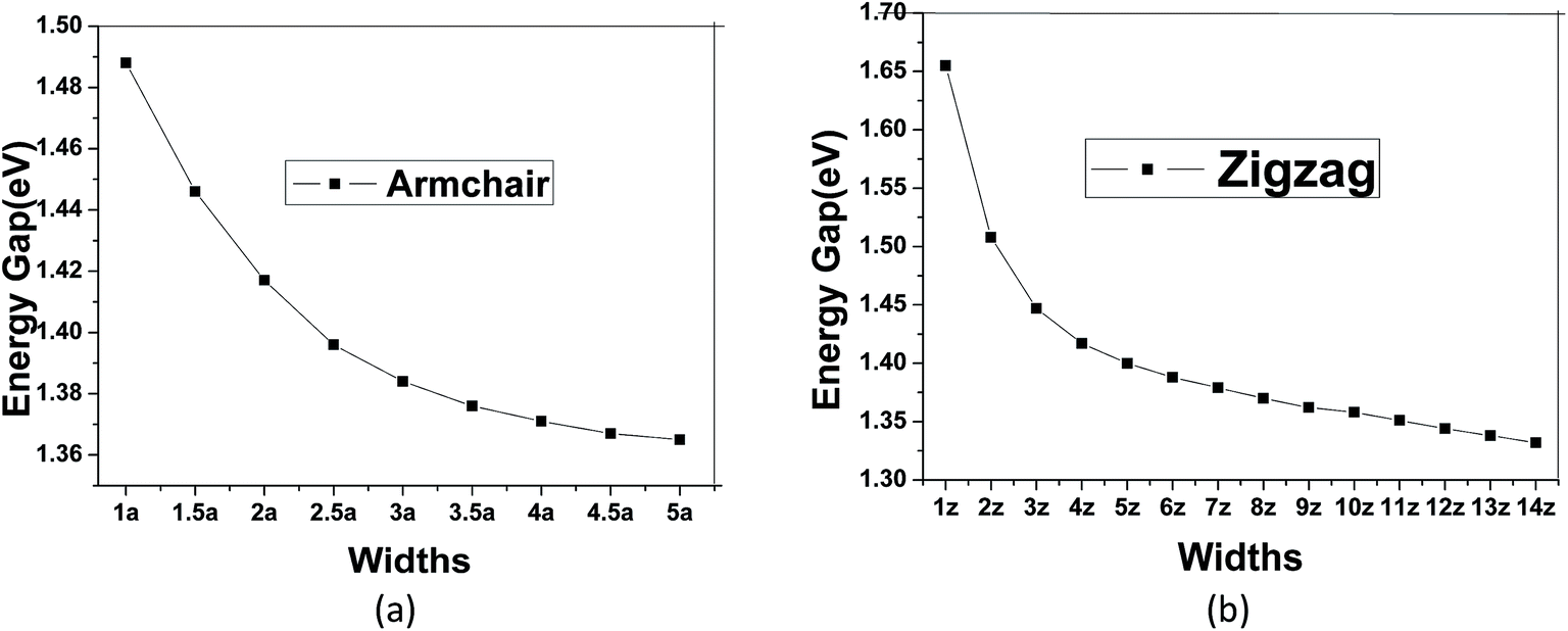 | ||
| Fig. 5 The changes of band gap with widths for armchair (1a–5a) (a) and zigzag (1z–14z) (b). | ||
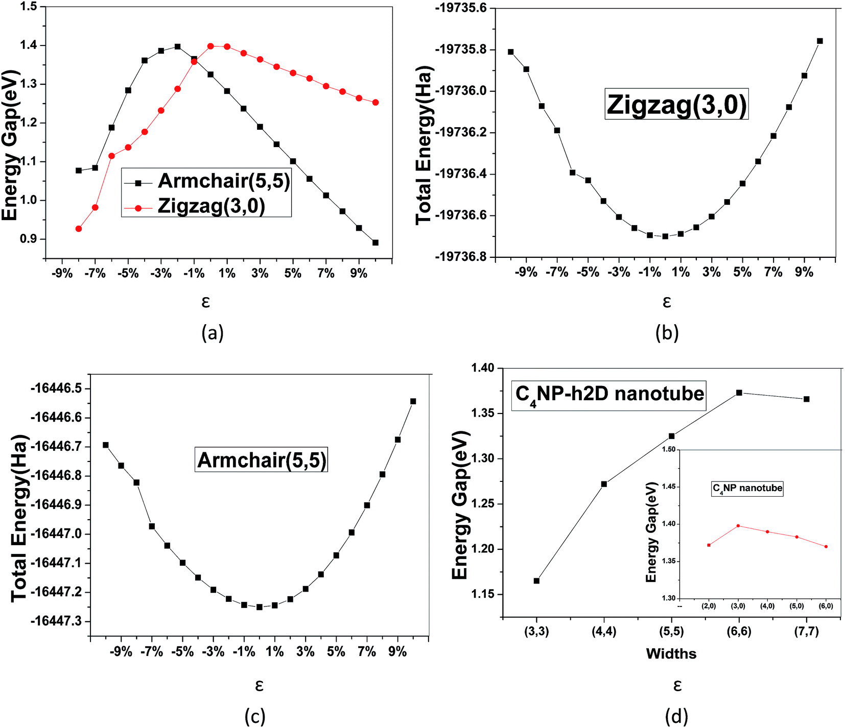
The band gaps of nanotubes are also studied. The C4NP-h2D nanosheets were rolled into nanotubes and then fully relaxed without placing constraint on any atomic positions (see Fig. 6). The zigzag (3,0) and armchair (5,5) C4NP-h2D nanotubes were adopted. Radii of the two structures were 7.331 Å and 7.377 Å, respectively. We appended a period along the axial direction of C4NP-h2D nanotubes and optimized the two structures. With a polynomial curve fitting, the structure of maximum energy was achieved. After obtaining the two structures, we investigated how the band gap changes with strain ε varying from −8% to 10% along the axial direction or the extension direction of nanotubes. Fig. 7(a) illustrates that the change of the band gap increases and then reduces with ε varying from −8% to 10%. Under compression, the band gap of the two structures is nearly linear with respect to ε. But in the case of tension, the change of band gap in armchair is a typical linear change. Hence one can see that band gap of armchair can be easily modulated. We then inspected the energy change with ε varying from −10–10%. Fig. 7(b) and (c) shows the armchair (5,5) and zigzag (3,0) nanotube are within the scope of the elastic limit. The band gaps change with radius (ESI Fig. 7(d)). The armchair showed a significant change, while the zigzag showed little change, leading to the conclusion that the band gap of armchair nanotube can be easily tuned.
 | ||
| Fig. 6 (a) C4NP-h2D sheet, (b) armchair (5,5) and (c) zigzag (3,0) SWCNPNTs are plotted. The blue, pink and gray spheres represent nitride, phosphorus and carbon atoms, respectively. | ||
 | ||
| Fig. 7 (a) Energy band gap with ε in armchair (5,5) and zigzag (3,0). The total energy of (b) armchair (5,5) and (c) zigzag (3,0) change with ε. (d) The changes of band gap with radius for armchair and zigzag (the right small figure). | ||
4 Conclusion
In summary, the band-gap modulation of C4NP-h2D nanoribbons and nanotubes has been studied under elastic strain with DFT. The band gap can be tuned by introducing tensile or compressional strains. Both ways are effective to modulate the band gap to a certain value. The results denominate that the band gap of C4NP-h2D nanoribbons and nanotubes can be tuned along two directions, namely, stretching or compressing ribbons and nanotubes when ε change from −10–10% in zigzag and armchair nanoribbons and nanotubes, respectively. The armchair nanoribbons and nanotubes can be easily modulated. Meanwhile, the band gap of the C4NP-h2D nanoribbons or nanotubes change with the increment of widths or radius. Therefore, the C4NP-h2D nanoribbons and nanotubes are narrow-band-gap nonmagnetic semiconductors. This property endows them great potential in applications in strain sensor and optical electronics at nanoscale.Compliance with ethical standards
This study was not funded.Conflicts of interest
The authors declare no conflicts of interest.Acknowledgements
The numerical calculations in this paper were executed on the computing system in the Computing Center of School of Physics and Electronic Engineering of Taishan University of China.References
- M. Peplow, Materials science: The hole story, Nature, 2015, 520, 148–150 CrossRef CAS PubMed.
- B. Dubertret, T. Heine and M. Terrones, The Rise of Two-Dimensional Materials, Acc. Chem. Res., 2015, 48(1), 1–2 CrossRef CAS PubMed.
- M. Chhowalla, Z. Liu and H. Zhang, Two-dimensional transition metal dichalcogenide (TMD) nanosheets, Chem. Soc. Rev., 2015, 44, 2584–2586 RSC.
- A. H. Loo, A. Bonanni, Z. Sofer and M. Pumera, Exfoliated transition metal dichalcogenides (MoS2, MoSe2, WS2, WSe2): An electrochemical impedance spectroscopic investigation, Electrochem. Commun., 2015, 50, 39–42 CrossRef CAS.
- S. X. Yang, C. Wang, H. Sahin, H. Chen, Y. Li and S. S. Li, et al., Tuning the Optical, Magnetic, and Electrical Properties of ReSe2 by Nanoscale Strain Engineering, Nano Lett., 2015, 15(3), 1660–1666 CrossRef CAS PubMed.
- T. Brumme, M. Calandra and F. Mauri, First-principles theory of field-effect doping in transition-metal dichalcogenides: Structural properties, electronic structure, Hall coefficient, and electrical conductivity, Phys. Rev. B: Condens. Matter Mater. Phys., 2015, 91, 155436 CrossRef.
- G. X. Wang, R. Pandey and S. P. Karna, Group-V elemental monolayers: the case of antimonene, Nanoscale, 2015, 7, 524–531 RSC.
- S. Balendhran, S. Walia, H. Nili, S. Sriram and M. Bhaskaran, Graphene Analogues: Elemental Analogues of Graphene: Silicene, Germanene, Stanene, and Phosphorene, Small, 2015, 11(6), 640–652 CrossRef CAS PubMed.
- H. Liu, A. T. Neal, Z. Zhu, D. Tomanek and P. D. Ye, Phosphorene: An Unexplored 2D Semiconductor with a High Hole Mobility, ACS Nano, 2014, 8, 4033–4041 CrossRef CAS PubMed.
- F. N. Xia, H. Wang and Y. C. Jia, Rediscovering Black Phosphorus as an Anisotropic Layered Material for Optoelectronics and Electronics, Nat. Commun., 2014, 5, 4458 CAS.
- Q. Tang and Z. Zhou, Graphene-analogous Low-dimensional Materials, Prog. Mater. Sci., 2013, 58, 1244–1315 CrossRef CAS.
- H. Oughaddou, H. Enriquez, M. R. Tchalala, H. Yildirim, A. J. Mayne and A. Bendounan, et al., Silicene, A Promising New 2D Material, Prog. Surf. Sci., 2015, 90, 46–83 CrossRef CAS.
- N. Takagi, C. L. Lin, K. Kawahara, E. Minamitani, N. Tsukahara, M. Kawai and R. Arafune, Silicene on Ag(1 1 1): Geometric and Electronic Structures of a New Honeycomb Material of Si, Prog. Surf. Sci., 2015, 90, 1–20 CrossRef CAS.
- S. L. Zhang, Z. Yan, Y. F. Li, Z. F. Chen and H. B. Zeng, Atomically Thin Arsenene and Antimonene: Semimetal–Semiconductor and Indirect–Direct Band-Gap Transitions, Angew. Chem., Int. Ed., 2015, 54, 3112–3115 CrossRef CAS PubMed.
- A. K. Geim and K. S. Novoselov, The Rise of Graphene, Nat. Mater., 2007, 6, 183–191 CrossRef CAS PubMed.
- K. Watanabe, T. Taniguchi, T. Niiyama, K. Miya and M. Taniguchi, Far-ultraviolet Plane-emission Handheld Device Based on Hexagonal Boron Nitride, Nat. Photonics, 2009, 3, 591–594 CrossRef CAS.
- X. L. Li, X. J. Wu, X. C. Zeng and J. L. Yang, Band-Gap Engineering via Tailored Line Defects in Boron-Nitride Nanoribbons, Sheets, and Nanotubes, ACS Nano, 2012, 6(5), 4104–4112 CrossRef CAS PubMed.
- D. Golberg, Y. Bando, Y. Huang, T. Terao, M. Mitome and C. Tang, et al., Boron Nitride Nanotubes and Nanosheets, ACS Nano, 2010, 4(6), 2979–2993 CrossRef CAS PubMed.
- S. Q. Ma, Electric structure and H2 adsorption properties of intrinsic and decorated h-ScN sheet by density functional theory, Appl. Surf. Sci., 2015, 347, 880–882 CrossRef CAS.
- E. Kan, H. Ren, F. Wu, Z. Li, R. Lu and C. Xiao, et al., Why the Band Gap of Graphene is Tunable on Hexagonal Boron Nitride, J. Phys. Chem. C, 2012, 116, 3142–3146 CAS.
- S. Q. Ma, Bandgap modulation and hydrogen storage with Cr-doped BN sheets, Int. J. Mod. Phys. B, 2015, 29(0), 1550160 CrossRef CAS.
- Y. Xie, Y. Luo and S. Liu, The Effects of the Uniaxial Pressure on Electronic Structures of the (6, 6) Single-walled Carbon Nanotube Crystal, Acta Phys. Sin., 2008, 57(7), 4364–4370 Search PubMed.
- B. Radisavljevic, A. Radenovic, J. Brivio, V. Giacometti and A. Kis, Single-layer MoS2 Transistors, Nat. Nanotechnol., 2011, 6, 147–150 CrossRef CAS PubMed.
- K. F. Mak, C. Lee, J. Hone, J. Shan and T. F. Heinz, Atomically Thin MoS2: A New Direct-Gap Semiconductor, Phys. Rev. Lett., 2010, 105, 136805 CrossRef PubMed.
- W. Zan, W. Geng, H. Liu and X. Yao, Electric-field and Strain-tunable Electronic Properties of MoS2/h-BN/Graphene Vertical Heterostructures, Phys. Chem. Chem. Phys., 2016, 18, 3159–3164 RSC.
- L. Li, Y. Yu, G. J. Ye, Q. Ge, X. Ou and H. Wu, et al., Black Phosphorus Field-effect Transistors, Nat. Nanotechnol., 2014, 9, 372–377 CrossRef CAS PubMed.
- Y. Takao, H. Asahina and A. Morita, Electronic Structure of Black Phosphorus in Tight Binding Approach, J. Phys. Soc. Jpn., 1981, 50, 3362–3369 CrossRef CAS.
- Y. Cai, G. Zhang and Y. W. Zhang, The Electronic Properties of Phosphorene/Graphene and Phosphorene/Hexagonal Boron Nitride Heterostructures, J. Phys. Chem. C, 2015, 119(24), 13929–13936 CAS.
- S. Jiang, S. Butler, E. Bianco, O. D. Restrepo, W. Windl and J. E. Goldberger, Improving the Stability and Optical Properties of Germanane via One-step Covalent Methyl-termination, Nat. Commun., 2014, 5, 3389 Search PubMed.
- S. Ma, F. Li and C. Jiang, Band-Gap Modulation of GeCH3 Nanoribbons Under Elastic Strain: A Density Functional Theory Study, J. Electron. Mater., 2016, 45, 5412 CrossRef CAS.
- X. X. Li, X. J. Wu and J. L. Yang, Half-Metallicity in MnPSe3 Exfoliated Nanosheet with Carrier Doping, J. Am. Chem. Soc., 2014, 136(31), 11065–11069 CrossRef CAS PubMed.
- Z. Guan, J. Wang, J. Huang, X. Wu, Q. Li and J. Yang, Metal-Free Magnetism and Half-Metallicity of Carbon Nitride Nanotubes: A First-Principles Study, J. Phys. Chem. C, 2014, 118, 22491–22498 CAS.
- J. Mahmood, E. K. Lee, M. Jung, D. Shin, I. Y. Jeon and S. M. Jung, et al., Nitrogenated Holey Two-dimensional Structures, Nat. Commun., 2015, 6, 1–7 Search PubMed.
- R. Zhang, B. Li and J. Yang, Effects of Stacking Order, Layer Number and External Electric Field on Electronic Structures of Few-layer C2N-h2D, Nanoscale, 2015, 7, 14062 RSC.
- B. Delley, An All-Electron Numerical Method for Solving the Local Density Functional for Polyatomic Molecules, J. Chem. Phys., 1990, 92, 508–517 CrossRef CAS.
- B. Delley, From Molecules to Solids with the DMol3 Approach, J. Chem. Phys., 2000, 113, 7756–7764 CrossRef CAS.
- J. P. Perdew, K. Burke and M. Ernzerhof, Generalized Gradient Approximation Made Simple, Phys. Rev. B: Condens. Matter Mater. Phys., 1996, 77, 3865 CAS.
- S. Grimme, Semiempirical GGA-Type Density Functional Constructed with a Long-Rang Dispersion Correction, J. Comput. Chem., 2006, 27, 1787–1799 CrossRef CAS PubMed.
- R. K. Ghosh, M. Brahma and S. Mahapatra, Germanane: A Low Effective Mass and High Bandgap 2-D Channel Material for Future FETs, IEEE Trans. Electron Devices, 2014, 61, 2309 CrossRef CAS.
- Y. Li and Z. Chen, Tuning Electronic Properties of Germanane Layers by External Electric Field and Biaxial Tensile Strain: A Computational Study, J. Phys. Chem. C, 2014, 118, 1148–1154 CAS.
- J. Heyd, G. E. Scuseria and M. Ernzerhof, Hybrid Functionals Based on A Screened Coulomb Potential, J. Chem. Phys., 2006, 124, 219906 CrossRef.
- L. Hu, J. Zhao and J. Yang, First Principles Study of Fluorine Substitution on Two-dimensional Germanane, J. Phys.: Condens. Matter, 2014, 26, 335302 CrossRef PubMed.
- Y. Ma, Y. Dai, W. Wei, B. Huang and M. H. Whangbo, Strain-induced Quantum Spin Hall Effect in Methyl-substituted Germanane GeCH3, Sci. Rep., 2014, 4, 7297 CrossRef CAS PubMed.
- Y. Zhang, X. Wu, Q. Li and J. Yang, Linear Band-Gap Modulation of Graphane Nanoribbons under Uniaxial Elastic Strain: A Density Functional Theory Study, J. Phys. Chem. C, 2012, 116(16), 9356–9359 CAS.
| This journal is © The Royal Society of Chemistry 2017 |