
 Open Access Article
 This Open Access Article is licensed under a Creative Commons Attribution-Non Commercial 3.0 Unported Licence
Ultra-high electrical conductivity and superior bendability simultaneously enabled in Ag nanowire based nanocomposites†
Minhong He‡
a,
Xinfang Gao‡b,
Bin Liub,
Jun Zhou*b and
Ziqi Liang *a
*a
aDepartment of Materials Science, Fudan University, Shanghai 200433, China. E-mail: zqliang@fudan.edu.cn
bCenter for Phononics and Thermal Energy Science, China-EU Joint Center for Nanophononics, Shanghai Key Laboratory of Special Artificial Microstructure Materials and Technology, School of Physics Science and Engineering, Tongji University, Shanghai 200092, China. E-mail: zhoujunzhou@tongji.edu.cn
First published on 14th September 2017
Abstract
Herein we report the solution fabrication of highly conductive and bendable conductors based on Ag nanowires (NWs) embedded within a polyvinylidene fluoride matrix. A typical percolation behavior of electrical conductivity is observed due to the formation of a conductive network. The highest conductivity, 1.77 × 10⁴ S cm−1, is achieved at 80 wt% Ag NWs and it remains nearly unchanged after 1000 bending events.
With rapid development of bendable and wearable electronics and sensors, there is a growing demand for flexible conductors,1,2 which play a significant role as interconnects or electrodes in a wide range of revolutionary functional devices ranging from roll-up displays,3,4 and wearable electronic equipment,5,6 to artificial and smart skin.7–11 Indeed, high mechanical strength and large electrical conductivity of conductors are required in these numerous applications.12–18 Promising candidates that meet the above requirements are nanocomposites with inorganic conductive fillers embedded in an organic matrix. In this regard, an effective electron pathway can be established by forming the network of fillers, while the matrix provides good mechanical properties. However, most of such nanocomposites suffer from poor electrical conductivity because of the limited filling fraction. A large fraction of conductive fillers would otherwise inevitably undermine the elasticity, deformability and processability of the resulting nanocomposites. For example, Xu and Zhu reported that the highest filling fraction of metal nanowires (NWs) were estimated to be less than ∼70 wt% in the nanocomposites based on polydimethylsiloxane (PDMS) matrix, showing the best conductivity of 8130 S cm−1.19 Above the upper limit fraction, the samples would be easily cracked when peeled off from the substrate and prone to wear and tear during practical operation. It is thus highly desirable to develop such nanocomposites that possess good conductivity and mechanical flexibility simultaneously.
It is straightforward to choose silver (Ag) as the conductive filler due to its excellent electrical conductivity and malleability.20,21 Several research groups have made the nanocomposites with Ag NWs dispersed in PDMS matrix. For instance, Huang et al. showed that Ag NWs were embedded into the PDMS interlayer and formed a sandwich structure, yielding an electrical conductivity as high as 1.52 × 10⁴ S cm−1.22 Park et al. prepared a conductive nanocomposite mat by coating Ag nanoparticles onto rubber fibres and acquired the highest conductivity of ∼5400 S cm−1 in the presence of large stretching deformation.23 These recent advances point to growing opportunities for highly conductive and flexible conductors based on Ag NWs with multi-layer structures in which the binding force between the layers is however poor, resulting in potential risk of damage after repeated bending.
In this work, we solution fabricated such nanocomposites that exhibited both superior electrical conductivity and excellent mechanical bending properties by dispersing Ag NWs uniformly into the polymeric matrix. Polyvinylidene fluoride (PVDF) was selected as the matrix material owing to its high temperature tolerance along with good thermal stability, plasticity, film-forming, mechanical strength and chemical resistance,24 which can be potentially applied to wearable electronic equipment.25 We made a range of nanocomposites with different filling fractions of Ag NWs and characterized their electrical conductivities and bendabilities, accordingly. At the content of 80 wt% Ag NWs in nanocomposites, the obtained conductivities are as high as 1.77 × 10⁴ S cm−1 which is among the best reported values and more importantly preserved with repeated bending cycles.
The Ag NWs/PVDF nanocomposites of several micrometres thick were attained by mixing Ag NWs and PVDF powders in dimethylformamide (DMF) solution and subsequently drying in aluminium molds within a N2-filled glovebox. The experimental details are described in ESI.† Their phase structures were inspected by X-ray diffraction (XRD) method. As shown in Fig. 1, the nanocomposites show strong diffraction peaks at 38.1, 44.3, 64.6 and 77.4 degrees, which correspond to the reflections from (111), (200), (220), and (311) planes of Ag crystal structure,26 respectively. These peaks are progressively enhanced in intensity when the mass fraction of Ag NWs increases from 5 wt% to 80 wt%. On the other hand, the absence of peaks at 32.8, 38.0, 54.8, and 65.4 degrees which are related to Ag2O suggest that the oxidization of Ag is prevented during the solution mixing process.
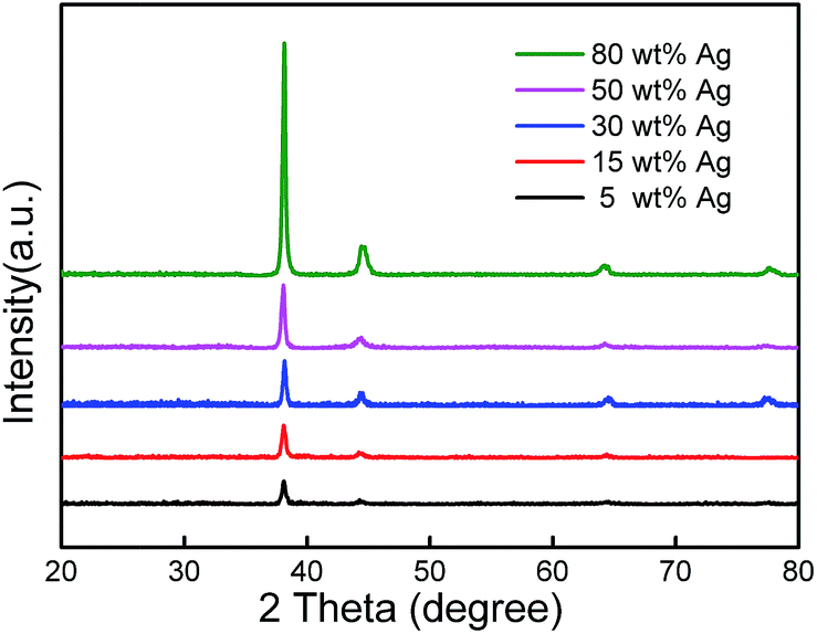 | ||
| Fig. 1 XRD patterns of Ag NWs/PVDF nanocomposites with different filling fractions. | ||
Typical photographs of as-fabricated Ag NWs/PVDF nanocomposite film are displayed in Fig. 2a, showing that the film is free-standing and has a smooth surface with an area of 4.1 cm2. Moreover, the film is easily bent without breaking. To quantify its superior bendability, the insets show photographs of a film inside a tube with a radius size of 4.7 mm, thus demonstrating its desired relevance for flexible and wearable modules. Field-emission scanning electron microscopy (FE-SEM) was further conducted to examine the morphology and nanostructures of the nanocomposites, and their typical top-view images are presented in Fig. 2b–f. It is clearly seen that Ag NWs are randomly distributed over the entire region of PVDF, in which the existence of high aspect ratio Ag NWs is evident and typical three-dimensional percolation networks are available dependent upon the filling fractions of Ag NWs.
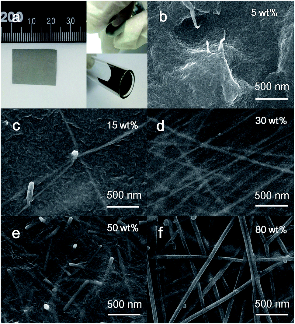 | ||
| Fig. 2 (a) Typical photographs of highly bendable Ag NWs/PVDF film. (b–f) Top-view SEM images of the nanocomposites with different filling fractions of Ag NWs. | ||
At a low filling fraction of 5 wt%, the majority of Ag NWs are isolated in nanocomposites as shown in Fig. 2b. As the fraction is increased to 15 wt%, a dense distribution of nanowire conjunctions is found while a connecting network is formed (Fig. 2c). This network is usually named as infinite cluster in percolation theory. Furthermore, such a network of Ag NWs in nanocomposites becomes more visible when the filling fraction continues to increase and the resulting electrical pathway is favourable for electron transport (Fig. 2d–f). It can be briefly concluded that with increasing filling fraction, more transport pathways are generated due to the presence of more conductive filler, which is advantageous for obtaining higher conductivity.
The filling fraction, distribution, aspect ratio and alignment of Ag NWs in nanocomposites would greatly affect electrical conductivity (σ). Fig. 3a shows the room-temperature σ dependences of Ag NWs/PVDF nanocomposite films on the filling fraction of Ag NWs. As shown in Fig. 3a and Table S1,† σ increases slowly from 3.68 × 10⁻⁶ S cm−1 at 5 wt% Ag NWs to 5.00 × 10² S cm−1 at 40 wt%, then significantly from 1.55 × 10³ S cm−1 at 50 wt% up to 1.77 × 10⁴ S cm−1 at 80 wt%. This phenomenon can be rationalized as the formation and expansion of infinite cluster of Ag NWs. Fig. 3c and d illustrate the electrical conduction mechanism within nanocomposite films with low and high filling fractions of Ag NWs, respectively. According to the percolation theory, when the volume fraction (ϕ) of Ag NWs is smaller than a critical value which is known as the critical volume fraction (ϕc), only isolated and finite clusters of Ag NWs exist in nanocomposites. Thus, electrons cannot transport from left to right side as shown in Fig. 3c. When ϕ is larger than ϕc, isolated clusters merged into a larger cluster, which is termed as infinite cluster in percolation theory. Therefore, electrons are able to transport from left to right side along a connected pathway as shown in Fig. 3d. Further increasing of ϕ raises the number of connected pathways which results in an increase of electrical conductivity.
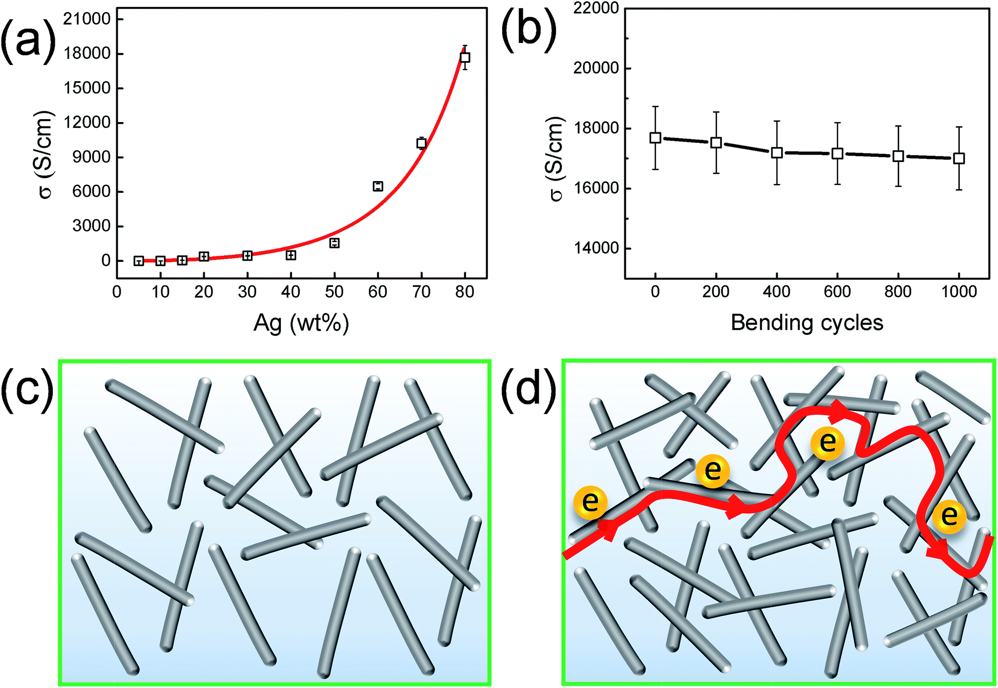 | ||
| Fig. 3 (a) Filling fraction dependences of electrical conductivity (σ) of the Ag NWs/PVDF nanocomposites. (b) Conductivity of the Ag NWs (80 wt%)/PVDF film versus the bending cycles from flat to a bending radius of 2.5 mm and back to flat. The points are experimental data and the fitted line in (a) is the corresponding numerical simulated results while the line in (b) is guideline. (c, d) Schematic illustrating the formation of conductive Ag NWs channel, which is dependent on the volume fraction of Ag NWs in nanocomposite films. A conductive pathway of Ag NWs is marked in red in (d). | ||
The σ values of nanocomposites can be fitted by using a phenomenological relation as shown in eqn (1) based on power law dependence where t is the exponent factor. The fitting shows ϕc = 0.28 vol% which corresponds to a filling fraction 1.63 wt%, and t = 2 in three-dimensional (3D) system.27 The fitted curves are in good agreement with the experimental results (as shown in Fig. 3a), thus providing strong evidence for the formation of a 3D percolation network, which favors electron transport. The aspect ratio of the Ag NWs is greater than 300 because the averaged diameter of NWs is 60 nm and the lengths of NWs are in the range of 20–80 μm. Based on these parameters, the numerical simulated ϕc is around 0.2 vol% by using the Monte-Carlo method,28 which is very close to the fitted value in eqn (1).
| σ ∝ (ϕ − ϕc)t | (1) |
In addition, we investigated the influence of mechanical bending on electrical conductivity of Ag NWs (80 wt%)/PVDF nanocomposite film. It is clearly seen from Fig. 3b that the conductivity of Ag NWs (80 wt%)/PVDF film remains little changed when bending to a radius of 2.5 mm and then releasing back to flat. With the increase of the number of bending events, conductivity decreased slightly, even after 1000 bending events, the ultra-high electrical conductivity of Ag NWs (80 wt%)/PVDF film is maintained constant with only ∼4% loss, indicating that the nanocomposite film possesses outstanding electrical conductivity and flexibility simultaneously.
Lastly, we demonstrated the application of such nanocomposite films for flexible conductors. We constructed a prototypic electrical circuit experiment by cutting as-fabricated Ag NWs (5–80 wt%)/PVDF films into a shape that is connected to the circuit, as shown in Fig. 4a–f. The samples with different filling fractions were connected while observing the changes of the diode luminance. It is found that when the filling fraction is 5 wt% (Fig. 4a), the diode is off, indicating that nanocomposites is almost insulator, consistent with the very low conductivity of 3.7 × 10⁻⁶ S cm−1 as shown in Fig. 3a. When the filling fraction continues to increase, the diode remains lit. It is explicitly seen from Fig. 4b–f that the luminance increases with the increasing filling fraction. This phenomenon confirms that as the filling fraction increases, a better conductive grid is formed and hence the conductivity is increased. At the highest fraction of 80 wt% Ag NWs, the composite film displays the brightest diode luminesce at the bending state, indicating its best conductivity (Fig. 4g).
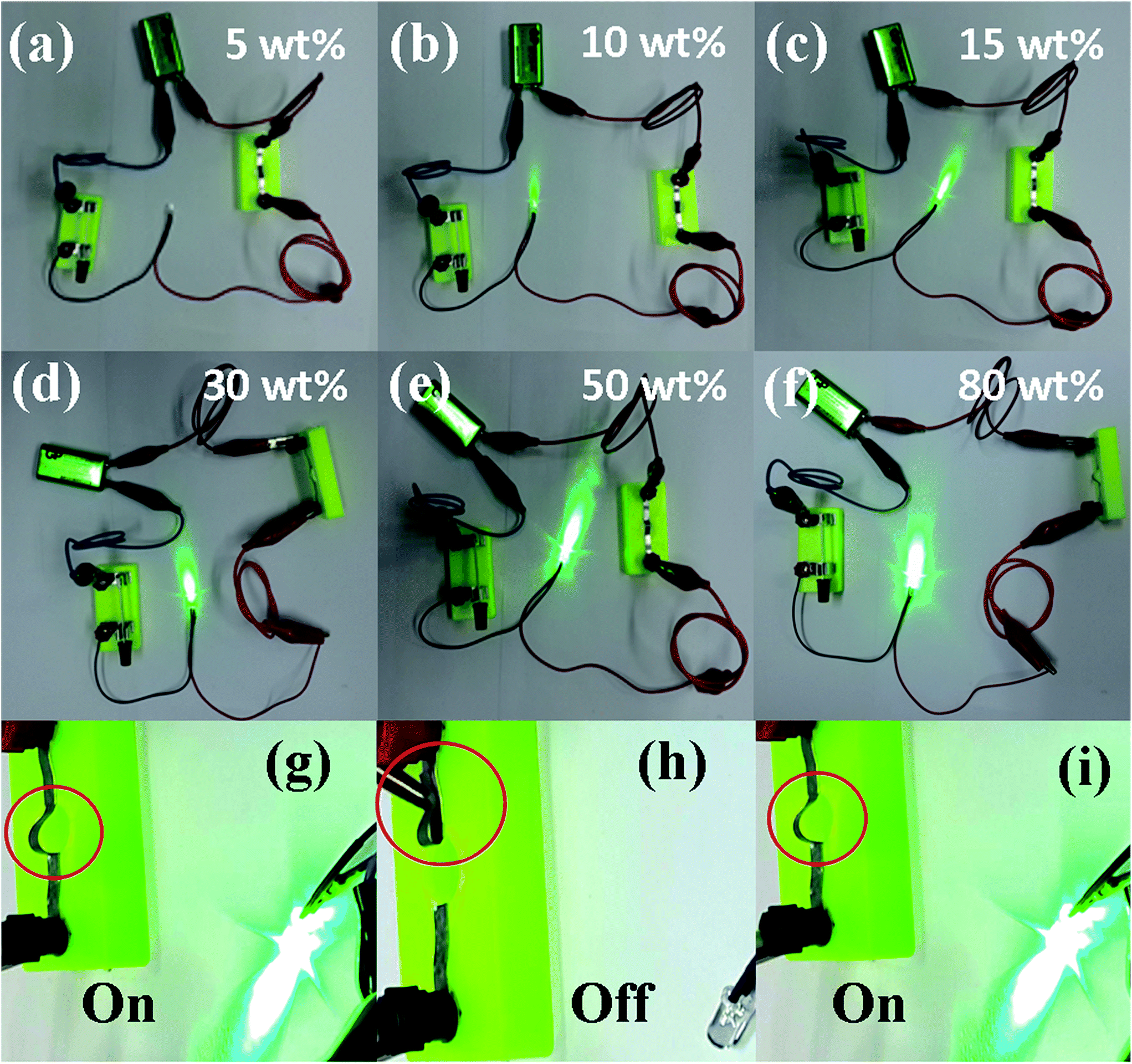 | ||
| Fig. 4 Demonstration experiments of the Ag NWs/PVDF nanocomposites. (a–f) With increasing filling fraction, the luminance of the diode is notably enhanced. (g–i) The maintained high conductivity, when bending, of the optimal Ag NWs (80 wt%)/PVDF film as indicated by red cycle. | ||
Also, we bended the film to control the diode by disconnecting and reconnecting the circuit. Fig. 4h and i and Movie S1 in the ESI† illustrate such processes of the Ag NWs (80 wt%)/PVDF film. Remarkably, the composite film presents excellent bendability and deformability while preserving good conductivity.
In conclusion, we have successfully fabricated ultra-highly conductive and flexible nanocomposites by homogeneously embedding Ag NWs network within PVDF matrix. A typical percolation behavior of electrical conductivity is observed due to the formation of conductive network. The critical volume fraction of percolation is found to be as low as 0.28 vol% which is in excellent agreement with the numerical simulation results. We also find that a quadratic dependence of electrical conductivity on ϕ − ϕc, which is consistent with the electrical percolation theory. When the filling fraction of Ag NWs is 80 wt%, an ultra-high electrical conductivity of 1.77 × 10⁴ S cm−1 is obtained, which is among the highest value of silver based composites.19,22,23 The samples show superior stability because the high electrical conductivity is almost unchanged after 1000 bending events. Therefore, our study demonstrates a promising fabrication method of highly conductive and flexible conductors for the potential applications of wearable electronic devices.
Conflicts of interest
There are no conflicts to declare.Acknowledgements
This work is sponsored by the National Natural Science Foundation of China (NSFC) under grant No. 51673044 (Z. L.). J. Z. acknowledges the support from the program for Professor of Special Appointment (Eastern Scholar) at Shanghai Institutions of Higher Learning (Grant No. TP2014012).References
- M. Melzer, J. I. Mönch, D. Makarov, Y. Zabila, G. S. C. Bermúdez, D. Karnaushenko, S. Baunack, F. Bahr, C. Yan, M. Kaltenbrunner and O. G. Schmidt, Adv. Mater., 2015, 27, 1274–1280 CrossRef CAS PubMed.
- W. Lin, S. Liu, T. Gong, Q. Zhao and W. Huang, Adv. Mater., 2014, 26, 570–606 CrossRef CAS PubMed.
- L. Zhou, A. Wanga, S. Wu, J. Sun, S. Park and T. N. Jackson, Appl. Phys. Lett., 2006, 88, 083502 CrossRef.
- S. Kim, H.-J. Kwon, S. Lee, H. Shim, Y. Chun, W. Choi, J. Kwack, D. Han, M.-S. Song, S. Kim, S. Mohannadi, I.-S. Kee and S. Y. Lee, Adv. Mater., 2011, 23, 3511–3516 CrossRef CAS PubMed.
- S. Chen, Z. Lou, D. Chen, K. Jiang and G. Shen, Adv. Mater. Technol., 2016, 1, 1600136 CrossRef.
- Q. Wu and J. Hu, Smart Mater. Struct., 2017, 26, 045037–045044 CrossRef.
- J. Ge, L. Sun, F. R. Zhang, Y. Zhang, L. A. Shi, H. Y. Zhao, H. W. Zhu, H. L. Jiang and S. H. Yu, Adv. Mater., 2016, 28, 722–728 CrossRef CAS PubMed.
- I. You, B. Kim, J. Park, K. Koh, S. Shin, S. Jung and U. Jeong, Adv. Mater., 2016, 28, 6359–6364 CrossRef CAS PubMed.
- M. Kaltenbrunner, T. Sekitani, J. Reeder, T. Yokota, K. Kuribara, T. Tokuhara, M. Drack, R. Schwodiauer, I. Graz, S. Bauer-Gogonea, S. Bauer and T. Someya, Nature, 2013, 499, 458–463 CrossRef CAS PubMed.
- J. Y. Sun, C. Keplinger, G. M. Whitesides and Z. Suo, Adv. Mater., 2014, 26, 7608–7614 CrossRef CAS PubMed.
- S. Park, H. Kim, M. Vosgueritchian, S. Cheon, H. Kim, J. H. Koo, T. R. Kim, S. Lee, G. Schwartz, H. Chang and Z. Bao, Adv. Mater., 2014, 26, 7324–7332 CrossRef CAS PubMed.
- Y. Hu, T. Zhao, P. Zhu, Y. Zhu, X. Shuai, X. Liang, R. Sun, D. D. Lu and C.-P. Wong, J. Mater. Chem. C, 2016, 4, 5839–5848 RSC.
- T. Cheng, Y. Zhang, W.-Y. Lai and W. Huang, Adv. Mater., 2015, 27, 3349–3376 CrossRef CAS PubMed.
- T. Q. Trung and N.-E. Lee, J. Mater. Chem. C, 2017, 5, 2202–2222 RSC.
- J. Liang, L. Li, K. Tong, Z. Ren, W. Hu, X. Niu, Y. Chen and Q. Pei, ACS Nano, 2014, 8, 1590–1600 CrossRef CAS PubMed.
- H. Wu, Y. A. Huang, F. Xu, Y. Duan and Z. Yin, Adv. Mater., 2016, 28, 9881–9919 CrossRef CAS PubMed.
- H. Lee, I. Kim, M. Kim and H. Lee, Nanoscale, 2016, 8, 1789–1822 RSC.
- Z. Yang, J. Deng, X. Sun, H. Li and H. Peng, Adv. Mater., 2014, 26, 2643–2647 CrossRef CAS PubMed.
- F. Xu and Y. Zhu, Adv. Mater., 2012, 24, 5117–5122 CrossRef CAS PubMed.
- M. Bharti, A. Singh, S. Samanta, A. K. Debnath, D. K. Aswal, K. P. Muthe and S. C. Gadkari, Energy Convers. Manage., 2017, 144, 143–152 CrossRef CAS.
- L. Hu, H. S. Kim, J.-Y. Lee, P. Peumans and Y. Cui, ACS Nano, 2010, 4, 2955–2963 CrossRef CAS PubMed.
- G.-W. Huang, H.-M. Xiao and S.-Y. Fu, Sci. Rep., 2015, 5, 13971 CrossRef PubMed.
- M. Park, J. Im, M. Shin, Y. Min, J. Park, H. Cho, S. Park, M.-B. Shim, S. Jeon, D.-Y. Chung, J. Bae, J. Park, U. Jeong and K. Kim, Nat. Nanotechnol., 2012, 7, 803–809 CrossRef CAS PubMed.
- C. Silvestre, D. Duraccio and S. Cimmino, J. Mater. Chem. A, 2017, 5, 10470–10479 Search PubMed.
- P. Martins, A. C. Lopes and S. Lanceros-Mendez, Prog. Polym. Sci., 2014, 39, 683–706 CrossRef CAS.
- J. Ma, K. Wang and M. Zhan, ACS Appl. Mater. Interfaces, 2015, 7, 16027–16039 CAS.
- N. Shenogina, S. Shenogin, L. Xue and P. Keblinski, Appl. Phys. Lett., 2005, 87, 133106 CrossRef.
- M. Foygel, R. D. Morris, D. Anez, S. French and V. L. Sobolev, Phys. Rev. B: Condens. Matter Mater. Phys., 2005, 71, 104201 CrossRef.
Footnotes |
| † Electronic supplementary information (ESI) available. See DOI: 10.1039/c7ra07714a |
| ‡ Authors contributed equally to this work. |
| This journal is © The Royal Society of Chemistry 2017 |