
 Open Access Article
 This Open Access Article is licensed under a
 Creative Commons Attribution 3.0 Unported Licence
Gate modulated and enhanced optoelectronic performance of MoSe2 and CVD-grown MoS2 heterojunctions
Yujue Yang a,
Nengjie Huoa and
Jingbo Li*ab
a,
Nengjie Huoa and
Jingbo Li*ab
aSchool of Materials and Energy, Guangdong University of Technology, Guangzhou 510006, P. R. China
bState Key Laboratory for Superlattices and Microstructures, Institute of Semiconductors, Chinese Academy of Sciences, Beijing 100083, P. R. China. E-mail: jbli@semi.ac.cn
First published on 22nd August 2017
Abstract
Van der Waals heterojunctions, stacked with different two-dimensional materials, have enabled novel optoelectronic functionalities with high performances for various applications such as in photodetectors, solar cells and light-emitting diodes. Herein, we fabricated MoSe2 and CVD-grown MoS2 heterojunctions with significant gate modulated photovoltaic effect with an open-circuit voltage of 0.16 V and power conversion efficiency of ∼0.5% due to the type-II band alignment and gate tunable band slope. Moreover, the photo-responsivity was dramatically improved to ∼350 A W−1, which is two orders of magnitude larger than that of the isolated components (MoSe2 or MoS2), and the temporal response was as fast as ∼10 ms at negative back gate. All these results indicate the vast potential applications of heterojunctions, with facile procedure, in photovoltaic cells and photodetectors.
Introduction
Two-dimensional (2D) transition metal dichalcogenides (TMDs) with sizable band gap have been demonstrated as promising candidates in the new generation of optoelectronics such as logic transistors, photodetectors and solar cells in the past decade.1–6 The key benefits include their unique and excellent properties such as atomically thin profile, mechanical flexibility, high mobility and strong light-matter interaction. Following great success, the van der Waals (vdW) heterostructures assembled with different 2D materials have recently emerged as a new artificial platform for novel optoelectronic applications.7–9 For example, graphene with h-BN or MoS2 based heterostructures have enabled the vertical field-effect transistors (VFETs) with a switching ratio higher than 1 × 10³ and high current density of up to 5000 A cm−2 (ref. 10) and have also performed remarkable multiple optoelectronic functions, including highly sensitive photodetection and gate-tunable photocurrent generation with a maximum internal quantum efficiency up to 85%.11,12 The MoS2/WSe2 PN heterojunctions can exhibit excellent current rectifying and photovoltaic as well as electroluminescence properties through strong interlayer coupling and tunnelling transport mechanism, suggesting a great application potential in solar cells and LEDs.7,8,13 These results suggest that the stacked vdW multi-heterostructures of layered materials can extend the applications of 2D material systems and open up new opportunities in future nano- and optoelectronic devices with high performance and large-scale integration.Herein, MoSe2 and CVD-grown MoS2 heterojunctions are stacked on SiO2/Si substrate to form 2D heterostructures with type-II band alignment. The CVD–MoS2 with large surface area is used to make the stacking procedure of the heterostructures easier by avoiding the operations through microscopic systems. The heterojunctions based transistors exhibit significant photovoltaic properties, which can be modulated by back gate due to the gate tunable band slope. Under negative gate, a significant open-circuit voltage (Voc) of 0.16 V and power conversion efficiency (PCE) of ∼0.5% was observed. Moreover, the photo-responsivity was improved up to ∼350 A W−1, which was about two orders of magnitude larger than that in isolated MoSe2 or MoS2. As a result, herein we propose a new platform to enhance the optoelectronic performance of heterojunctions based transistors that could supplement the unique 2D vdW heterojunction community for high performance and easy-processing of solar cells and photodetectors.
Experimental
CVD growth of MoS2
MoS2 was grown by chemical vapour deposition (CVD) on 285 nm SiO2/Si substrates. After consecutive cleaning by acetone, 2-propanol and DI-water, the substrates were placed face-down above a ceramic boat crucible containing ∼2 mg of MoO3 and loaded into a quartz tube furnace. CVD growth was performed at atmospheric pressure using ultra-high-purity nitrogen as the carrier gas. A second crucible containing ∼250 mg of sulfur was placed upstream from the growth substrates. The growth recipe is as follows: the system was purged with ultra-high-purity N2 gas with 500 sccm flow rate for 10 min and was heated up to 300 °C for 10 min with 100 sccm. It was then ramped to the growth temperature of 680 °C with 10 sccm of carrier gas flow. The temperature of 680 °C was then set for 10 min and cooled to room temperature naturally. During the cooling process, the carrier gas flow rate was maintained at 10 sccm. Below 550 °C, the flow was increased to 300 sccm and the furnace was also opened to attain faster cooling.Preparation of MoSe2/CVD-grown MoS2 heterostructures
First, the MoSe2 flakes were exfoliated on the SiO2/Si (90 nm-thick SiO2) substrates via micromechanical cleavage approach. Second, the Ti/Au electrodes were deposited using laser writing lithography and metal deposition technique. Note that one of the electrodes was separated from the MoSe2 flakes. Then, a 30 nm-thick insulating Al2O3 window was deposited to cover the electrodes that contacted with the flakes. Finally, the poly(methyl methacrylate)(PMMA) liquid was spin coated on the substrate with CVD grown MoS2 at a rotating speed of 4000 rps. After annealing at 150 °C for 30 min, the substrate with the PMMA film was soaked into 2 M NaOH solution. Then, the PMMA with the MoS2 film was floated and transferred onto another substrate to cover the MoSe2 device. Finally, the PMMA was dissolved in acetone to obtain the stacked MoSe2/MoS2 heterostructures.Device fabrication and characterization
Metal contacts were fabricated by laser writing lithography, and Ti (2 nm)/Au (50 nm) electrodes were evaporated by e-beam and thermal evaporation. Finally, the devices were annealed at 150 °C for 1 hour in a glove box to improve their contact quality. Al2O3 was deposited with the atomic layer deposition (ALD) technique (Savannah 200, Cambridge Nanotech). The temperature was maintained at 80 °C during the process of deposition. All the measurements were performed at ambient conditions using an Agilent B1500A semiconducting device analyzer. Responsivity and temporal response times were measured under short-pulsed light at a wavelength of 635 nm from a four-channel laser, controlled with an Agilent A33220A waveform generator.Results and discussion
The optical microscopy image and schematic of the devices are shown in Fig. 1a and b, respectively. Fig. 1c shows the Raman spectra of the heterojunctions and their components. The Raman peaks of the stacked heterostructures contain typical vibration modes of both MoSe2 and MoS2, indicating the formation of heterostructures. Fig. 1d shows the back gate dependence of drain current of the transistors with forward and backward gate scanning and also reveals their N-type behaviour with large hysteresis due to the defects in the materials. Under light illumination, the current is improved by three orders of magnitude in the depletion region, indicating sensitive photo-responsive property. The output characteristics of the heterojunctions for different back-gate voltage Vg under light illumination in log and linear scale are shown in Fig. 1e and the inset, respectively, and we can observe evident photovoltaic effect, which can be modulated by the back gate. Being control devices, no open-circuit voltage can be observed in isolated MoSe2 and MoS2, as shown in Fig. 1f and g, respectively. This reveals that the photovoltaic property originates from the stacking of MoS2 and MoSe2.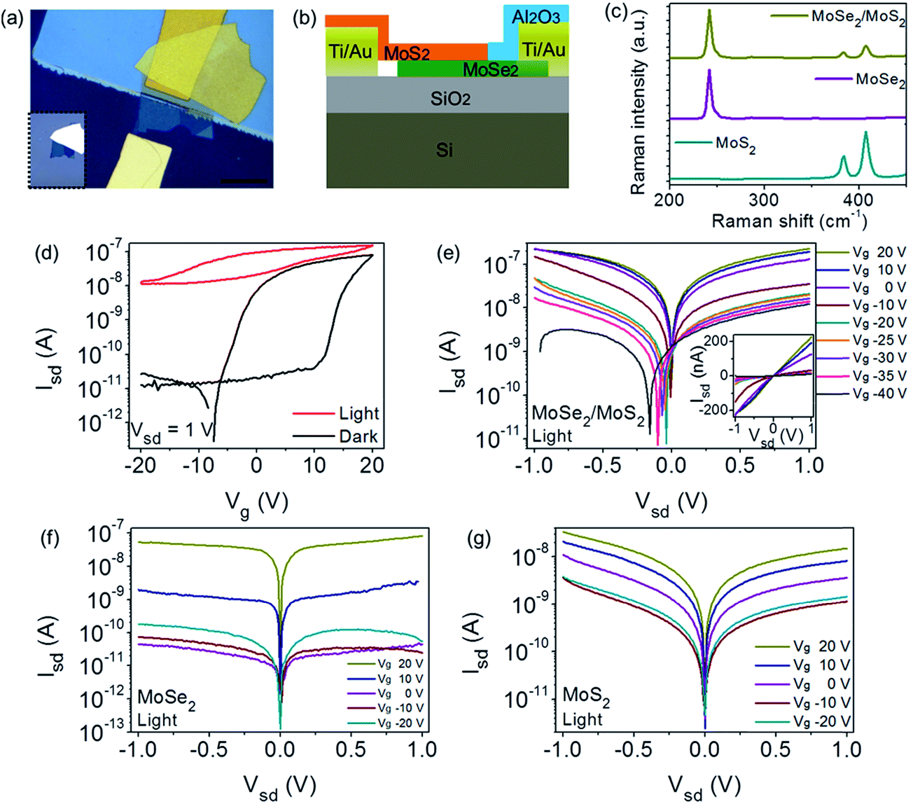 | ||
| Fig. 1 (a) Optical microscopy (OM) image of MoSe2/CVD–MoS2 heterojunctions based transistors with Ti (2 nm)/Au (50 nm) electrodes. The scale bar is 10 μm. The inset is the OM image of exfoliated MoSe2 before device fabrication. (b) Schematic of the heterojunction devices. (c) Raman spectra of MoSe2, MoS2 and the heterojunctions. (d) Transfer characteristics of the heterojunction devices under dark and light illumination at Vsd = 1 V. (e) Output characteristics (Isd–Vsd) of the devices for different back gate Vg under illumination with log scale of y-axis. The inset is the output curves in linear scale. (f, g) Output characteristics of pure MoSe2 and MoS2 transistors, respectively. | ||
To clearly investigate the gate modulated photovoltaic effect, we enlarged the I–V curves using light illumination and a different gate with linear and log scale of y-axis, respectively (Fig. 2a and b). Both Voc and short-circuit current (Isc) have been displayed in Fig. 2c, which evidently increased with increased negative back gate Vg. At negative back gate (Vg = −40 V), the Voc and Isc can reach up to 0.16 V and 1.3 nA, respectively. At positive gate (Vg > 0 V), the photovoltaic effect weakens with negligible Voc and Isc. We also measured the transfer curves with zero bias (Vsd = 0 V) and the time dependence of drain current as shown in Fig. 2d and the inset, respectively. The significant drain current at Vsd of 0 V indicates the formation of photocurrent, which also decreases with an increase in Vg. This is in good agreement with the results shown in Fig. 2c. Accordingly, the electrical power P can also vary with different gate voltage and reach the highest value at Vg of −40 V as shown in Fig. 2e. It is predicted that the electrical power has room for further improvement by the application of larger back gate. The fill factor (defined as FF = Pm/IscVoc) and the power conversion efficiency (defined as PCE = Pm/Pi = IscVocFF/Pi, where Pm is the maximum power and Pi is the given incident optical power) as a function of back gate are plotted in Fig. 2f. The FF is around 0.25 at negative gate region and the PCE can increase up to ∼0.5% with an increase in negative gate, which indicates the promising potential of our heterojunction device in solar cells application.
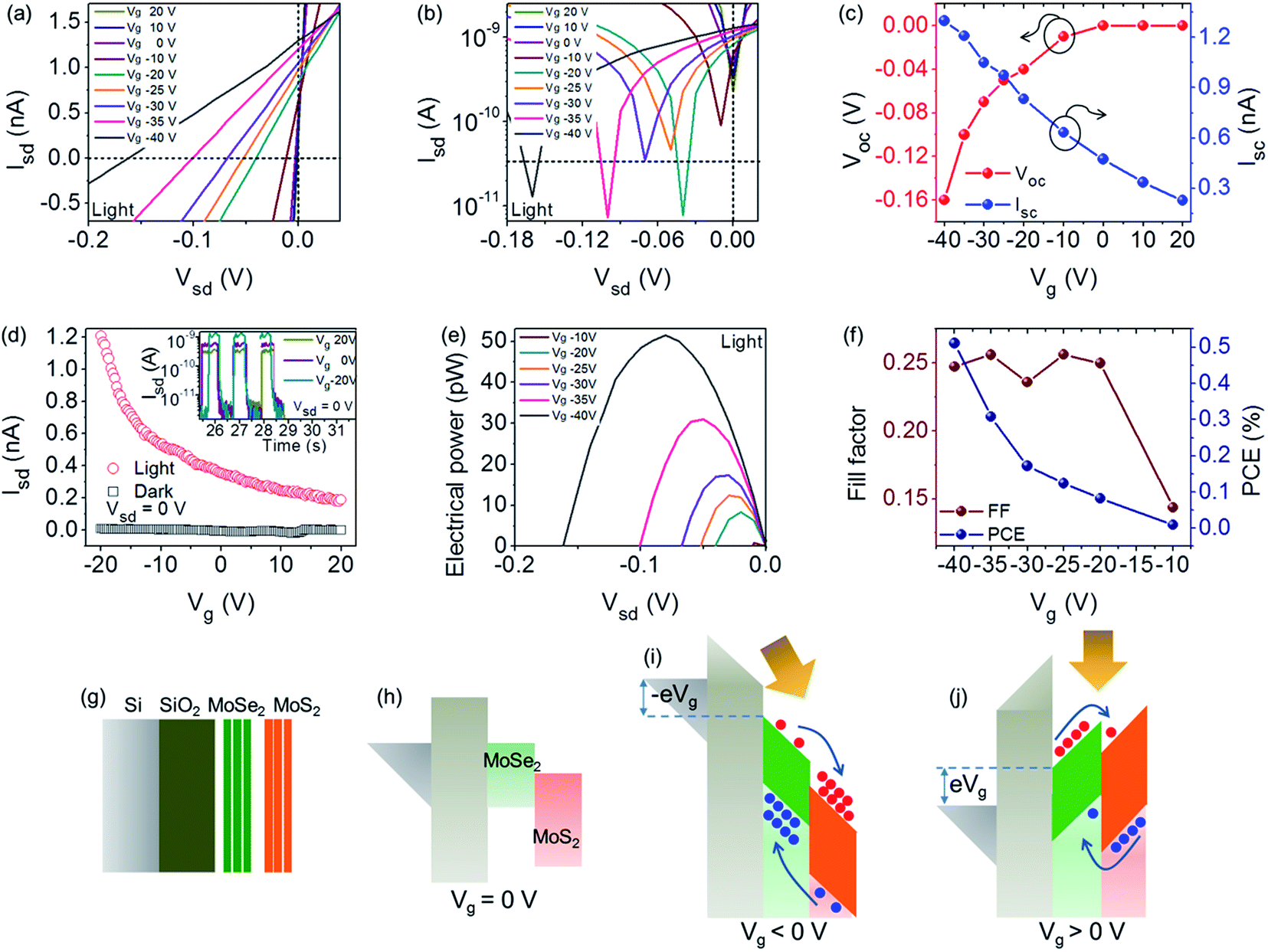 | ||
| Fig. 2 Enlarged output curves (Isd–Vsd) of the heterojuction devices with different back gate under light illumination in linear scale (a) and log scale of y-axis (b), showing the obvious photovoltaic effect. (c) Extracted open-circuit voltage Voc and short-circuit current Isc as a function of back-gate voltage Vg. (d) Transfer curves (Isd–Vg) of the heterojuction device at zero bias under dark and light illumination. The inset is time dependence of photocurrent at different back gate. (e) Electrical power P calculated at different gate voltage Vg. (f) Dependence of fill factor (FF) and power conversion efficiency (PCE) on back gate. (g) Schematic diagram of the heterojunction device. Energy band of the device with zero Vg (h), negative Vg (i) and positive Vg (j). | ||
To understand the gate modulated photovoltaic effect, the energy band diagram of the heterojunctions based devices has been plotted in Fig. 2g–j. Fig. 2g shows the schematic plot of the transistors in vertical architecture. Based on previous reports,14 MoSe2 can couple with MoS2 by type-II band alignment, as shown in Fig. 2h. The band shape of MoSe2/MoS2 and the effective barrier height at the interface can be effectively modulated by an external voltage Vg applied through the silicon back-gate electrode.8,10,15 With negative Vg, the MoSe2 and MoS2 are heavily hole-doped near the SiO2 substrate, resulting in a downward band slope across the entire stack from MoSe2 to MoS2 (Fig. 2i). In this case, the downward band slope can facilitate the transfer and separation of the photo-generated electrons and holes, leading to higher photocurrent and larger Voc and Isc. On the contrary, with positive Vg, the concentration of electrons in both MoSe2 and MoS2 increases near the SiO2 dielectric substrate and shifts the Fermi level upwards, forming an upward band slope (Fig. 2j). The upward band slope can result in an additional barrier for the carrier transfer at the interface, indicating that this substrate has a poor photovoltaic property. We now focus our attention to the photo-responsive property of the heterojunction transistors. Fig. 3a shows the temporal response of the transistors based on MoSe2/MoS2 heterojunctions and their components. Clearly, the photocurrent of the heterojunctions is improved by 1–2 orders of magnitude compared to that in isolated MoSe2 or MoS2. Moreover, the temporal response is ∼10 ms, which is equal to that in MoSe2 and much faster than that in MoS2. Moreover, the electrical response of the devices upon illumination is determined by their responsivity in units of A W−1, defined as R = Iph/PS where Iph is the photocurrent, P is the incident light power density and S is the active area. Fig. 3b shows the responsivity dependence on the optical intensity at Vsd of 1 V. The responsivity of the heterojunction transistors at Vg of 0 V is dramatically improved to ∼350 A W−1, which is about two orders of magnitude larger than that in the devices consisting of only MoSe2 (Fig. 3c) or MoS2 flakes (Fig. 3d). Moreover, the heterojunction device is more sensitive to illumination intensity as low as ∼0.1 μW cm−2. In all cases, the drop in responsivity with increasing incident optical power is due to the gradual saturation of the photo-sensitizing trap states under high light intensity in the heterojunctions flakes, which is in agreement with MoS2 based photodetectors.4
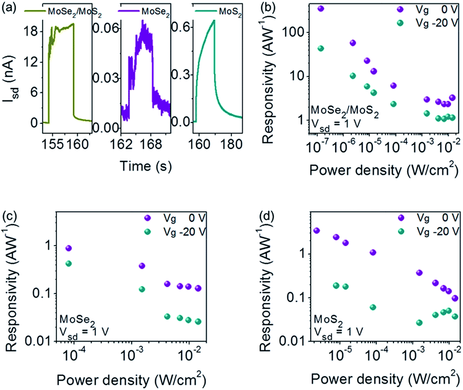 | ||
| Fig. 3 (a) Temporal response of the heterojunction, pure MoSe2 and MoS2 transistors at Vsd of 1 V and Vg of −20 V. The heterojuction device shows rapid decay time of ∼10 ms. (b) Dependence of the photo-responsivity on illumination intensity at different back gate and Vsd = 1 V for MoSe2/MoS2 heterojunction transistors. The device exhibits a higher responsivity of ∼350 A W−1 for low light power density at Vg = 0 V. (c, d) Photo-responsivity as a function of incident light power for MoSe2 and MoS2 only transistors, respectively. | ||
Conclusions
In summary, we have fabricated MoSe2 and CVD-grown MoS2 heterojunctions based transistors, which exhibit significant and gate modulated photovoltaic effect because of the gate tunable band slope. By forming the heterojunctions, the temporal response becomes rapid with a response time of ∼10 ms and a photo-responsivity of ∼350 A W−1, which has a dramatic improvement of around two orders of magnitude compared to the components MoSe2 or MoS2. Herein, we open up a new avenue of facile fabrication of 2D TMDs based transistors with promising potential applications in solar cells and photodetectors.Conflicts of interest
There are no conflicts of interest to declare.Acknowledgements
This study was supported by the “One-Hundred Talents Program” of Guangdong University of Technology (GDUT) and the National Natural Science Foundation of China under Grant No. 11674310.Notes and references
- B. Radisavljevic, M. B. Whitwickand and A. Kis, ACS Nano, 2011, 5, 9934–9938 CrossRef CAS PubMed
.
- L. Britnell, R. M. Ribeiro, A. Eckmann, R. Jalil, B. D. Belle, A. Mishchenko, Y.-J. Kim, R. V. Gorbachev, T. Georgiou, S. V. Morozov, A. N. Grigorenko, A. K. Geim, C. Casiraghi, A. H. Castro Neto and K. S. Novoselov, Science, 2013, 340, 1311–1314 CrossRef CAS PubMed
- M. M. Furchi, D. K. Polyushkin, A. Pospischil and T. Mueller, Nano Lett., 2014, 14, 6165–6170 CrossRef CAS PubMed
- O. Lopez-Sanchez, D. Lembke, M. Kayci, A. Radenovic and A. Kis, Nat. Nanotechnol., 2013, 8, 497–501 CrossRef CAS PubMed
- N. Huo, S. Yang, Z. Wei, S.-S. Li, J.-B. Xia and J. Li, Sci. Rep., 2014, 4, 5209 CrossRef CAS PubMed
- K. F. Mak and J. Shan, Nat. Photonics, 2016, 10, 216–226 CrossRef CAS
- C.-H. Lee, G.-H. Lee, A. M. van der Zande, W. Chen, Y. Li, M. Han, X. Cui, G. Arefe, C. Nuckolls, T. F. Heinz, J. Guo, J. Hone and P. Kim, Nat. Nanotechnol., 2014, 9, 676–681 CrossRef CAS PubMed
- N. Huo, J. Kang, Z. Wei, S.-S. Li, J. Li and S.-H. Wei, Adv. Funct. Mater., 2014, 24, 7025–7031 CrossRef CAS
- N. Huo, J. Yang, L. Huang, Z. Wei, S.-S. Li, S.-H. Wei and J. Li, Small, 2015, 11, 5430–5438 CrossRef CAS PubMed
- W. J. Yu, Z. Li, H. Zhou, Y. Chen, Y. Wang, Y. Huang and X. Duan, Nat. Mater., 2013, 12, 246 CrossRef CAS PubMed
- K. Roy, M. Padmanabhan, S. Goswami, T. P. Sai, G. Ramalingam, S. Raghavan and A. Ghosh, Nat. Nanotechnol., 2013, 8, 826 CrossRef CAS PubMed
- W. J. Yu, Y. Liu, H. Zhou, A. Yin, Z. Li, Y. Huang and X. Duan, Nat. Nanotechnol., 2013, 8, 952 CrossRef CAS PubMed
- R. Cheng, D. Li, H. Zhou, C. Wang, A. Yin, S. Jiang, Y. Liu, Y. Chen, Y. Huang and X. Duan, Nano Lett., 2014, 14, 5590–5597 CrossRef CAS PubMed
- J. Kang, S. Tongay, J. Zhou, J. Li and J. Wu, Appl. Phys. Lett., 2013, 102, 012111 CrossRef
- L. Britnell, R. V. Gorbachev, R. Jalil, B. D. Belle, F. Schedin, A. Mishchenko, T. Georgiou, M. I. Katsnelson, L. Eaves, S. V. Morozov, N. M. R. Peres, J. Leist, A. K. Geim, K. S. Novoselov and L. A. Ponomarenko, Science, 2012, 335, 947 CrossRef CAS PubMed
| This journal is © The Royal Society of Chemistry 2017 |