
 Open Access Article
 This Open Access Article is licensed under a Creative Commons Attribution-Non Commercial 3.0 Unported Licence
All-solution-processed fluorene/dibenzothiophene-S,S-dioxide blue co-oligomer light-emitting diodes with an electron transporting PEI/ultrafine-ZnO-nanoparticle bilayer†
Chun-Yuan Huang *a,
Chiao-Yang Chengb and
Yu-Shan Shiha
*a,
Chiao-Yang Chengb and
Yu-Shan Shiha
aDepartment of Applied Science, National Taitung University, Taitung 950, Taiwan. E-mail: laputa@nttu.edu.tw
bWafer Works Corporation, Longtan Science Park, Taoyuan 32542, Taiwan
First published on 29th August 2017
Abstract
In this article, an all solution-processed blue organic light-emitting diode (OLED) comprising the emissive fluorene/dibenzothiophene-S,S-dioxide co-oligomer, 3,7-bis[7-(9,9-di-n-hexylfluorenyl-2,7-diyl)-9,9-di-n-hexylfluoren-2-yl]-dibenzothiophene-S,S-dioxide (HFSO), and a poly-ethyleneimine (PEI)/ultrafine-ZnO-nanoparticle (NP) bilayer in the conventional device structure is proposed for the first time. The device configuration can be described as indium tin oxide (ITO)/poly(3,4-ethylenedioxythiophene):poly(styrenesulfonate) (PEDOT:PSS)/HFSO/PEI/ZnO-NP/Al. By carefully choosing the solvent for PEI, the PEI interlayer can be deposited without dissolving the underlying HFSO. Compared to our normal-sized ZnO NPs with the average size (ψavg) of 3.9 nm, the device with the ultrafine ZnO NPs (ψavg ∼ 2.9 nm) decreases the turn-on voltage from 3.3 to 2.9 V due to the reduction of the electron-encountered energy barrier. Furthermore, by inserting a PEI interlayer between the HFSO and ZnO layers, the device with an electron transporting bilayer can further improve the turn-on voltage and output luminance for the formation of a molecular dipole while avoiding the exciton quenching of HFSO from the adjacent ZnO. Thereby, the OLED with a PEI/ZnO-NP bilayer exhibits a blue electroluminescence peaked at 452 nm purely from HFSO, a very low turn-on voltage of ∼2.6 V, a high maximum luminance of ∼12![[thin space (1/6-em)]](https://www.rsc.org/images/entities/char_2009.gif) 000 cd m−2 at 7.6 V, a highest current efficiency of ∼1.55 cd A−1, and stable CIE coordinates of (0.144, 0.137).
000 cd m−2 at 7.6 V, a highest current efficiency of ∼1.55 cd A−1, and stable CIE coordinates of (0.144, 0.137).
I. Introduction
Since the first demonstration of efficient organic light-emitting diodes (OLEDs) by Tang and VanSlyke in 1987,1 OLED technology has evolved rapidly with the result that numerous OLED-based display panels and even solid state lighting systems are now commercially available.2 Despite the success and outstanding performance of OLED devices, penetrating wider markets is still a significant challenge due to the high manufacturing costs involved.3 For example, current commercialized OLEDs generally consist of small molecules deposited in an expensive and time-consuming vacuum evaporation process. Sophisticated device encapsulation is also required to protect the oxygen/water-vulnerable organic materials, which also makes the reduction in production costs very difficult.4Small molecules are easy to synthesize and purify. Their vacuum deposition ensures that complicated device structures with multiple organic layers can be easily realized. However, the equipment required for vacuum deposition is expensive. In an actual evaporation process, only ∼20% of the costly OLED-materials are used.5 Alternatively, because the polymer light-emitting diodes (PLEDs) feature their simple and variable wet process, it is a brilliant strategy to fit the small-molecule OLEDs with these well-developed fabrication procedures such as spin-coating, inkjet printing, and roll-to-roll imprinting.
On the other hand, one of the simplest approaches for fabricating air-stable EL devices is to substitute organic materials with inorganic ones, such as transparent metal oxides and semiconductor quantum dots (QDs).6 Vasilopoulou et al. fabricated an unencapsulated OLED with an inorganic WO2.5 hole injection layer, and showed that the device had a lifetime of more than 700 hours in ambient air.6a Hybrid LEDs with inorganic CdSe/ZnS or CdSe/CdS QD emitters (so-called quantum dot light-emitting diodes (QDLEDs or QLEDs)) have attracted world-wide attention as a promising technology for the realization of high color purity, high stability displays.6e,f For those reported OLEDs or QLEDs with electron transporting sol-gel-derived metal oxide layers, the inverted device structure with indium tin oxide (ITO)-cathode was typically adopted to avoid the damage of organic materials by the essential high-temperature annealing of metal oxides.6a–d In a conventional device configuration with ITO-anode, the present study proposes an all-solution-processed blue OLED which comprises the fluorescent co-oligomer, 3,7-bis[7-(9,9-di-n-hexylfluorenyl-2,7-diyl)-9,9-di-n-hexylfluoren-2-yl]-dibenzothiophene-S,S-dioxide (HFSO), and an electron transporting bilayer consisting of poly-ethyleneimine (PEI) and ultrafine ZnO nanoparticles (NPs). The electron deficient unit, dibenzothiophene-S,S-dioxide, in the HFSO was recently demonstrated to be incorporated into polyfluorenes for efficient electroluminescent devices.7 PEI is air-stable and frequently used in organic electronic or optoelectronic devices to modify the work function of adjacent layer for better energy band alignment.8a Also, the electron-rich nitrogen atoms in PEI can trap holes to achieve hole-blocking.8b The band-gap energy (Eg) of ZnO bulk at room temperature is 3.37 eV.9 By reducing the volume of ZnO to be ultrafine nanoparticles (ψavg ∼ 2.9 nm), Eg can be increased to 3.65 eV for better energy-level alignment. Notably, the PEI interlayer can be spin-coated on the HFSO emission layer (EML) without any damage or intermixing, and is resistive to the following dynamic spin-coating of ZnO-NP layer. The fabricated simple device, as a result, has good spectral stability with a low turn-on voltage (∼2.6 V), a high maximum luminance (∼12000 cd m−2 at 7.6 V) and a moderate current efficiency (∼1.55 cd A−1).
II. Results and discussion
Preparation of HFSO blue emitter and ZnO NPs
Our HFSO blue emitter was dissolved in toluene with a concentration of 1.2 wt%. As mentioned in previous studies,10 the strong blue fluorescence of the HFSO molecules results from the incorporation of dibenzothiophene-S,S-dioxide (SO) units into the oligofluorenes (see Fig. 1(a)). SO is also a good electron withdrawing unit. By incorporating it into oligomers or polymers, the electron transportation capability and thermal stability can be improved.10 In this study, the absolute quantum yield of HFSO was measured to be 82.5%. As shown in Fig. 1(b), the first absorption and photoluminescence (PL) peaks of the HFSO solution are located at 379 and 433 nm, respectively. The HFSO was recently demonstrated to be a good matrix to hybridize with orange-emitting CsPbBr1.5I1.5 perovskite QDs for white electroluminescence.11 Our ZnO NPs were synthesized at room temperature using the sol–gel method previously reported by the present group.12 However, to achieve a smaller particle size and a more uniform size-distribution, the growth time was reduced and the sol stabilizer was added before NP nucleation for chelation control. The purified ultrafine ZnO NPs were dispersed in ethanol with a concentration of 25 mg mL−1 for device fabrication. Comparing to the ZnO NPs with the normal size of ∼3.9 nm (NSNPs) which exhibited the absorption peak at 336 nm,12 the resulting solution of ultrafine NPs (UFNPs) exhibited a strong and more distinct absorption peak at 319 nm (see Fig. 1(b)), indicating a more uniform size-distribution and a more dramatic quantum-confinement effect due to the smaller particle size. Thereby, the UFNP size was estimated to be ∼2.9 nm, while Eg was obtained empirically as 3.65 eV.13 Similar to the absorption spectrum, the PL peak is also blue-shifted (530 to 507 nm) after reducing the size. From the previous study, the size-dependent visible PL of ZnO NPs can be attributed to the variation of energy difference between the valence band edge and the deep donor energy level related to the ionized oxygen vacancies.14 Therefore, the strong visible PL indicates that there are plenty of oxygen vacancies existing in the particle surface. In Fig. 1(c), both of the HFSO and UFNP solutions look highly-transparent. Under UV irradiation, bright blue emission and broad light-cyan emission band are observed from the HFSO and UFNP solutions, respectively. Our ZnO NP solutions can be stored at room temperature for over three months without turbidity or precipitation. However, the absorption peak is red-shifted with storage time. As shown in Fig. 2, the peak of UFNP shifts to 335 nm, while that of the NSNP shifts from 336 to 340 nm after storage for 1400 hours. Actually, we can synthesize the blue-emitting ZnO NP solution by reducing the synthesis temperature, but it was unstable and rapidly changed to be cyan-emitting within one day implying the quick growth of nanoparticles (Fig. S1, see ESI†). To prevent the uncertainty of NPs' unintentional growth, the blue-emitting ZnO NPs was not used in the following discussion and all the characterization and device fabrication were carried out within one day after the NPs were prepared. Fig. S2† shows the X-ray diffraction (XRD) patterns of the NSNPs and UFNPs, respectively. The crystalline orientation of the wurtzite ZnO is not affected by adding the stabilizer during particle's nucleation, except the weaker peak intensities and more pronounced peak broadening for the UFNPs. The electron mobilities of ZnO NPs were evaluated using an electron-only device consisting of a ZnO-NP layer sandwiched between two Al electrodes.15 As shown in Fig. 3, the current density–voltage (J–V) curve of the device is well-fitted by the power law J–Vn, where n ∼ 1 represents the ohmic region and n ∼ 2 is the space-charge-limited-current (SCLC) region. Applying Child's law to the fitted results in the SCLC region, the electron mobilities are about 5.2 × 10⁻⁴ and 1.5 × 10⁻³ cm2 V−1 s−1 for the UFNPs and NSNPs, respectively.16 Table 1 shows the comparison of electron mobility of ZnO NPs with different average sizes based on theory of SCLC or thin-film transistor (TFT). The values for our NSNPs and UFNPs are slightly smaller than those reported ones,16 probably due to the difference of preparation method and the influence of post-deposition treatment. A high resolution transmission electron microscopy (TEM) image of a UFNP is shown in the inset of Fig. 3, the lattice fringes are clearly observed.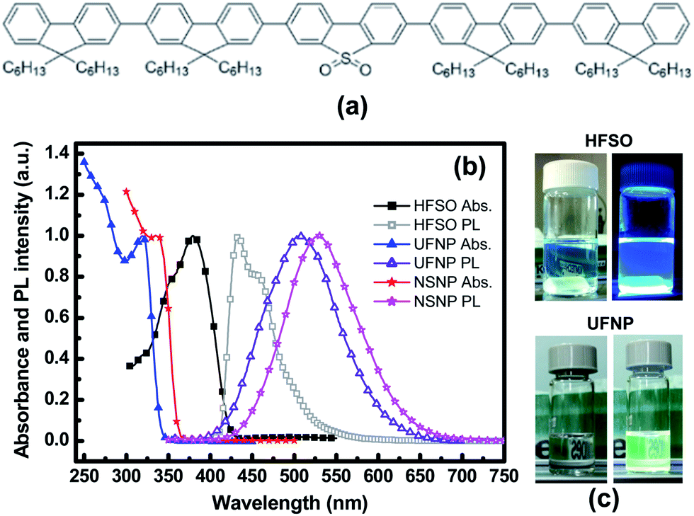 | ||
| Fig. 1 (a) Chemical structure of HFSO, (b) normalized absorption and PL spectra of HFSO, NSNP, and UFNP solutions, and (c) photographs of HFSO and UFNP solutions with and without UV irradiation. | ||
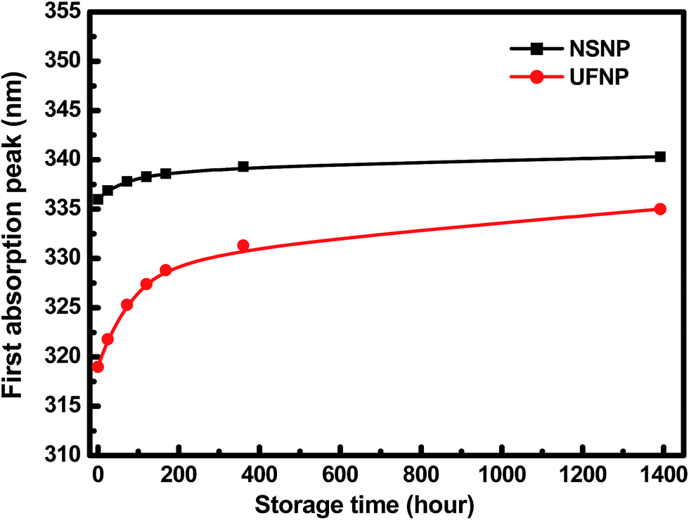 | ||
| Fig. 2 Time-dependent first absorption peak position of NSNP and UFNP solutions. The red-shift of peak position with time indicates the growth of ZnO NPs, even though they were twice purified before being redispersed in ethanol. | ||
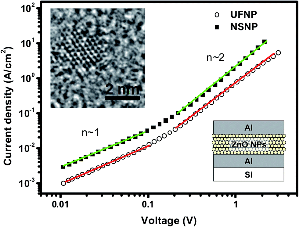 | ||
| Fig. 3 Current density–voltage (J–V) curves of electron-only device. Insets show a schematic representation of the device structure and a TEM image of a UFNP with size ∼2.6 nm. | ||
Fabrication of blue-emitting co-oligomer light-emitting diodes
Fig. 4(a) presents a schematic illustration of the complete OLED structure. In fabricating the device, a patterned ITO glass substrate was ultrasonically cleaned in acetone, isopropyl alcohol and di-ionized water, and was then UV-ozone treated for 25 minutes. A thin poly(3,4-ethylenedioxythiophene):poly(styrenesulfonate) (PEDOT:PSS) hole injection layer (through a 0.45 μm syringe filter) and an HFSO EML were then spin-coated at 4000 and 3000 rpm and baked at 150 and 100 °C for 30 minutes, respectively. Prior to the coating of ZnO-NP layer, a thin PEI interlayer was spin-coated on the HFSO from the PEI/ethanol solution (0.3 wt%). It should be mentioned that the PEI was used instead of polyethyleneimine ethoxylated (PEIE) or Cs2CO3 because of its higher [N+]/[C] ratio to lower the energy barrier as previously demonstrated.17 A close-packed layer of UFNPs was then coated onto the PEI interlayer and baked at 70 °C for 30 minutes to finish the electron transporting bilayer. Finally, a 120 nm-thick Al layer was thermally evaporated at 5 × 10⁻⁶ torr to complete the device. Two reference devices with the UFNP and NSNP layers respectively deposited on the HFSO without the PEI interlayer were fabricated for comparison. For convenience in the following discussion, the devices with the NSNP, UFNP, and PEI/UFNP layers are referred to hereafter simply as the NSNP-, UFNP-, and PEINP-devices, respectively.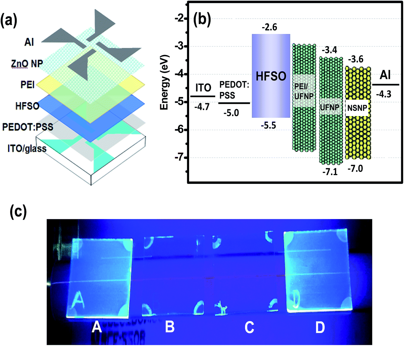 | ||
| Fig. 4 (a) Schematic device structure and (b) corresponding energy band model of complete NSNP-, UFNP-, and PEINP-devices. (c) Photographs of UV-irradiated HFSO films before and after washing in various solvents (A: pristine HFSO film; B: washing in hexane; C: washing in chlorobenzene; D: washing in ethanol). The valence band edge levels of NSNP, UFNP, and HFSO layers are determined by ultraviolet photoelectron spectroscopy (UPS) analysis shown in Fig. S3 and S4.† | ||
In the proposed schematic energy band diagram shown in Fig. 4(b), the ZnO layer facilitates electron injection while also keeping the hole within the EML; thereby increasing the probability of radiative recombination. The increase of effective Eg of ZnO NPs by reducing the size clearly turns to the reduction of mismatch of conduction band edges of HFSO and ZnO NPs. A key concern to successfully fabricate our all-solution-processed devices is to prevent the intermixing of HFSO, PEI, and ZnO NPs with one another possibly caused by successive spin coating. Before the implementation of device fabrication, therefore, different solvents were spun on the HFSO layer in order to evaluate its solvent resistance. The photograph presented in Fig. 4(c) show that the HFSO film is less affected by ethanol than by hexane or chlorobenzene. Thus, PEI or ZnO NPs dissolved in ethanol is suitable for deposition on the EML. However, the dissolution of PEI in ethanol is not straightforward. PEI is practically resistant to ethanol and can be merely dissolved at low concentration with continuous stirring at 60 °C for 24 hours. Even though, to prevent the dissolution of PEI interlayer by ethanol, the UFNPs were deposited onto the PEI using an “on-the-fly-dispensing spin coating” method, with which the UFNP-solution was dispensed on a highly rotated substrate. The atomic force microscopy (AFM) images presented in Fig. 5 show the variation of surface morphology of layers in sequence of deposition. With a thickness of 140 nm and a very low sheet resistance of ∼7 ohm □−1, the ITO crystal grains coalesce with one another to be larger crystal domains which result in a poor film morphology and a very high root-mean-square roughness (Ra) of 5.2 nm. The deposition of PEDOT:PSS not only facilitates the hole injection but also flattens the surface (Ra ∼ 2.4 nm) for uniform current injection. Furthermore, the surfaces of the HFSO EML and PEI/UFNP bilayer are very smooth and contain no voids, clusters or particle-aggregation, no matter whether the PEI interlayer is inserted or not.
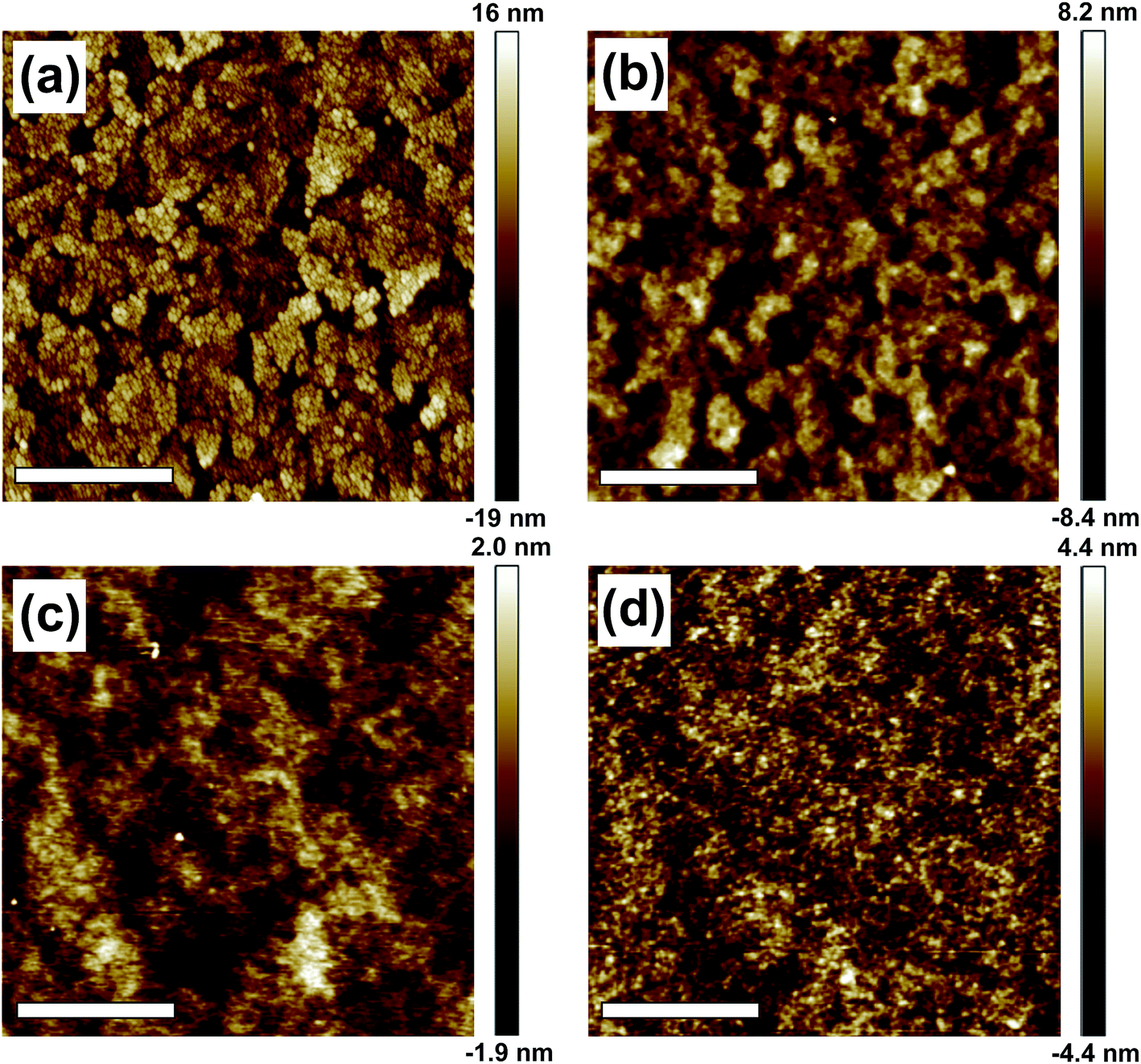 | ||
| Fig. 5 AFM images of (a) ITO, (b) PEDOT:PSS, (c) HFSO, and (d) UFNP layers. The Ra of each layer is 5.2, 2.4, 0.6, and 1.3 nm, respectively. The scale bars are 1 μm. | ||
The luminance–current density–voltage (L–J–V) curves of the three devices are shown in Fig. 6(a). The NSNP-, UFNP- and PEINP-devices have turn-on voltages (Vt) of 3.3, 2.9 and 2.6 V, while the maximum luminance (Lmax) at 7.6 V is 2700, 7300, and 12000 cd m−2, respectively. Based on previous studies,13,18 when the size of the ZnO NP is reduced to smaller than 7 nm, the quantum confinement effect makes the effective Eg rapidly increase. As aforementioned, for the particle size of 3.9 and 2.9 nm, Eg of the ZnO NP is about 3.43 and 3.65 eV, respectively. From the energy band diagram shown in Fig. 4(b), we can basically infer that the hole is the dominant carrier in the EML because the HFSO is a hole transporter (p-type) and the hole can inject at lower voltages in all devices. Despite the slightly higher leakage current, it can be estimated that the hole injection occurs at voltages between 1.0 and 3.0 V in the NSNP-device. And apparently, the onset of the electron injection is at ∼3.3 V because of the observation of light emission. By contrast, in the UFNP-device, the electron injects into the EML at ∼3.0 V, which is close to the voltage for the hole injection and achieves a better charge balance in HFSO for efficient radiative recombination.19 The reduction of Vt (∼0.3 V) is higher than the energy discrepancy (∼0.2 eV) of conduction band edges of UFNPs and NSNPs, probably with the enhancement of Auger-assisted energy up-conversion process suggested by Qian et al.20 Also, by reducing the leakage current observed in the NSNP-device, the UFNP-device can achieve higher Lmax (7300 cd m−2) and similar current efficiency (ηc) (1.13 cd A−1, see Fig. 6(b)) compared to those (4300 cd m−2 and 1.12 cd A−1) of the counterpart with Ca/Al cathodes in our previous study.12 Since the recombination zone of excitons is close to the interface of HFSO and ZnO NP, the improvement of Lmax can be attributed to the elimination of exciton quenching caused by Ca2+ diffusion.21
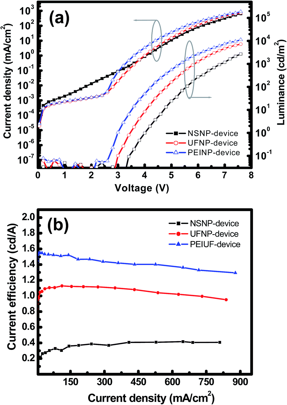 | ||
| Fig. 6 (a) L–J–V and (b) ηc–J characteristics of NSNP-, UFNP- and PEINP-devices. | ||
With the further insertion of PEI interlayer in the PEINP-device, Vt is correspondingly reduced to 2.6 V. Typically, the onset of light emission is determined by the minority carrier, which is the electron in our case. In this stage, the improvement in Vt should be attributed to the enhancement of the electron injection induced by the presence of dipoles at the interface, as well as the reduction of the exciton dissociation in EML induced by directly contacting ZnO.17a Regarding the very high luminance and efficiency achieved by phosphorescent or thermally activated delayed fluorescence (TADF) lumophores with complicated device architectures,21 it is noticeable that however, the Lmax (12000 cd m−2) of the PEINP-device is larger than that of the reported fluorescent OLEDs with blue fluorophores or polymers grafting with similar SO derivatives, and an ultrathin layer of alkali metal fluorides which is supposed to entirely eliminate the electron injection barrier.22 In Fig. 6(b), the UFNP- and PEINP-devices also exhibit high operating stability, in other words, very low efficiency roll-off. When the current density increases to ∼750 mA cm−2, ηc of the UFNP- and PEINP-devices decreases only 13% and 15% of its maximum values, respectively.
Fig. 7 shows the normalized EL spectra of the PEINP-device at different current densities, to which the spectra of the NSNP- and UFNP-devices are very similar and not shown. The main peak in the EL spectrum of the PEINP-device is located at ∼452 nm accompanying a shoulder peak (at ∼468 nm) with a comparable intensity. The EL spectra are identical to the PL spectra of HFSO film, but they are ∼19 nm red-shifted compared to that of HFSO solution. For fluorescent oligomers or polymers, this red-shift accompanying peak broadening is typically attributed to the intermolecular interaction due to the aggregation in the solid state.23 It is also seen that, the EL spectra are almost unchanged at different applied current density ranging from 35 to 700 mA cm−2, showing high spectral stability. In previous studies, the SO units in a polyfluorene-derivative were inferred to act as deep electron traps to promote efficient blue EL emission.24 The SO units can also increase the glass transition and decomposition temperatures to improve the copolymers' thermal and spectral stabilities.10b In addition, no defective emission from ZnO NPs was observed in our devices because of the deep valence band edge of NSNPs and UFNPs for efficient hole blocking. The high spectral stability makes the constant CIE-1931 chromaticity coordinates of (0.144, 0.137) in whole operation range. The insets of Fig. 7 show the EL emissions of the PEINP-device biased at 35 and 700 mA cm−2, respectively. It is clearly observed that the emission intensity is very uniform at low current density, without significant damage induced by PEI or UFNP coating. Based on our demonstration, the performance of OLEDs with conventional fluorescent oligomers and low work function metals can be further improved by providing better matches of adjacent energy levels via the PEI/UFNP bilayer. To increase the efficiency of blue OLEDs with ultrafine ZnO NPs, we are currently investigating the solution-processable phosphorescent materials to replace HFSO, and the results will be published elsewhere.
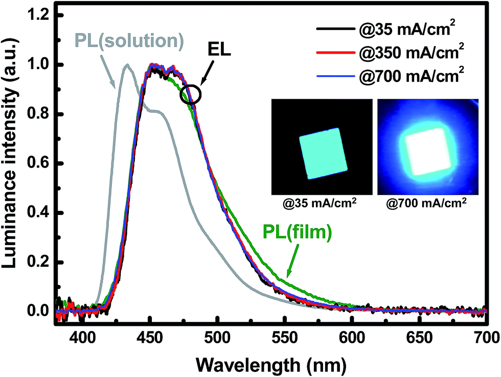 | ||
| Fig. 7 Normalized EL spectra of PEINP-device at different current densities and PL spectra of HFSO solution and film. Note that the insets show the EL emissions of the PEINP-device biased at 35 and 700 mA cm−2, respectively. | ||
III. Conclusion
In conclusion, a solution-processed blue OLED comprising the fluorene/dibenzothiophene-S,S-dioxide co-oligomer, HFSO, and a hybrid PEI/UFNP bilayer has been presented. Compared to the normal-sized ZnO NPs (ψavg ∼ 3.9 nm) synthesized via widely used sol–gel route, the ultrafine ZnO NPs with ψavg of ∼2.9 nm can be achieved by controlling the growth time and stabilizer. By fabricating the electron-only device with configuration of Al/ZnO-NPs/Al, the electron mobility was calculated as 5.2 × 10⁻⁴ and 1.5 × 10⁻³ cm2 V−1 s−1 for the UFNPs and NSNPs, respectively. The UFNPs can be readily deposited on the PEI interlayer without destroying the underlying HFSO layer, and result in a spectrally-stable device with a low turn-on voltage of ∼2.6 V, a high maximum luminance of ∼12000 cd m−2 at 7.6 V, a current efficiency of ∼1.55 cd A−1, and stable CIE coordinates of (0.144, 0.137).
IV. Experimental section
Chemical
Zinc acetate dihydrate (Zn(CH3COO)2·2H2O, >98%, Aldrich), tetramethylammonium hydroxide (TMAH, 25% in methanol, Alpha Aesar), monoethanolamine (MEA, 97%, Aldrich), poly-ethyleneimine (PEI, Mw ∼ 25000, Aldrich), dimethyl sulfoxide (DMSO, 99.5%, Panreac), ethyl acetate (99.5%, Panreac), ethanol (99.5%, Panreac), toluene (99%, Aldrich), PEDOT:PSS (Baytron AI 4083, HC Starck) were used in an as-received condition without further purification.
Synthesis of ultrafine ZnO NPs
In a typical synthesis, a 15 mL solution of 0.1 M zinc acetate dihydrate and MEA dissolved in DMSO was stirred at room temperature for 30 minutes. 5 mL of a 0.55 M solution of TMAH in ethanol was then dropwisely added within 10 minutes and the reaction solution was allowed to stand at room temperature for one hour. The ultrafine ZnO NPs were precipitated by adding ethyl acetate and redispersed in ethanol.Characterization
The phases of ZnO NPs were characterized by grazing incidence X-ray diffraction (GIXRD) using a Rigaku RINT2000 diffractometer with Cu Kα radiation. UV-vis absorption and PL spectra were obtained using a UV-vis spectrophotometer (HP 8453, Agilent) and a fluorescence spectrophotometer (Fluoromax-4, Horiba Jobin Yvon), respectively. AFM images and UPS spectra were obtained using an atomic force microscope (Model Innova, Bruker) and an electron spectrometer (ULVAC-PHI, Chigasaki), respectively. Absolute QY of HFSO solution was measured by the fluorescence spectrophotometer (Fluoromax-4, Horiba Jobin Yvon) combined with an integrating sphere (Quanta-φ) for collecting the emission light. Current–voltage characteristics of the OLEDs were measured using a Keithley 2400 source meter. Moreover, the luminance properties under various voltages were obtained by calibrating the photocurrent of a silicon detector using a luminance meter (LS-110, Minolta).Conflicts of interest
There are no conflicts to declare.Acknowledgements
The authors would like to thank the Ministry of Science and Technology of Taiwan, R.O.C. for the financial support of this study under Contract No. MOST 104-2221-E-143-003-MY2 and 106-2221-E-143-006.References
- C. W. Tang and S. A. VanSlyke, Appl. Phys. Lett., 1987, 51, 913 CrossRef CAS.
- (a) K. Kato, T. Iwasaki and T. Tsujimura, J. Photopolym. Sci. Technol., 2015, 28, 335 CrossRef CAS; (b) http://www.samsung.com/global/microsite/oledtv.
- (a) H. J. Shin, S. Takasugi, K. M. Park, S. H. Choi, Y. S. Jeong, B. C. Song, H. S. Kim, C. H. Oh and B. C. Ahn, Proc. Soc. Inform. Display Symp. Dig. Tech. Papers, 2015, 46, 53 CrossRef CAS; (b) R. Q. Ma, R. Hewitt, K. Rajan, J. Silvernail, K. Urbanik, M. Hack and J. J. Brown, J. Soc. Inf. Disp., 2008, 16, 169 CrossRef.
- S. Seo, H. Chae, S. Seo, H. K. Chung and S. Cho, Appl. Phys. Lett., 2013, 102, 161908 CrossRef.
- L. Duan, L. Hou, T. Lee, J. Qiao, D. Zhang, G. Dong, L. Wang and Y. Qiu, J. Mater. Chem., 2010, 20, 6392 RSC.
- (a) M. Vasilopoulou, G. Apadimitropoulos, L. C. Palilis, D. G. Georgiadou, P. Argitis, S. Kennou and D. Davazoglou, Org. Electron., 2012, 13, 796 CrossRef CAS; (b) C. Y. Huang, C. C. Yang, H. C. Yu and Y. C. Chen, J. Appl. Phys., 2014, 115, 083109 CrossRef; (c) S. H. Liao, H. J. Jhuo, P. N. Yeh, Y. S. Cheng, Y. L. Li, Y. H. Lee, S. Sharma and S. A. Chen, Sci. Rep., 2014, 4, 6813 CrossRef CAS PubMed; (d) C. Y. Huang and Y. C. Chen, Int. J. Electrochem. Sci., 2013, 8, 3572 CAS; (e) C. J. Chen, R. K. Chiang, C. Y. Huang, J. Y. Lien and S. L. Wang, RSC Adv., 2015, 5, 9819 RSC; (f) H. T. Vu, R. K. Chiang, C. Y. Huang, C. J. Chen, H. C. Yu, J. Y. Lien and Y. K. Su, Appl. Phys. Express, 2016, 9, 082101 CrossRef.
- (a) J. Liang, L. Ying, W. Yang, J. Peng and Y. Cao, J. Mater. Chem. C, 2017, 5, 5096 RSC; (b) F. Peng, T. Guo, L. Ying, W. Yang, J. Peng and Y. Cao, Org. Electron., 2017, 48, 118 CrossRef CAS.
- (a) Y. Zhou, C. Fuentes-Hernandez, J. Shim, J. Meyer, A. J. Giordano, H. Li, P. Winget, T. Papadopoulos, H. Cheun, J. Kim, M. Fenoll, A. Dindar, W. Haske, E. Najafabadi, T. M. Khan, H. Sojoudi, S. Barlow, S. Graham, J. Brédas, S. R. Marder, A. Kahn and B. Kippelen, Science, 2012, 336, 327 CrossRef CAS PubMed; (b) B. Sun, W. Hong, E. Thibau, H. Aziz, Z. Lu and Y. Li, ACS Appl. Mater. Interfaces, 2015, 7, 18662 CrossRef CAS PubMed.
- D. W. Hamby, D. A. Lucca, M. J. Klopfstein and G. Cantwel, J. Appl. Phys., 2003, 93, 3214 CrossRef CAS.
- (a) I. I. Perepichka, I. F. Perepichka, M. R. Bryce and L. Palsson, Chem. Commun., 2005, 27, 3397 RSC; (b) R. He, J. Xu, Y. Xue, D. Chen, L. Ying, W. Yang and Y. Cao, J. Mater. Chem. C, 2014, 2, 7881 RSC.
- C. Y. Huang, S. J. Huang and M. H. M. Liu, Org. Electron., 2017, 44, 6 CrossRef CAS.
- C. Y. Huang and J. H. Lai, Org. Electron., 2016, 32, 244 CrossRef CAS.
- E. A. Meulenkamp, J. Phys. Chem. B, 1998, 102, 5566 CrossRef CAS.
- (a) L. Zhang, L. Yin, C. Wang, N. Lun, Y. Qi and D. Xiang, J. Phys. Chem. C, 2010, 114, 9651 CrossRef CAS; (b) H. M. Xiong, D. G. Shchukin, M. Helmuth, X. Yang and Y. Y. Xia, Angew. Chem., Int. Ed., 2009, 48, 2727 CrossRef CAS PubMed.
- X. Dai, Z. Zhang, Y. Jin, Y. Niu, H. Cao, X. Liang, L. Chen, J. Wang and X. Peng, Nature, 2014, 525, 96 CrossRef PubMed.
- (a) J. Pan, J. Chen, Q. Huang, Q. Khan, X. Liu, Z. Tao, Z. Zhang, W. Lei and A. Nathan, ACS Photonics, 2016, 3, 215 CrossRef CAS; (b) J. Kwak, W. Bae, D. Lee, I. Park, J. Lim, M. Park, H. Cho, H. Woo, D. Y. Yoon, K. Char, S. Lee and C. Lee, Nano Lett., 2012, 12, 2362 CrossRef CAS PubMed; (c) L. Qian, Y. Zheng, J. Xue and P. H. Holloway, Nat. Photonics, 2011, 5, 543 CrossRef CAS; (d) A. L. Roest, J. J. Kelly, D. Vanmaekelbergh and E. A. Meulenkamp, Phys. Rev. Lett., 2002, 89, 036801 CrossRef CAS PubMed; (e) C. Jiang, H. Liu, B. Liu, Z. Zhong, J. Zou, J. Wang, L. Wang, J. Peng and Y. Cao, Org. Electron., 2016, 31, 82 CrossRef CAS.
- (a) Y. Kim, T. Han, H. Cho, S. Min, C. Lee and T. Lee, Adv. Funct. Mater., 2014, 24, 3808 CrossRef CAS; (b) C. Y. Huang and Y. C. Chen, Int. J. Electrochem. Sci., 2013, 8, 3572 CAS.
- K. F. Lin, H. M. Cheng, H. C. Hsu, L. J. Lin and W. F. Hsieh, Chem. Phys. Lett., 2005, 409, 208 CrossRef CAS.
- S. Y. Yu, D. C. Huang, Y. L. Chen, K. Y. Wu and Y. T. Tao, Langmuir, 2012, 28, 424–430 CrossRef CAS PubMed.
- L. Qian, Y. Zheng, K. R. Choudhury, D. Bera, F. So, J. Xue and P. H. Holloway, Nano Today, 2010, 5, 384 CrossRef CAS.
- (a) S. Purandare, E. F. Gomez and A. J. Steckl, Nanotechnology, 2014, 25, 094012 CrossRef PubMed; (b) Z. Yang, Z. Mao, Z. Xie, Y. Zhang, S. Liu, J. Zhao, J. Xu, Z. Chi and M. P. Aldred, Chem. Soc. Rev., 2017, 46, 915 RSC.
- (a) T. Guo, L. Yu, B. Zhao, L. Ying, H. Wu, W. Yang and Y. Cao, Polym. Chem., 2015, 53, 1043 CrossRef CAS; (b) J. Xu, Y. Yang, B. Zhang, W. Yang and Y. Cao, Dyes Pigm., 2017, 138, 245 CrossRef CAS; (c) J. H. Cook, J. Santos, H. Li, H. A. Al-Attar, M. R. Bryce and A. P. Monkman, J. Mater. Chem. C, 2014, 2, 5587 RSC.
- L. Wang, W. Y. Wong, M. F. Lin, W. K. Wong, K. W. Cheah, H. L. Tam and C. H. Chen, J. Mater. Chem., 2008, 18, 4529 RSC.
- (a) Y. Li, H. Wu, J. Zou, L. Ying, W. Yang and Y. Cao, Enhancement of spectral stability and efficiency on blue light-emitters via introducing dibenzothiophene-S, S-dioxide isomers into polyfluorene backbone, Org. Electron., 2009, 10, 901–909 CrossRef CAS; (b) K. C. Moss, K. N. Bourdakos, V. Bhalla, K. T. Kamtekar, M. R. Bryce and A. P. Monkman, Tuning the intramolecular charge transfer emission from deep blue to green in ambipolar systems based on dibenzothiophene S,S-dioxide by manipulation of conjugation and strength of the electron donor units, J. Org. Chem., 2010, 75, 6771–6781 CrossRef CAS PubMed.
Footnote |
| † Electronic supplementary information (ESI) available. See DOI: 10.1039/c7ra07652e |
| This journal is © The Royal Society of Chemistry 2017 |