
 Open Access Article
 This Open Access Article is licensed under a
 Creative Commons Attribution 3.0 Unported Licence
Facile one-pot synthesis of 3D graphite–SiO2 composite foam for negative resistance devices†
Ye Wu a,
Hao Fub,
Amitava Royc,
Pengfei Songb,
Yingcheng Lin*de,
Orhan Kizilkaya*c and
Jian Xu*a
a,
Hao Fub,
Amitava Royc,
Pengfei Songb,
Yingcheng Lin*de,
Orhan Kizilkaya*c and
Jian Xu*a
aDivision of Electrical and Computer Engineering, College of Engineering, Louisiana State University, Baton Rouge, LA 70803, USA. E-mail: jianxu1@lsu.edu
bDepartment of Mechanical Engineering, McGill University, 817 Sherbrooke St. West, Room 270, Montreal, Quebec H3A 0C3, Canada
cCenter for Advanced Microstructures & Devices, Louisiana State University, 6980 Jefferson Highway, Baton Rouge, LA 70806, USA. E-mail: orhan@lsu.edu
dKey Laboratory of Dependable Service Computing in Cyber Physical Society (Chongqing University) of Ministry of Education, Chongqing 400044, China. E-mail: linyc@cqu.edu.cn
eCollege of Communication Engineering, Chongqing University, Chongqing 400044, China
First published on 29th August 2017
Abstract
In this study, we successfully prepare a porous graphite–SiO2 composite foam via a facile glucose-foaming-based method. The foam was characterized by XRD, XPS, SEM, Raman, and soft X-ray absorption spectroscopy of the carbon and oxygen K-edges and by silicon K-edge X-ray absorption near edge structure (XANES) spectroscopy. The electrical properties of the sample were evaluated using current–voltage measurements. The synthesized graphite–SiO2 composite foam showed negative resistance effect, i.e. an increase in the applied voltage led to a decrease in current. This negative resistance effect can be explained by two possible mechanisms: (1) the existence of defect states and (2) a change in the charge shifting amount.
Introduction
The electronic properties of carbon materials have been actively explored for decades. The electronics of graphite,1 carbon nanotubes,2 fullerene,3 and graphene4 are generally well understood. Research on the electronics of carbon structures has focused on 3D carbon composites5–20 in recent years.Nonlinear electrical responses, which emerge as capacitive5–10 and electrical switch11/transistor-like12 behavior, have been observed in several 3D carbon based electrical materials and devices. Thus, much attention has been given to the development of potentially novel electronic devices, as well as to understanding fundamental transport properties.
One of the motivations for research on 3D carbon composites based electrical materials and devices is that the 3D structure provides much more contact areas than the 2D structure in practical electronic applications. Another motivation is that 3D carbon electrodes are beneficial for compact integration in super large-scale integrated circuits.
One actively studied approach to fabricate 3D carbon composites is to use graphene to wrap polymers or carbon nanotubes or metal oxides nanoparticles5–10 since the 2D structure of graphene is flexible. However, these methods are complicated due to the difficulty in synthesizing graphene. As a result, graphene oxides are typically used as the agent for introducing graphene.5–10 However, this approach involves sophisticated chemistry, which utilizes strong acids and strong oxidizers in complex steps for the synthesis of graphene oxide.5–10 Another possible approach is to use graphite foam as a 3D carbon network or template for introducing guest molecules.13–20 Graphite foam could be prepared by foaming organic precursors21–24 such as sucrose22,23 or bread,24 followed by carbonization.
The negative resistance effect has been investigated in Al–Al2O3–metal,25 SnS2/ZrS2 (ref. 26), InSb,27 organic materials,28 AlAs/GaAs29 based devices, a resonant tunneling diode,30 a grid-gate modulation-doped field-effect transistor,31 PbSnTe/PbTe double heterojunction diodes32 and paper based devices.33 To date, to the best of our knowledge, there has been no report on the negative resistance effect in 3D carbon composite foams.
In this study, we report that 3D graphite–SiO2 foam can be easily synthesized by foaming glucose. The material is characterized via XRD, XPS, SEM, Raman, soft X-ray absorption spectroscopy of the carbon and oxygen K-edges, and silicon K-edge XANES. The resulting devices show the negative resistance effect since their channel current tends to decrease when a pole voltage is applied. This behavior is explained by two possible mechanisms: (1) the existence of defect states and (2) a change in the charge shifting amount. Due to the new fabrication method and its exceptional performance, the 3D graphite–SiO2 foam is envisioned to play significant roles in many low-cost, rapidly processed and large-area macroelectronic applications.
Results and discussion
The graphite–SiO2 foam was synthesized via a self-developed glucose-foaming technology, as described in Fig. 1a, which involved dehydration, heating and carbonization. Initially, a cup of black-grey gel was formed by mixing and stirring melted glucose (20 g), silicon powder (4.7 g) and boric acid (1.6 g) for 15 minutes. The gel was poured into a steel pot (inner diameter: 53 mm; outer diameter: 60 mm; and height: 42 mm). The configuration of the steel pot is shown in Fig. 1b; a cutter was inside the steel pot, which could be manually rotated. The cutter was made using a copper sheet and was used to take out the sample foam from the pot in the final step of the synthesis. A steel cover (diameter: 80 mm and height: 25 mm) was put on the top of the pot in order to prevent the gel from blowing out of the pot when heat was applied. It should be noted that the volume of the gel inside the pot played an important role in the successful synthesis. When too much of the gel was heated, it expanded and raised the steel cover. It is recommended that the volume of the gel be around 20–40% of the total volume of the pot. The gel was dehydrated after heating in a programmable furnace at 120 °C for 4 hours. A furnace rather than a hot plate is recommended since a furnace generates heat uniformly. If a hot plate is used, it is recommended that the dehydration step is carried out for a longer period.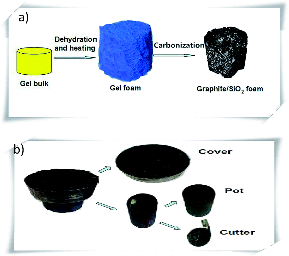 | ||
| Fig. 1 (a) Schematic of the synthesis of the graphite–SiO2 foam. (b) Schematic of the pot used for the synthesis of the graphite–SiO2 foam. | ||
The dehydrated gel was carbonized by heating it further at 250 °C for 5 hours. When the gel was heated, the wall and the cover of the pot forced the gel to form a cylinder and the hot air inside the pot blew the gel from time to time. Therefore, a porous foam was formed after this operation. This foam was first heated at 400 °C for 5 h and then at 1100 °C for 2 hours. It should be noted that the cooling process from 1100 °C to room temperature was set to be as fast as possible in order to prevent overheating of the samples. The typical cooling duration was around 4 hours. When the foam was cooled, the pot was taken out of the furnace. The steel cover was found to be adhered to the pot, and it was removed using a hammer. By rotating the cutter of the pot, the foam was taken out of the pot.
The resulting foam was characterized via X-ray powder diffraction (XRD), Raman spectroscopy, scanning electronic microscopy (SEM), soft X-ray absorption spectroscopy of the carbon and oxygen K-edges and silicon K-edge X-ray absorption near edge structure (XANES) spectroscopy. The experimental XRD profile is shown in Fig. 2, in which the phases of graphite are identified and crystalline phases of SiO2 are not observed. The phases of SiO2 were further confirmed to be amorphous in the silicon K-edge XANES spectra (Fig. 7), which will be discussed later.
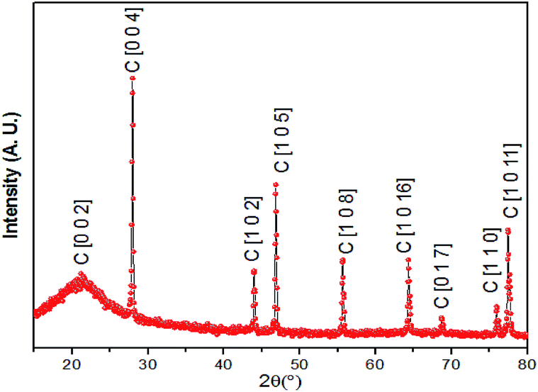 | ||
| Fig. 2 XRD pattern of the graphite–SiO2 composite foam. | ||
X-ray photoelectron spectroscopy (XPS) was applied to quantify the elements of the samples. The detailed quantification is listed in Table 1 and the XPS spectra are shown in Fig. 3. The XPS survey spectra are presented in the ESI.† The binding energy of C 1s of graphite, Si 2p of SiO2 and O 1s of SiO2 is 285.30 eV, 105.36 eV and 534.51 eV, respectively.
| Name | Peak BE | FWHM eV | Area (P) CPS eV | Atomic% |
|---|---|---|---|---|
| O 1s | 534.51 | 3.85 | 116![[thin space (1/6-em)]](https://www.rsc.org/images/entities/char_2009.gif) 562.69 562.69 |
48.24 |
| Si 2p | 105.36 | 3.97 | 22868.26 |
22.78 |
| C 1s | 285.30 | 2.77 | 29019.42 |
28.98 |
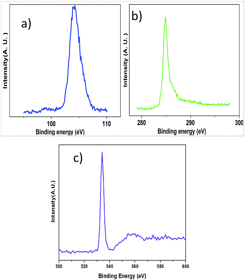 | ||
| Fig. 3 (a) XPS spectrum corresponding to Si 2p; (b) XPS spectrum corresponding to C 1s and (c) XPS spectrum corresponding to O 1s. | ||
Table presents details of the XPS parameters. The dominant element is found to be O 1s, and the atomic concentrations of Si 2p and C 1s are approximately equal.
The Raman spectra (Fig. 4) show prominent peaks at 190 cm−1, 412 cm−1, 451 cm−1, 583 cm−1, 794 cm−1, 921 cm−1, 1155 cm−1, 1329 cm−1, 1594 cm−1, 2543 cm−1 and 2658 cm−1. The sample exhibits the prominent peak of graphite at 1329 cm−1 (D peak), 1594 cm−1 (G peak) and 2658 cm−1 (G′ peak).34 The peaks at 190 cm−1, 412 cm−1, 451 cm−1 and 794 cm−1 are due to the vibrations of the Si–O bond.35,36 The peak at 921 cm−1 is associated with the Si–OH stretching mode (here, H element could be generated from the starting material, glucose).36 The peak at 583 cm−1 is attributed to the vibrations of the bridging oxygen in the Si–O–Si linkages.36 The peaks below 1500 cm−1 such as those at 1155 cm−1 and 1329 cm−1 are associated with the vibrational features of sp3 bonded carbons. The peak at around 2700 cm−1 (which is exactly at 2658 cm−1) is generally considered as the second order of the D peak or the 2D peak.34 The peaks at 1594 cm−1 and 2543 cm−1 are due to the defect states or the decomposition of the D peak and 2D peak of graphite. It should be mentioned that several sharp but weak Raman peaks appear at 486 cm−1, 492 cm−1, 496 cm−1, 503 cm−1, 516 cm−1, 521 cm−1, 524 cm−1, 530 cm−1 and 538 cm−1 (Fig. 4c). These peaks are due to the vibrations of O–B–O bending,37 which originates from the thermal decomposition of boric acid, one of the starting materials in the synthetic process.
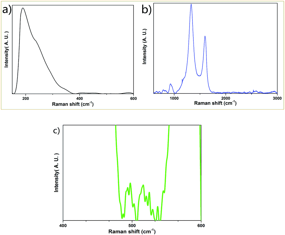 | ||
| Fig. 4 (a) Raman spectrum of the graphite–SiO2 composite foam in the range of 100 cm−1 to 600 cm−1. (b) Raman spectrum of the graphite–SiO2 composite foam in the range of 600 cm−1 to 3000 cm−1. (c) Non-prominent Raman peaks of the graphite–SiO2 composite foam in the range of 485 cm−1 to 540 cm−1. (The excitation wavelength was 632.80 nm). | ||
The surface morphology of the foam was characterized via SEM. During the imaging process, a 5 kV beam accelerating voltage was applied. The SEM image (Fig. 5a) shows the porous structure of the foam sample surface. The enlarged SEM image (Fig. 5b) clearly shows that the sample surface is rough.
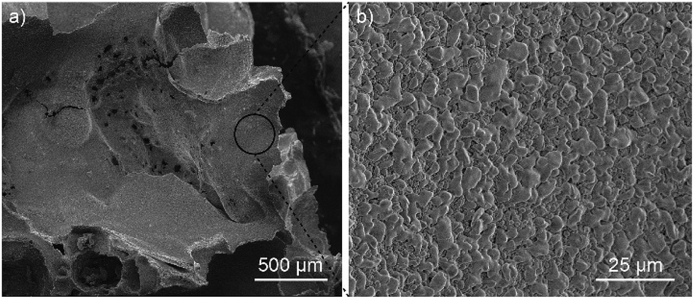 | ||
| Fig. 5 (a) SEM image of the graphite–SiO2 foam surface. (b) Enlarged SEM image of the region marked with a black circle in (a). The scale bars in (a) and (b) are 500 μm and 25 μm, respectively. | ||
Complementary to the X-ray photoelectron measurements of the occupied core electron states, XANES measurements allow the unoccupied states (partial density of electron states) of a sample to be probed. The carbon K-edge XANES spectra of the graphite–SiO2 foam and graphite foil were obtained and depicted in Fig. 6a. The two prominent peaks centered at 285.40 eV and 292.00 eV in the graphite foil absorption spectrum are resonances from the 1s → π* and 1s → σ* (sp2) electron transitions, respectively.38,39 With reference to the absorption spectrum of the graphite foil in Fig. 6a, it is clear that the graphite–SiO2 foam sample has the same transitions as the graphite foil. The strong peak from the 1s → π* transition indicates the graphitic structure of the graphite–SiO2 foam.
 | ||
| Fig. 6 (a) Carbon K-edge XANES spectra of graphite and the graphite–SiO2 foam and (b) oxygen K-edge XANES spectra of quartz and the graphite–SiO2 foam. | ||
It should be noted that the intensity of the shoulder and peak centered at around 288 eV between the π* and σ* transitions in Fig. 6a is enhanced. These features were reported in the previous work38,39 on graphite-related samples and were assigned to the 1s → π* transition from the C–O bond (286.00 eV) and the 1s → σ* transition (288.70 eV) from the aliphatic carbon and/or defect states. The X-ray photoelectron spectrum of the graphite–SiO2 foam (Fig. 3c) confirms C–O bond formation in the graphite–SiO2 foam as a shoulder located at 286 eV, which is attributed to the C–O functional group. Besides the carbon K-edge, we collected the oxygen K-edge absorption spectra of the graphite–SiO2 foam to gain further insight into its electronic structure.
The oxygen K-edge XANES spectra of the graphite–SiO2 foam and quartz reference sample are displayed in Fig. 6b. The red line of the quartz oxygen K-edge XANES spectrum centered at 537.60 eV originates from the transition of the 1s electron to 2p electron states hybridized with the silicon 3s and 3p states in the tetrahedrally coordinated SiO2. The pre-edge peak that is apparent from the main edge at 532.00 eV was observed in previous SiO2 studies and is considered to originate from the O 1s electron transition to the π* orbital states of O2.40
Comparing the structure and features of the oxygen K-edge spectrum of the graphite–SiO2 foam with that of quartz, we observed no significant differences between the two spectra. However, we noticed that the oxygen K-edge of the graphite–SiO2 foam shows smoother features in the post edge XANES region (above 540 eV) compared to the XANES spectrum of quartz. These findings indicate that the graphite–SiO2 foam possess some imperfections in its silicon dioxide layer. The silicon K-edge XANES spectra of the graphite–SiO2 foam (Fig. 7) also confirm the imperfection in the silicon dioxide layers of the composite.
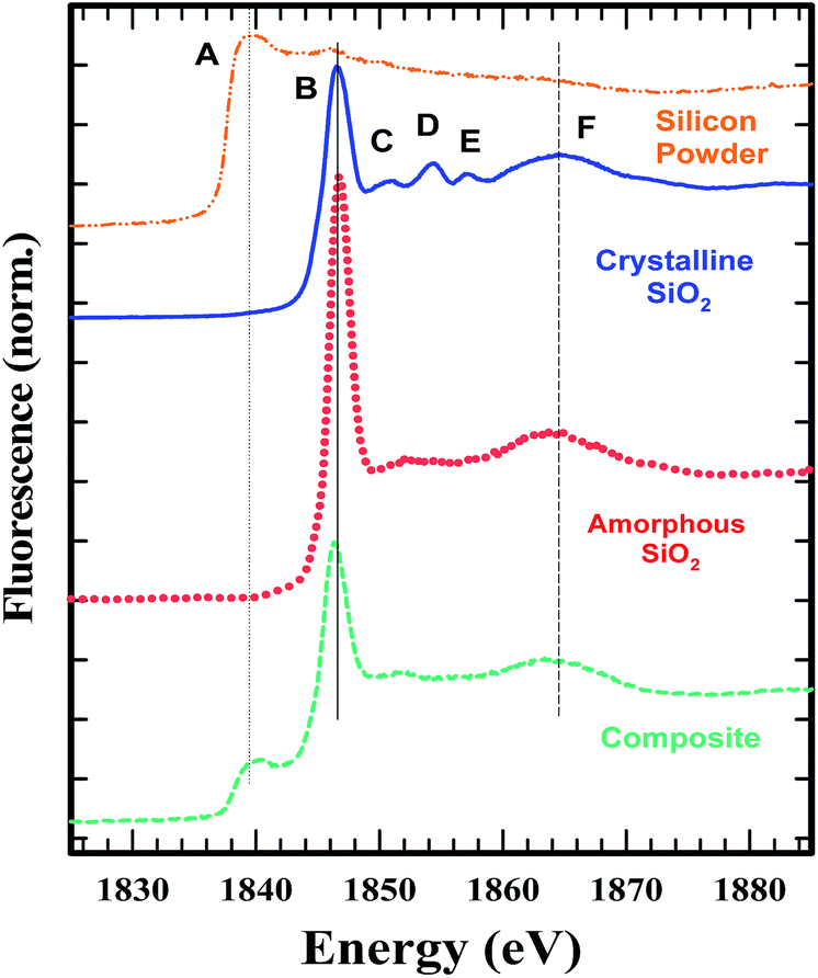 | ||
| Fig. 7 Silicon K-edge XANES of the graphite–SiO2 foam. | ||
Fig. 7 shows the Si K-edge XANES spectra of the graphite–SiO2 composite along with that of crystalline and amorphous SiO2 and a silicon powder. The comparison shows that the SiO2 in the composite is amorphous. The smaller D and E peaks seen in the crystalline SiO2 are absent in the composite, similar to the amorphous SiO2. The C peak, which is less pronounced, is present in the composite, similar to the amorphous silica. A comparison of the composite spectra with that of the silicon powder shows that some of the starting material remained in the sample.
Fig. 8 is the electrical measurement configuration. Silver gel was used in order to make close contact between the electrical wires and the sample.
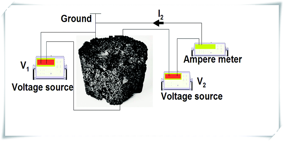 | ||
| Fig. 8 Electrical measurement diagram for the sample, where V1 and V2 are the applied voltage and I2 represents the current. | ||
As shown in Fig. 9, the current I2 increases with an increase in the voltage V2 (Fig. 9a), which satisfies Ohm's law. However, I2 decreases with an increase in the voltage V1 (Fig. 9b), which is indeed a negative resistance effect and contrary to Ohm's law.
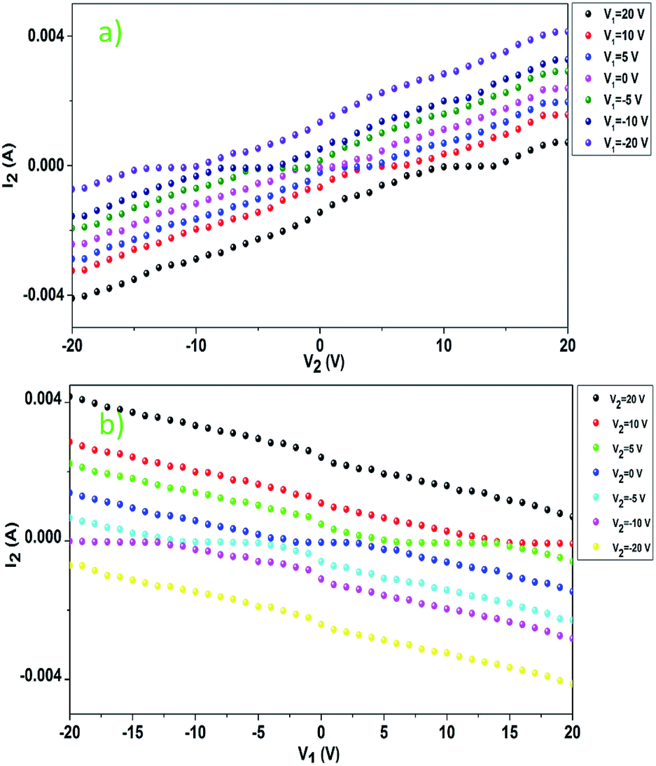 | ||
| Fig. 9 Current dependence on voltage: (a) I2 vs. V2 when V1 is different and (b) I2 vs. V1 when V2 is different. | ||
There is no decisive conclusion about the origin of the negative resistance effect, which is considered to be due to the potential barrier enhancement,25 excitation of the domain-wall,26 resonant tunneling,30 impurity band conduction,29 and construction of localized electrical polarization.33
In order to explain this effect, two possible mechanisms are proposed as follows.
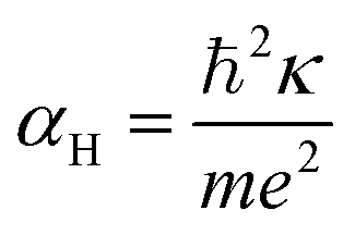
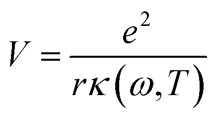
The first possible mechanism is due to the existence of defect states in the composite foam. As derived from Table 1, the atomic ratio of oxygen-to-silicon is 2.12, which indicates that O 1s is redundant. These redundant O 1s could combine with the small amount of the remaining starting materials (such as C and H from glucose and B from boron acid) to form a complex structure which is undetectable in the Raman/XANES spectra due to the resolution limitation of the instruments or appears as small peaks in the spectra profile. This is consistent with the findings from the Raman/XANES spectra. As mentioned in the paragraph describing the Raman spectra, the Raman peaks at 486 cm−1, 492 cm−1, 496 cm−1, 503 cm−1, 516 cm−1, 521 cm−1, 524 cm−1, 530 cm−1 and 538 cm−1 are attributed to the vibration of O–B–O bending and the peak at 921 cm−1 is considered due to the Si–OH stretching mode. Also, as stated in the XANES section, two peaks from XANES indicate the formation of C–O bond (286.00 eV)/defect states (288.70 eV). They are certain sources of defects existing in the composite foam. The dielectric constant for the electrons around these defects would be higher.41 The Bohr radius can be calculated as41
 | (1) |
 | (2) |
 | (3) |
Given that the permittivity is dependent on temperature, the potential is associated with the temperature. When an external voltage is applied on the sample, it causes the temperature to increase. Therefore, the potential is subjected to external modulation of the electrical voltage. In this way, the variation in the potential is introduced by voltage modulation. Interactions between the extra band and empty states of the atoms appear and some the electrons from the defects could transit between the extra band and the side of the atoms. Therefore, electric polarization appears in the extra band and electrical coupling is introduced (Fig. 10a).
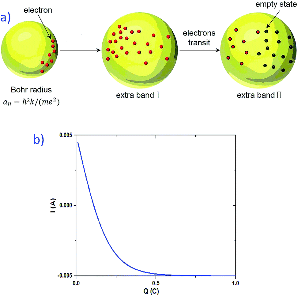 | ||
| Fig. 10 (a) Process for the formation of electrical coupling due to the existence of defect states. The electrons around the defect states first occupy the region with a higher Bohr radius and form an extra band. Then, the interactions between these electrons and the empty states of other atoms produce electrical polarization and electric coupling is introduced. (b) Simulated result of the current vs. charge shifting amount. | ||
If the direction of the electric polarization contributed from the extra band is in contrast to that of the electric field applied, it will harm the output current and even change its direction. When a higher electrical field is applied, the variation in potential becomes larger. At the same time, opposite electric polarization is introduced. Therefore, the output current becomes smaller. In this way, the negative resistance effect becomes active.
Another possible mechanism is the change in the charge shift amount (see the ESI for a detailed theoretical derivation†). When a voltage is applied to the sample, the charge shifts due to the existence of a localized electric field. The current derived is dependent on the amount of the charge that is shifted by the electrical field (see eqn (S.24) in the ESI†). Fig. 10b presents the simulated result of I vs. Q. The increase in the charge shifting amount leads to a decrease in the current, which is a possible explanation for the negative resistance effect in the graphite–SiO2 foam.
Experimental
Materials
The raw materials used to synthesize the graphite–SiO2 foam include melted-glucose (CK Products, LLC., USA), silicon powder (Johnson Matthey Catalog Company, USA) and boric acid (Fisher Scientific Company, Chemical Manufacturing Division, USA).SEM, XRD, XPS and Raman characterization
The prepared foams were studied via electron microscopy, Raman spectroscopy and X-ray diffraction. SEM was conducted using an FEI Quanta 200 SEM. Raman spectroscopy was performed using a Johin Yvon Horiba LABRAM Integrated Raman Spectroscopy System using an HeNe laser (wavelength: 632.81 nm). XRD patterns were collected using a Shimazu XRD-6000 with Cu Kα radiation of 1.5406 Å. XPS analyses were conducted using a K-α XPS instrument (Thermo Scientific, USA).Soft X-ray absorption spectroscopy of the carbon and oxygen K-edge
Soft X-ray absorption spectroscopy of the carbon and oxygen K-edges was performed at the variable-line-space plane-grating-monochromator (VLSPGM) beamline of the Center for Advanced Microstructures and Devices (CAMD), Louisiana State University, Baton Rouge, Louisiana, USA. The beamline that provides a resolution better than 0.20 eV at the carbon K-edge has been described in detail elsewhere.43 The soft X-ray beamline monochromator delivered monochromatic photons in the energy range of 180–1000 eV with two interchangeable gratings. We collected the absorption spectra using the total electron yield technique by measuring the sample's drain current with a 0.20 eV energy step size. The spectra were normalized to the primary beam current acquired from the gold sputtered mesh. The base pressure of the chamber was at 2 × 10⁻⁹ Torr. We exploited a graphite foil and powdered quartz reference samples to calibrate the energy scale of the grating and identify the absorption features on the graphite–SiO2 foam sample.Silicon K-edge XANES spectra measurement
Silicon K-edge XANES spectra of the composite and relevant silicon standards were measured at the Low Energy X-ray Absorption Spectroscopy (LEXAS) Beamline of J. Bennett Johnston, Sr. in CAMD. CAMD operates an electron storage ring at 1.30 GeV. LEXAS is a windowless beamline with only a 13 μm thin Kapton window separating the ring from the experimental station. Measurements were made using a University of Bonn modified LeMonnier-type double crystal monochromator. InSb 111 crystals were used at this energy. The scan boundaries were 1800 eV to 1830 eV with 0.50 eV steps, 1830 eV to 1870 eV with 0.10 eV steps, and 1870 eV to 1910 eV with 0.30 eV steps. The measurements conducted via fluorescence with an 80 mm2 Ketek™ silicon drift detector. The material was diluted with boron nitride to keep the detector dead time low. The high dead time reduced the white line intensity. The integration time was varied from 3 to 5 seconds to obtain appropriate counting statistics. At least two spectra were collected. Data were analyzed using a Demeter and Athena system.44Conclusions
A graphite–SiO2 composite foam was synthesized using glucose as a foaming agent. The fabricated graphite–SiO2 composite foam shows the negative resistance effect. This effect is considered to occur due to two possible mechanisms: (1) the existence of defect states and (2) change in the charge shifting amount. Due to the use of simple chemistry and the negative resistance effect, our technique may provide a rapid processing method to fabricate electric devices for a variety of macroelectronic applications.Conflicts of interest
There are no conflicts to declare.Acknowledgements
The authors thank the financial support from by Chongqing Research Program of Basic Research and Frontier Technology (No. cstc2017jcyjAX0469).References
- B. Sun and M. Skyllas-Kazacos, Electrochim. Acta, 1992, 37, 2549 CrossRef.
- T. W. Ebbesen, H. J. Lezec, H. Hiura, J. W. Bennett, H. F. Ghaemi and T. Thio, Nature, 1996, 382, 54 CrossRef CAS.
- R. A. Jishi, M. S. Dresselhaus and G. Dresselhaus, Phys. Rev. B, 1993, 48, 11385 CrossRef CAS.
- E. H. Hwang, S. Adam and S. Das Sarma, Phys. Rev. Lett., 2007, 98, 186806 CrossRef CAS PubMed.
- X.-C. Dong, H. Xu, X.-W. Wang, Y.-X. Huang, M. B. Chan-Park, H. Zhang, L.-H. Wang, W. Huang and P. Chen, ACS Nano, 2012, 6, 3206–3213 CrossRef CAS PubMed.
- X. Cao, Y. Shi, W. Shi, G. Lu, X. Huang, Q. Yan, Q. Zhang and H. Zhang, Small, 2011, 7, 3163–3168 CrossRef CAS PubMed.
- W. Chen, S. Li, C. Chen and L. Yan, Adv. Mater., 2011, 23, 5679–5683 CrossRef CAS PubMed.
- L. Zhang, F. Zhang, X. Yang, G. Long, Y. Wu, T. Zhang, K. Leng, Y. Huang, Y. Ma, A. Yu and Y. Chen, Sci. Rep., 2013, 3, 1408 CrossRef PubMed.
- W. Wei, S. Yang, H. Zhou, I. Lieberwirth, X. Feng and K. Müllen, Adv. Mater., 2013, 25, 2909–2914 CrossRef CAS PubMed.
- D.-W. Wang, F. Li, M. Liu, G. Q. Lu and H.-M. Cheng, Angew. Chem., Int. Ed., 2008, 47, 373–376 CrossRef CAS PubMed.
- P. S. Dorozhkin, S. V. Tovstonog, D. Golberg, J. Zhan, Y. Ishikawa, M. Shiozawa, H. Nakanishi, K. Nakata and Y. Bando, Small, 2005, 1, 1088–1093 CrossRef CAS PubMed.
- J.-M. Ting, T.-P. Li and C.-C. Chang, Carbon, 2004, 42, 2997–3002 CrossRef CAS.
- J. Ji, L. L. Zhang, H. Ji, Y. Li, X. Zhao, X. Bai, X. Fan, F. Zhang and R. S. Ruoff, ACS Nano, 2013, 7, 6237–6243 CrossRef CAS PubMed.
- J. Ji, H. Ji, L. L. Zhang, X. Zhao, X. Bai, X. Fan, F. Zhang and R. S. Ruoff, Adv. Mater., 2013, 25, 4673–4677 CrossRef CAS PubMed.
- X. Xia, D. Chao, Z. Fan, C. Guan, X. Cao, H. Zhang and H. J. Fan, Nano Lett., 2014, 14, 1651–1658 CrossRef CAS PubMed.
- D. Chao, X. Xia, J. Liu, Z. Fan, C. F. Ng, J. Lin, H. Zhang, Z. X. Shen and H. J. Fan, Adv. Mater., 2014, 26, 5794–5800 CrossRef CAS PubMed.
- J. Ji, J. Liu, L. Lai, X. Zhao, Y. Zhen, J. Lin, Y. Zhu, H. Ji, L. L. Zhang and R. S. Ruoff, ACS Nano, 2015, 9, 8609–8616 CrossRef CAS PubMed.
- Y. Chen, Z. Zhang, Z. Sui, Z. Liu, J. Zhou and X. Zhou, Int. J. Hydrogen Energy, 2016, 41, 12136–12145 CrossRef CAS.
- J. Tolvanen, J. Hannu, M. Nelo, J. Juuti and H. Jantunen, Smart Mater. Struct., 2016, 25, 1–12 CrossRef.
- Y. Tong, X. Yu and G. Shi, Phys. Chem. Chem. Phys., 2017, 19, 4821–4826 RSC.
- M. Inagaki, J. Qiu and Q. Guo, Carbon, 2015, 87, 128–152 CrossRef CAS.
- K. Prabhakaran, P. K. Singh, N. M. Gokhale and S. C. Sharma, J. Mater. Sci., 2007, 42, 3894–3900 CrossRef CAS.
- C. Wang, M. J. O'Connell and C. K. Chan, ACS Appl. Mater. Interfaces, 2015, 7, 8952–8960 CAS.
- Y. Yuan, Y. Ding, C. Wang, F. Xu, Z. Lin, Y. Qin, Y. Li, M. Yang, X. He, Q. Peng and Y. Li, ACS Appl. Mater. Interfaces, 2016, 8, 16852–16861 CAS.
- T. W. Hickmott, J. Appl. Phys., 1962, 33, 2669 CrossRef CAS.
- P. A. Lee, Solid State Commun., 1969, 7, 1359–1361 CrossRef CAS.
- S. Itoh, Y. Ohta and H. Fujiyasu, Appl. Phys. Lett., 1977, 31, 701–703 CrossRef CAS.
- Y. Iwasa, T. Koda, S. Koshihara, Y. Tokura, N. Iwasawa and G. Saito, Phys. Rev. B, 1989, 39, 10441 CrossRef.
- H. S. Majumdar, J. K. Baral, R. Osterbacka, O. Ikkala and H. Stubb, Org. Electron., 2005, 6, 188–192 CrossRef CAS.
- M. Tsuchiya, H. Sakaki and J. Yoshino, Jpn. J. Appl. Phys., 1985, 24, L466–L468 CrossRef.
- K. Ismail, W. Chu, A. Yen, D. A. Antoniadis and H. I. Smith, Appl. Phys. Lett., 1989, 54, 589–591 CrossRef.
- A. Yasuda, K. Suto and J.-i. Nishizawa, Results Phys., 2016, 6, 41–42 CrossRef.
- Y. Wu, H. Fu, B. Li and Y. Lin, Mater. Express, 2017, 7, 5–14 CrossRef CAS.
- S. Reich and C. Thomsen, Philos. Trans. R. Soc., A, 2004, 362, 2271–2288 CrossRef CAS PubMed.
- F. L. Galeener, J. C. Mikkelsen Jr, R. H. Geils and W. J. Mosby, Appl. Phys. Lett., 1978, 32, 34–36 CrossRef CAS.
- P. F. McMillan and R. L. Remmele Jr, Am. Mineral., 1986, 71, 772–778 CAS.
- R. R. Servoss and H. M. Clark, J. Chem. Phys., 1957, 26, 1175–1178 CrossRef CAS.
- Y. V. Fedoseeva, G. A. Pozdnyakov, A. V. Okotrub, M. A. Kanygin, Y. V. Nastaushev, O. Y. Vilkov and L. G. Bulusheva, Appl. Surf. Sci., 2016, 385, 464–471 CrossRef CAS.
- M. Abbas, Z. Y. Wu, J. Zhong, K. Ibrahim, A. Fiori, S. Orlanducci, V. Sessa, M. L. Terranova and I. Davoli, Appl. Phys. Lett., 2005, 87, 051923 CrossRef.
- G. S. Henderson, D. R. Neuville and L. Cormier, Chem. Geol., 2009, 259, 54–62 CrossRef CAS.
- N. F. Mott, Conduction in Noncrystalline Materials, Clarendon, Oxford, 1987 Search PubMed.
- Z.-Y. Cheng, R. S. Katiyar, X. Yao and A. S. Bhalla, Phys. Rev. B, 1998, 57, 8166–8177 CrossRef CAS.
- M. Ono, J. D. Scott and E. Morikawa, AIP Conf. Proc., 2004, 705, 364 CrossRef.
- B. Ravel and M. Newville, J. Synchrotron Radiat., 2005, 12, 537–541 CrossRef CAS PubMed.
Footnote |
| † Electronic supplementary information (ESI) available. See DOI: 10.1039/c7ra07465d |
| This journal is © The Royal Society of Chemistry 2017 |