
 Open Access Article
 This Open Access Article is licensed under a Creative Commons Attribution-Non Commercial 3.0 Unported Licence
Space charges and negative capacitance effect in organic light-emitting diodes by transient current response analysis
Min Guan *a,
Litao Niua,
Yang Zhang*b,
Xingfang Liua,
Yiyang Lia and
Yiping Zenga
*a,
Litao Niua,
Yang Zhang*b,
Xingfang Liua,
Yiyang Lia and
Yiping Zenga
aKey Laboratory of Semiconductor Material Sciences, Beijing Key Laboratory of Low Dimensional Semiconductor Materials and Devices, Institute of Semiconductors, Chinese Academy of Sciences, Beijing 100083, People’s Republic of China. E-mail: guanmin@semi.ac.cn; Fax: +86-10-82304232; Tel: +86-10-82304101
bCollege of Materials Science and Optoelectronic Devices, University of Chinese Academy of Sciences, Beijing 100049, People’s Republic of China. E-mail: zhang_yang@semi.ac.cn; Fax: +86-10-82304232; Tel: +86-10-82304101
First published on 31st October 2017
Abstract
Space charge capacitance and the physical mechanism of negative capacitance in organic light-emitting diodes (OLEDs) by transient current response analysis are investigated for the first time. Space charge capacitance is found to be a fixed value as voltage increases for each device. The inflection points in capacitance–voltage curves correspond to carrier injection, transportation and combination processes in organic layers. A negative capacitance effect at low frequency relates to the internal accumulated carrier state in the OLEDs. The nonsynchronicity between the phases of the internal accumulated carriers’ states changing and the small alternating current leads to electric field reversal. Only the electric field reversal at low frequency results in a negative capacitance effect.
Introduction
Due to their high efficiency, fast response, richness of color, wide view angle and flexible characteristics, organic light-emitting diodes (OLEDs) have been used in small area consumer product displays, panel display equipment and some emergency response equipment. Therefore, they have attracted wide investigation interest around the world.1–13 Capacitance (C) characteristics can provide a powerful method to understand the physical mechanisms of OLEDs. Negative capacitance (NC) is one of the most notable phenomena in OLEDs. The effects of the hole injection barrier, measurement frequency and device structure on OLED capacitance have been reported.14–22 The inflection points of capacitance–voltage (C–V) curves have been reported to be influenced by the device structure to some degree. Juan Bisquert16 reported that the negative capacitance effect in OLEDs is induced by sequential electron injection at the organic/metal interface. The electron is injected into states in the bandgap in the dipole layer at first and then into bulk states. However, Wei-Chih Chen23 attributed the negative capacitance to the synchronized occurrence of interconversion of different parts of organic materials. Detailed physical mechanisms of C–V and NC characteristics are still not fully understood. The relationship between capacitance and carrier transportation also needs deeper investigation.In our previous investigations, transient current response characteristics of OLEDs were found to be related to the space charges near electrodes.24 The space charges charging and discharging processes result in capacitance characteristics. Therefore, in this paper, we will investigate the capacitance characteristics with transient current response. The relationships between capacitance, space charges, charge transportation and measurement frequency are investigated at first. Then, we provide a conjecture for the NC physical mechanism.
Experiments
To analyse the capacitance characteristics, four OLED devices were designed and fabricated in this work. The devices were made as follows. Firstly, indium-tin-oxide (ITO)-coated glass substrates were treated with O3 for 15 min. Thereafter, organic layers were deposited on the substrates in an organic molecular beam deposition (OMBD) system with a vacuum of 5.0 × 10⁻⁸ Torr. LiF and Al cathode were deposited on top of the organic stack. The materials used in this work were MoO3, N,N′-diphenyl-N,N′-bis(1-naphthyl)-1,1′-biphenyl-4,4′-diamine (NPB), fac-tris(2-phenylpyridine) iridium doped 4,4′-bis(N-carbazolyl)-1,1′-biphenyl ([Ir(ppy)3:CBP], 12 wt%), 2,9-dimethyl-4,7-diphenyl-1,10-phenanthroline (BCP), tris(8-hydroxyquinoline) aluminum (Alq3) and 10-(2-benzothiazolyl)-2,3,6,7-tetrahydro-1,1,7,7-tetramethyl-1H,5H,11H-(1)benzopyropyrano(6,7-8-I,j)quinolizin-11-one doped Alq3 (C545T:Alq3, 0.68 wt%). The light emitting area of all of the devices is 1 mm2. Device structures are listed in Table 1.| Device | Structure |
|---|---|
| D1 | ITO/MoO3 5 nm/NPB 70 nm/Alq3 60 nm/LiF 1 nm/Al 120 nm |
| D2 | ITO/MoO3 5 nm/NPB 70 nm/Ir(ppy)3:CBP 20 nm/BCP 10 nm/Alq3 20 nm/LiF 1 nm/Al 120 nm |
| D3 | ITO/MoO3 5 nm/NPB 70 nm/C545T:Alq3 20 nm/BCP 10 nm/Alq3 20 nm/LiF 1 nm/Al 120 nm |
| D4 | ITO/MoO3 5 nm/NPB 55 nm/Alq3 5 nm/NPB 5 nm/Alq3 5 nm/NPB 5 nm/Alq3 5 nm/NPB 5 nm/Alq3 45 nm/LiF 1 nm/Al 120 nm |
The luminance–voltage (L–V) characteristics of these devices were measured using a Keithley electrometer 2400 and ST-86LA spot photometer. A pulsed voltage with less than 20 ns rise time was generated by a SYSTRON DONNER MODEL 110D Pulsed Generator. A 50 Ω current sensing resistor was connected in series with the OLED device to capture the current response. A RIGOL DS1062CA oscilloscope was used to capture the voltage loaded on the current sensing resistor. The response speed of the pulsed generator and the oscilloscope are sufficiently fast. The C–V characteristics were measured by an Agilent B1500A Semiconductor Device Analyzer.
Results and discussion
As is known to all, a space charge limited current is formed in OLEDs. The charging and discharging process of space charges results in a capacitance effect in OLEDs. For the purpose of calculating the space charge capacitance, we should know the amount of space charge formed in these devices. Therefore, we measured the transient current response characteristics. A typical transient current response curve of an OLED is depicted in Fig. 1 inset. Evidently, the transient current response curve can be divided into three parts: the positive current spike when the pulsed voltage is switched on, a small steady-state current and an immediately larger negative current spike after the pulse voltage is switched off. A larger negative spike than positive spike could be found in all devices. This is because there is a hole injection energy barrier from the anode to the NPB when the pulsed voltage is started. However in the discharging process, holes diffuse from the NPB to the anode with no energy barrier, leading to a larger transient current than in the charging process.24 Both the positive and negative current peaks can be used to calculate the amount of space charges. For the positive IS, it is not easy to decide on the range of integration of the positive current peak. In order to improve the accuracy, we integrated the negative current peak instead of the positive current peak. Fig. 1 depicts the integration area of the current curve following the equation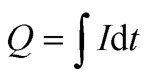 . Here Q, I and t are the amount of space charges, current and time respectively. Then the space charge capacitance is calculated following the function C = Q/V. Here C, Q and V are the space charge capacitance, the amount of space charge and the pulsed voltage, respectively. The calculated space charge capacitance characteristics with pulsed voltage are shown in Fig. 2(a) inset.
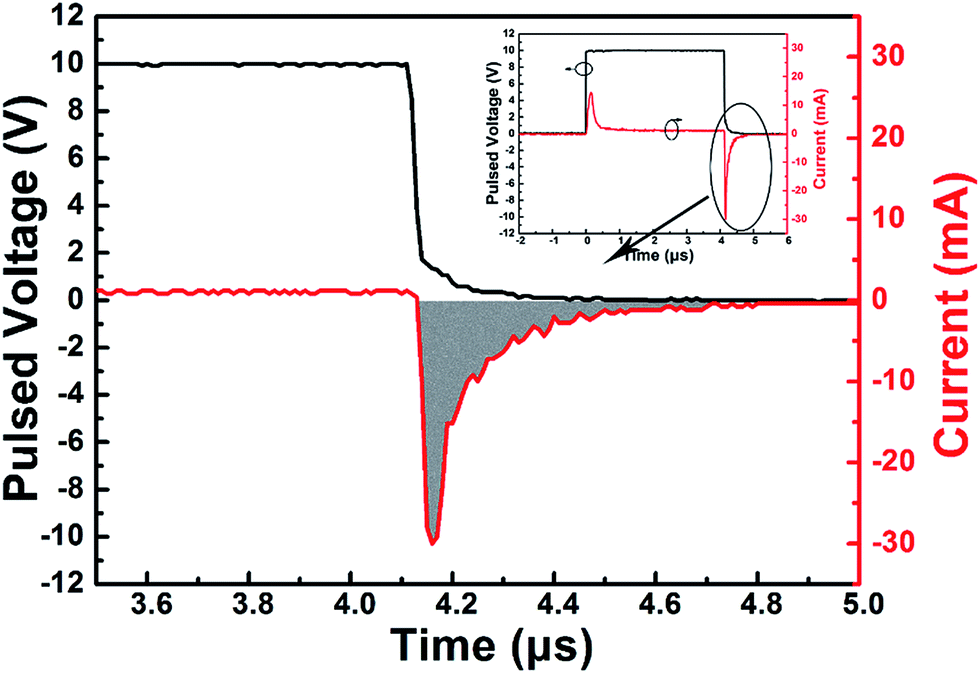 | ||
| Fig. 1 Diagrammatic sketch of the current integration area. Inset: a typical OLED current response curve under pulsed voltage. | ||
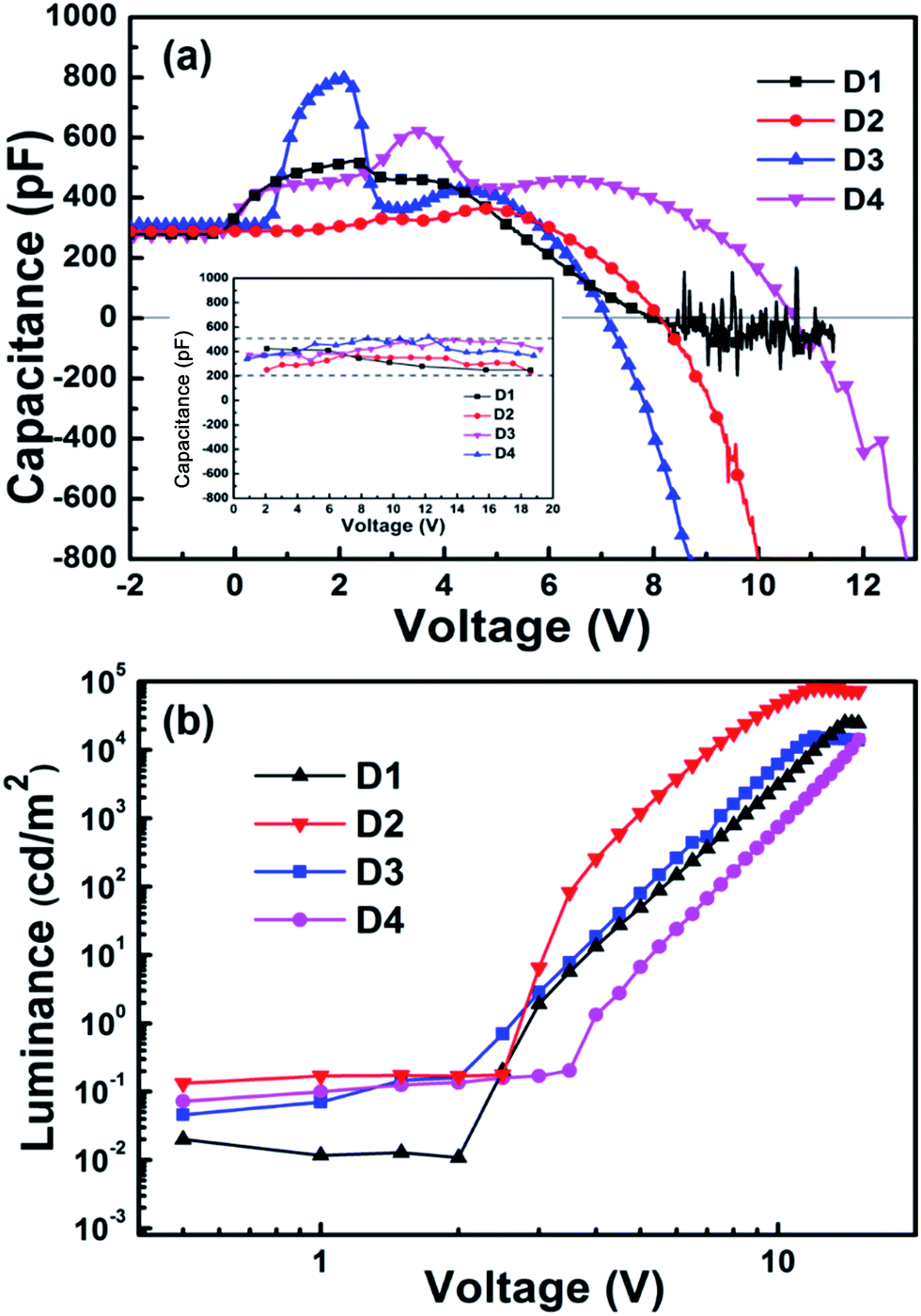 | ||
| Fig. 2 Capacitance characteristics and luminance of OLEDs: (a) C–V characteristics of OLEDs (frequency is 1 kHz); inset: calculated space charge capacitance based on the current response curve; (b) L–V characteristics of OLEDs. | ||
Due to the varying accuracy at different ranges of the RIGOL DS1062CA oscilloscope, the calculated space charge capacitance curves of the four devices are tortuous. However, for each device, with the increase of the pulsed voltage, the calculated capacitance values basically do not change much. The differences between the maximum and minimum values are smaller than 150 pF, as depicted in Fig. 2(a) inset. To compare with the C–V curves measured using the Agilent B1500A, the difference in the space charge capacitance can be ignored. Therefore, the space charge capacitance can be treated as a fixed value for each device. The fixed value can be considered as equal to the capacitance at negative voltage measured using the Agilent B1500A. For example, as shown in Fig. 2(a), at 0 V, the test capacitances of the four devices are 280, 290, 275 and 310 pF respectively. For each device, this value is related to the thickness of the entire organic layer of the device. Although the structures are different, the total organic layer thickness of each device is about 130 nm. It is known to all that space charges can have several origins: injected charges, ionized dopants, mobile ions etc. Traps formed on the electrode interface will reduce the mobility and thus may contribute to the space charge. In addition to the calculation error, these values and the calculated capacitance values from the transient current response are in a range. The slight difference in space charge at different voltages may be due to the trap-assisted space charge being neglected in a first order approximation. Summing up the above results, we consider that the simulated capacitance from the transient current response peak represents the space charge capacitance effect before the device emits light.
To further investigate the capacitive effect, we tested the capacitance–voltage performance of the four devices. The capacitances of the four devices at 1 kHz measured using the Agilent B1500A are depicted in Fig. 2(a). Differing from the simulated capacitance from the transient current response, the test capacitance is fixed at 300 pF when the driving voltage is negative. It should be noted that some peak capacitance appears with the increasing voltage. However, after several inflection points, the capacitance changes from positive to negative values at high voltage. Fig. 2(b) depicts the luminance–voltage (L–V) characteristics of the four devices, at a steady state voltage. In the L–V log coordinates curves, there are significant inflection points which correspond to the devices’ turn-on voltages. When the device brightness is 1 cd m−2, we can see that the turn-on voltages are 2.6 V, 2.7 V, 3.6 V and 4.4 V for devices 1, 2, 3 and 4 respectively. It is found that the turn-on voltage of a device is the same as the voltage of the first inflection point in the C–V curve, for all devices. This implies that the C–V curve inflection points should be induced by charge transportation in the organic layers.
After the voltage changes from negative to positive values, the carriers begin to be injected in the OLEDs. Due to the lower injection barrier for holes than electrons, holes will be injected first. Due to there being no electron injection, the injected holes will accumulate on the internal organic layer interfaces, as depicted in Fig. 3. OLED devices are surface-emitting and constructed of several organic layers. Therefore, OLED capacitance is similar to that of a parallel-plate capacitor. Capacitance can be calculated following the equation of C = εε0S/d. Here C is capacitance, ε relative permittivity of the organic materials, ε0 vacuum permittivity, S surface area and d organic thickness. For device 1, when the holes accumulate on the MoO3/NPB internal interface, the shortening of the effective distance results in a higher C value. With increasing voltage, electrons begin to be injected from the cathode and combine with the accumulated holes on the NPB/Alq3 interface inducing a decrease in the accumulated holes. As the accumulated holes continue to be consumed, the capacitance value will decrease forming the first decreasing inflection point in the C–V curve. Unlike for device 1, the other three devices have different degrees of multiple inflection points in their C–V curves. For instance, there are two rising inflection points before the first decreasing inflection point appears for device 4. This is induced by the multi-well structure. As depicted in Fig. 3(a)–(c), there are more hole accumulating interfaces before combination with the electrons, resulting in more rising inflection points. At higher voltage, before capacitance decreases seriously, the trend of the C–V curve should be affected by the carriers’ injection rate and consumption rate. C will increase if the carriers’ injection rate is faster than the consumption rate. As the voltage continued to increase in these devices, the phenomenon of negative capacitance (NC) appeared.
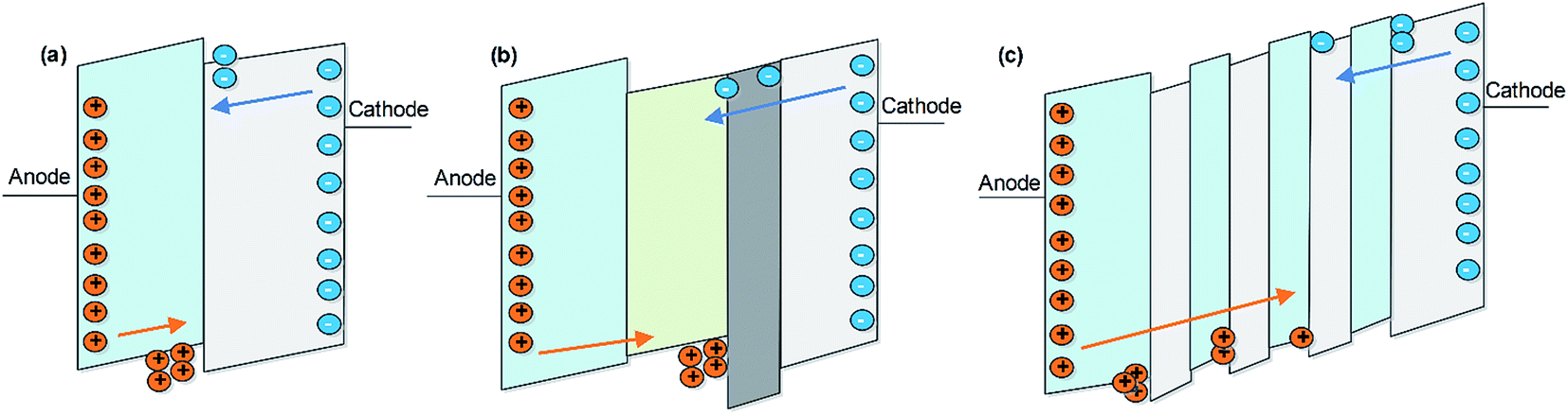 | ||
| Fig. 3 Schematic diagram of charge distribution in the organic layers before hole and electron combination. (a) Charge distribution in device 1; (b) charge distribution in devices 2 and 3; (c) charge distribution in device 4. | ||
In order to have a deep insight into the mechanism of NC, we investigated the variation of the capacitance with the voltage at different AC signal frequencies. As shown in Fig. 4(a)–(d), with the increase of AC signal frequency from 1 kHz to 50 kHz, the inflection points of the capacitance curves obviously weaken or disappear for the devices. At the same time, the negative capacitance effect at high voltage is also weakened. At high frequencies, the AC signal changed very quickly, while the carrier migration rate in the organic materials was slower than that for the inorganic materials, such that the change of carrier transport state is difficult to match with the change of the AC signal. Because of this, the charge is difficult to accumulate and consume in the different interface layers of the OLEDs. However, there are no such significant changes with frequency in inorganic device C–V curves. Therefore, we attribute the weak inflection phenomenon at high frequency to low carrier mobility in organic layers.
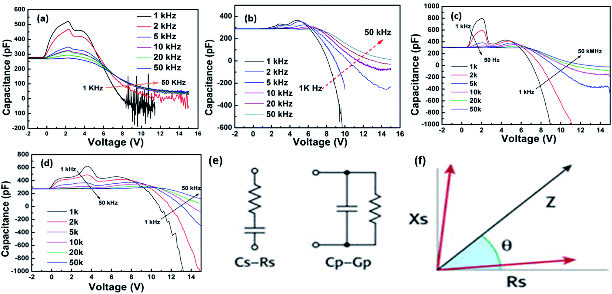 | ||
| Fig. 4 C–V curves of the devices at different frequencies and measurement parameters: (a)–(d) C–V curves at different frequencies of the four devices respectively; (e) parallel and series capacitance measurement methods; (f) the relationship between impedance (Z), phase angle (θ), reactance (XS) and resistance (RS). | ||
Generally speaking, as shown in Fig. 4(e), there are two capacitance measurement methods: parallel and series measurement methods. The space charge capacitance value is a fixed value for all devices. Therefore, the space charge capacitance will not induce NC in either measurement method. Fig. 4(f) depicts the relationship between impedance (Z), phase angle (θ), reactance (XS) and resistance (RS). Furthermore, the parameters follow the equations:
XS = Z![[thin space (1/6-em)]](https://www.rsc.org/images/entities/char_2009.gif) sinθ sinθ |
| CS = 1/(2πfXS) |
| CP = CS/(1 + D2) |
We can easily know if CP is negative; CS must be negative. Furthermore, XS must be negative. XS is defined as the opposition to a change in voltage due to capacitance (capacitive reactance) or in current due to inductance (inductive reactance). Therefore, a negative XS means that the capacitance reactance or inductive reactance will promote a change in voltage. The promotion of AC can be induced by the internal accumulated carriers. In our previous investigation on transient electroluminescence,25 we proved that there are large amounts of unconsumed carriers accumulated at internal interfaces. The small part of accumulated carriers’ (SPAC) states will change with the small AC signal in the C–V measurement process. However, due to the low mobility of the carriers in organic layers, the carriers’ states changing phase angle could not be synchronous with the small AC signal as we mentioned above. Therefore, the changing carriers’ states will fall behind the AC phase, leading to a negative phase angle between the phases of the changing carriers’ states and the AC phase. The electric field formed by SPAC will promote the alternating current. We have defined the phenomenon as the electric field reversal (EFR) effect. Because of the short cycle time, the changing carriers’ states will decrease significantly with increasing AC frequency. The EFR effect can be ignored, leading to the NC effect disappearing at high frequency. Therefore, we conclude that the NC phenomenon is induced by the nonsynchronicity between internal accumulated carriers’ states changing phase and AC changing phase.
Conclusions
In conclusion, capacitance characteristics of OLEDs have been thoroughly investigated. Space charge capacitance is found to be a fixed value for each device. The inflection points in C–V curves correspond to carrier injection, transportation and combination processes in organic layers at relative low frequency. Low carrier mobility in organic materials leads to weakened inflection phenomena at a high frequency small alternating current. However, at higher voltage, the capacitance will be mainly influenced by the internal accumulated carriers’ transport state. The nonsynchronicity between the phases of the internal accumulated carriers’ states changing and the small alternating current leads to an electric field reversal phenomenon. The electric field reversal phenomenon results in negative capacitance at low AC frequency, which can be ignored at high AC frequency.Conflicts of interest
There are no conflicts to declare.Acknowledgements
The authors acknowledge the support from the National Key Research and Development Program of China (2017YFB0405400), National Natural Science Foundation of China (Grant No. 61274049, 61404130 and 61574140), and Open Research Fund Program of the State Key Laboratory of Virology of China (2017IOV002).References
- H. Okumoto and T. Tsutsui, Appl. Phys. Express, 2014, 7, 061601 CrossRef.
- Y.-H. Deng, X.-Y. Chen, Q.-D. Ou, Q.-K. Wang, X.-C. Jiang, D.-D. Zhang and Y.-Q. Li, Appl. Phys. Lett., 2014, 104, 221104 CrossRef.
- M.-T. Hsieh, M.-H. Ho, K.-H. Lin, J.-F. Chen, T.-M. Chen and C. H. Chen, Appl. Phys. Lett., 2010, 96, 133310 CrossRef.
- Y. Chen, J. Chen, D. Ma, D. Yan and L. Wang, J. Appl. Phys., 2011, 110, 074504 CrossRef.
- A. P. Marchetti, T. L. Haskins, R. H. Young and L. J. Rothberg, J. Appl. Phys., 2014, 115, 114506 CrossRef.
- J. H. Wemken, R. Krause, T. Mikolajick and G. n. Schmid, J. Appl. Phys., 2012, 111, 074502 CrossRef.
- J. Liu, S. Huang, X. Shi, X. Wu, J. Wang and G. He, J. Phys. Chem. C, 2013, 117, 13887–13893 CAS.
- X.-W. Zhang, J.-W. Xu, H.-R. Xu, H. Wang, C.-L. Xie, B. Wei, X.-Y. Jiang and Z.-L. Zhang, J. Phys. D: Appl. Phys., 2013, 46, 055102 CrossRef.
- H. Hrichi, K. Hriz, M. Benzarti-Ghédira, N. Jaballah, R. Ben Chaâbane, M. Majdoub and H. Ben Ouada, Mater. Sci. Semicond. Process., 2013, 16, 851–858 CrossRef CAS.
- S. Chen, X. Jiang and F. So, Org. Electron., 2013, 14, 2518–2522 CrossRef CAS.
- J. Bisquert, Phys. Chem. Chem. Phys., 2008, 10, 3175–3194 RSC.
- W. Hu, Y. T. Tao and H. Sirringhaus, Phys. Chem. Chem. Phys., 2012, 14, 14097–14098 RSC.
- B. Minaev, G. Baryshnikov and H. Agren, Phys. Chem. Chem. Phys., 2014, 16, 1719–1758 RSC.
- L. S. C. Pingree, B. J. Scott, M. T. Russell, T. J. Marks and M. C. Hersam, Appl. Phys. Lett., 2005, 86, 073509 CrossRef.
- L. Zhang, H. Nakanotani and C. Adachi, Appl. Phys. Lett., 2013, 103, 093301 CrossRef.
- J. Bisquert, G. Garcia-Belmonte, Á. Pitarch and H. J. Bolink, Chem. Phys. Lett., 2006, 422, 184–191 CrossRef CAS.
- M. Terai, K. Fujita and T. Tsutsui, Jpn. J. Appl. Phys., Part 1, 2005, 44, L1059–L1062 CrossRef CAS.
- V. Shrotriya and Y. Yang, J. Appl. Phys., 2005, 97, 054504 CrossRef.
- J. M. Montero, J. Bisquert, G. Garcia-Belmonte, H. J. Bolink and E. M. Barea, Phys. Status Solidi A, 2007, 204, 2402–2410 CrossRef CAS.
- G. Garcia-Belmonte, H. J. Bolink and J. Bisquert, Phys. Rev. B: Condens. Matter Mater. Phys., 2007, 75, 085316 CrossRef.
- H. L. Kwok, Solid-State Electron., 2003, 47, 1089–1093 CrossRef CAS.
- M.-N. Tsai, T. C. Chang, P.-T. Liu, C.-W. Ko, C.-j. Chen and K.-m. Lo, Thin Solid Films, 2006, 498, 244–248 CrossRef CAS.
- W.-C. Chen, T.-C. Wen and A. Gopalan, Synth. Met., 2002, 128, 179–189 CrossRef CAS.
- L. Niu, M. Guan, X. Chu, Y. Zeng, Y. Li and Y. Zhang, J. Phys. Chem. C, 2015, 119, 10526–10531 CAS.
- L. Niu, M. Guan, X. Chu, Y. Zeng, Y. Li and Y. Zhang, J. Phys. D: Appl. Phys., 2015, 48, 055103 CrossRef.
| This journal is © The Royal Society of Chemistry 2017 |