
 Open Access Article
 This Open Access Article is licensed under a Creative Commons Attribution-Non Commercial 3.0 Unported Licence
The size controlled synthesis of Cu2S/P25 hetero junction solar-energy-materials and their applications in photocatalytic degradation of dyes
Hongqin Huanga,
Fang Lia,
Huigang Wang *ab and
Xuming Zhengab
*ab and
Xuming Zhengab
aDepartment of Chemistry, State Key Laboratory of Advanced Textiles Materials and Manufacture Technology, Ministry of Education, Zhejiang Sci-Tech University, Hangzhou 310018, China. E-mail: zdwhg@163.com; huigwang@uni-osnabrueck.de; Fax: +86-571-8684-3627; Tel: +86-571-8684-3627
bZhejiang Provincial Top Key Academic Discipline of Chemical Engineering and Technology, Zhejiang Sci-Tech University, Hangzhou 310018, China
First published on 27th October 2017
Abstract
In this paper highly dispersed Cu2S nanocrystals loaded on commercially available TiO2 form P25, denoted as Cu2S/P25, was firstly fabricated by a deposition–precipitation process, to establish close pn hetero junctions to improve the visible light activity and the stability of Cu2S on the catalyst surface. The catalysts were characterized by TEM, SEM, XRD, XPS, Raman, etc., the photocatalytic degradation kinetics of Cu2S-loaded TiO2 nanoparticles on methylene blue was systematically investigated. The results show that a lower amount of loading of Cu2S on Cu2S/P25 led to a higher photocatalytic degradation performance under visible light irradiation. The Cu2S quantum size effects on the absorption band edge and photo induced catalytic performance were also investigated.
1. Introduction
Methods to harvest sunlight radiation with a higher conversion efficiency to chemical or electrical power are needed to satisfy the demands of clean and green energy.1–4 For irradiation under light with a given wavelength, semiconductors with a specific band gap can resonate with the given light and produce electrons and holes, consequently generating active hydroxyl radicals in solution.5,6 These active hydroxyl radicals can degrade organics and kill microorganisms by advanced oxidation processes.7,8 Many semiconductors have been tested and TiO2 is a proverbial semiconductor with the advantages of high photocatalysis activity, wide band gap (3.2 eV), high earth abundancy, chemical stability and environmental friendliness.9–11 Photodegradations based on TiO2 and its hetero junction materials have attracted great attention in these decades due to their obvious advantages on the visible-light driven solar energy utilization.12,13 Various nanostructured hetero junctions have been reported and their enhanced photocatalytic efficiency has been achieved. For example, composites of MoS2–TiO2,14 SnO2–TiO2,15,16 CeO2–Cu2O17 and ZnO–TiO2,18–20 etc. have been synthesized by coupling two semiconductors.Chalcocite (Cu2S) is a p-type semiconductor for abundance in copper vacancies with a narrow bulk band gap of 1.2 eV.21–23 Further combining with n-type TiO2 by forming heterostructured nanocrystals would therefore be interesting in regard to achieving special properties, especially in photo degradation applications.12,13 In addition, the bandgap of Cu2S semiconductors and its characteristic absorption spectrum in the visible wavelength region make it highly desirable for use as sensitizers when they are combined with the TiO2 nanocrystals. On the other hand semiconductors with band gaps capable of harvesting visible incident wavelength energy (0.9 to 2.3 eV) usually suffer from UV induced photocorrosion, the stability of Cu2S under solar spectrum incidence thereof could be significantly enhanced by the formation of hetero junctions that could rapidly remove the photon-generated electrons and holes from the cuprous sulfide.24–26 Enhanced chemical stability, improved charge separation and increased photocatalytic efficiency of such composite nanostructures have been extensively studied by our group.6,27–31 In recent years of particular interest are the size dependent properties such as size quantization effects in semiconductor nanoparticles. Due to the quantum-confinement and surface effects, nanometer-sized semiconductors possess unique size-dependent physiochemical properties that one does not see in the corresponding bulk solids.32,33 The ability to synthetically tune these nanocrystal sizes provides the opportunity to study and understand the relationship between spectrum character, photo degradation performance and quantum effects that occur uniquely at the nanoscale. In addition, these nanocrystal dots open up new ways to utilize hot electrons or generate multiple electron–hole pairs with a single photon.34–36 Multiple electron–hole pairs generation in PbS nanocrystals-TiO2 single crystals has shown that photocurrents with quantum yields greater than one electron per photon can be achieved with a single high-energy photon.37
The purpose of this work was to know how and what the extent the quantum confinement of Cu2S effect on the visible light catalytic performance when it is coated onto the surface of TiO2 particles. In the present work, a series of different Cu2S size were achieved precipitated on P25 by deposition–precipitation process and their size effect on the absorption band edge and the catalytic performance were systematically investigated. By change the P25 quantity the Cu2S loading amount effects on the morphology and photocatalytic performance were also investigated. The photocatalytic degradation performance of the hetero structure catalysts was evaluated using methylene blue (MB) as a model pollutant. This dye is non-biodegradable and commonly used in the textile industry. As a result, this molecule is widely used for testing photocatalytic activity.
2. Experimental sections
2.1 Synthesis of Cu2S/P25 composites with deposition–precipitation method
To systematically investigate the synthesis condition and the relationship with the photocatalysis performance, the reactant amounts were varied, which are listed in Table 1. In a typical synthesis of Cu2S/P25 composites, Cu(Ac)2·H2O (0.2 g, 1 mmol) and 0.72 g P25 were added to the mixture of dodecanethiol and 1-octadecene (30 mL) in a three-necked flash under N2 atmosphere. Then it was heated to 220 °C and maintained at that temperature for 30 min after reaction, it was cooled to room temperature naturally. The product was precipitated by introducing ethanol and centrifuging at 9000 rpm. The precipitate was washed several times with ethanol and was dried under vacuum at a temperature of 60 °C for 12 h.| Sample | Copper acetate/g | P25/g | Dodecanethiol (mL) | 1-Octadecene (mL) |
|---|---|---|---|---|
| S1 | 0.2 | 0.40 | 30.00 | 0 |
| S2 | 0.2 | 0.72 | 30.00 | 0 |
| S3 | 0.2 | 1.12 | 30.00 | 0 |
| S4 | 0.2 | 2.56 | 30.00 | 0 |
| S5 | 0.2 | 0.72 | 15.00 | 15.00 |
| S6 | 0.2 | 0.72 | 5.00 | 25.00 |
| S7 | 0.2 | 0.72 | 0.75 | 29.25 |
2.2 Characterization
The morphologies of Cu2S and Cu2S/P25 were examined by a field-emission scanning electron microscope (FE-SEM, Hitachi S4800) and a transmission electron microscope (TEM, JEM 2100). The crystalline structure of samples was measured by X-ray diffraction (DX-2700). UV-visible diffuse reflectance spectra (DRS) of samples were recorded using a UV-vis NIR spectrophotometer (Varian Cary 5000). X-ray photoelectron spectroscopy (XPS) measurements were examined on Kratos AXIS Ultra DLD (Al Kα monochromatic source). Adventitious C 1s peak (284.6 eV) was used as binding energies reference. The 488 nm laser excited Raman spectra were measured on a quartz sheet equipped with triplemonochromator (TriVista TR557, Princeton Instruments) and an argon ion laser (approximately 30 mW on the sample). The CCD chip active area covers a wavenumber of 1089 cm−1 and the spectral resolution boasts for 2.5 cm−1.2.3 Photocatalytic activity measurements
The photocatalytic activity of Cu2S/P25 samples was evaluated by the degradation rate of methylene blue under visible-light irradiation. The experimental set up placed in a black box consisted of a 200 mL beaker irradiated by a 300 W, 220 V xenon lamp (CEL-HXUV300, Beijing Au Light). The distance between the lamp and the solution is 15 cm. The temperature inside the reactor was maintained at ca. 25 °C by means of a continuous circulation of water surrounding the reactor. 100 mL methylene blue (MB) aqueous solution (10 mg L−1) was mixed with 50.0 mg photocatalyst powder in the above 200 mL beaker. Before irradiation, the suspension was stirred in the black box for about 30 min till to reach the adsorption–desorption equilibrium. After the photoreaction runs, samples of 3 mL were withdrawn from the suspension at regular time intervals during the irradiation, and then centrifuged to separate the photocatalysts. The quantitative determination of remnant MB was conducted by measuring its maximum absorption at 665 nm with a Shimadzu UV-2501 PC spectrophotometer. For comparison, the MB photodegradation experiment was conducted under the same conditions.3. Results and discussion
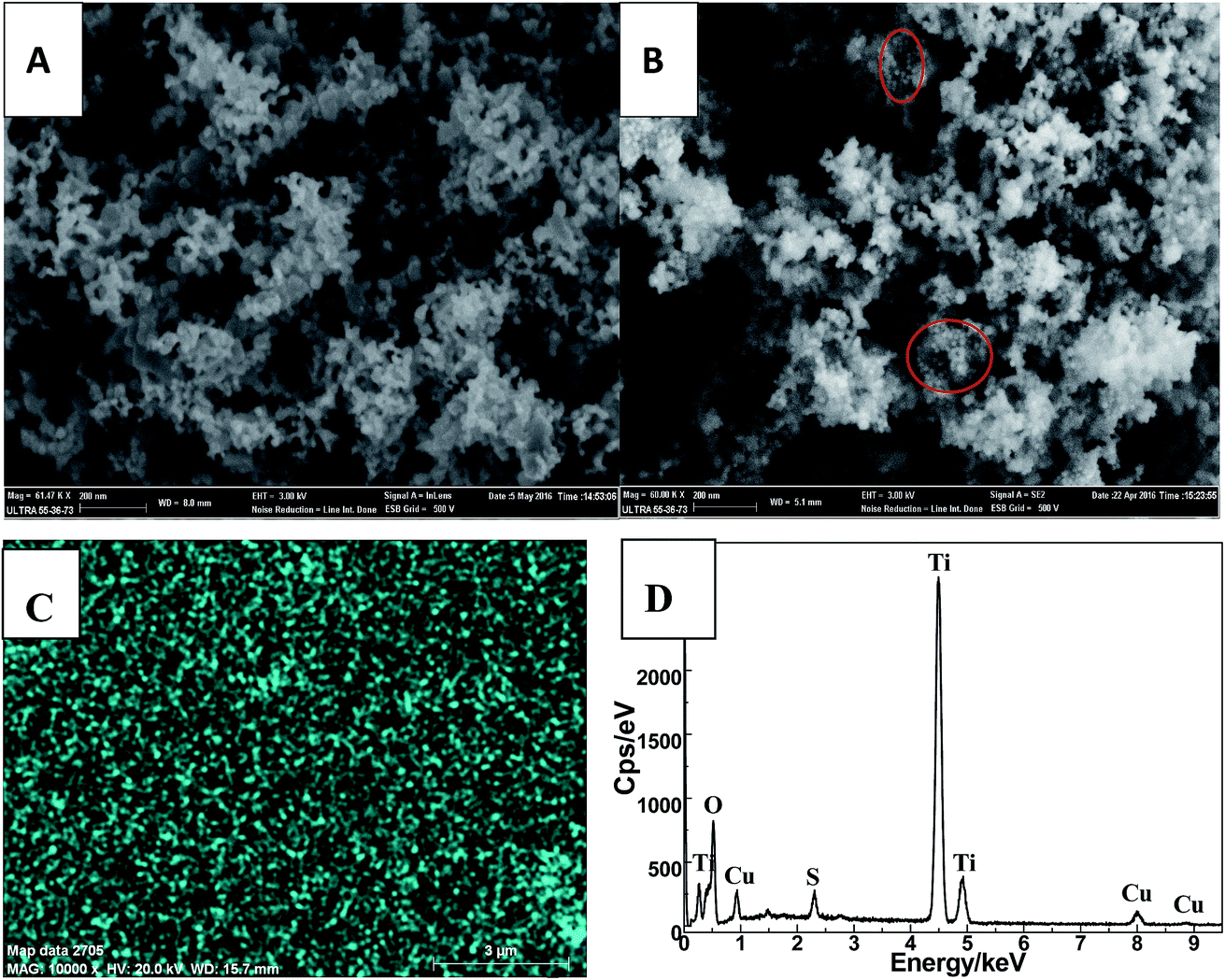
The morphology of as-prepared Cu2S and Cu2S/P25 composites were investigated by FE-SEM, EDS spectrum and high magnification TEM. Fig. 1A and B comparatively shows the FE-SEM of P25 and Cu2S/P25 composites respectively. Fig. 1A shows the typical P25 morphology, the uniform particles spread over the picture. Fig. 1B shows the entry S5 morphology of Cu2S/P25, with the help of P25 image we could see that there are many tiny nanoparticles anchored over the surface of P25. Red circled area shows that the nanoparticles are uniformly in size and could be assigned to the Cu2S nanocrystals, the particle size of Cu2S is around 15 nm. To clearer present the location of Cu2S nanocrystals, SEM-EDS mapping were applied and the images were shown in Fig. 1C and D. Fig. 1C indicated that the element Cu were not confined in a specific space; they were evenly distributed throughout the entire matrix. The EDS profile shows correct stoichiometry of Cu2S to TiO2 in the nanocomposite structure. The atomic ratio of Cu and Ti in the nanocomposite structure was 3.0 at%![[thin space (1/6-em)]](https://www.rsc.org/images/entities/char_2009.gif) :33.5 at% obtained from the SEM-EDS spectrum as shown in Fig. 1D.
:33.5 at% obtained from the SEM-EDS spectrum as shown in Fig. 1D.
 | ||
| Fig. 1 FE-SEM images of the P25 (A), Cu2S/P25 (B). SEM-EDS mapping of Cu (C) and SEM-EDS spectrum (D) of Cu2S/P25. | ||
Quantum confinement of carriers and enhanced surface effects at nanodimensions are well known to result in large modifications in the structural, optical, and electronic properties of nanoparticles.38,39 Balamurugan B. has reported the size-dependent changes in Cu2O nanoparticles, result in conductivity type inversion on reduction of nanoparticle size.40–42 So it is necessarily to know how and what is the extent the quantum confinement of Cu2S effect on the visible light catalytic performance. In the present work, a series of different Cu2S size were achieved in entry S5 to S7 by controlling the volume ratio of dodecanethiol to 1-octadecene. Fig. 2A–C shows the TEM of Cu2S nanocrystals corresponding to the volume ratio of dodecanethiol to 1-octadecene 1:1, 1:5 and 1:39, respectively, as is shown in Table 1 sample entry S5, S6 and S7. All the Cu2S nanocrystals are uniformly formed and the average diameter is 15 nm, 8 nm and 4 nm respectively. It shows that, with the relative content of dodecanethiol to 1-octadecene decrease, the diameter of Cu2S decrease from 15 nm to 4 nm. The final size is almost one quarter of the original. This provide us perfect opportunities for the investigation the size effect on all kind of properties vary from light absorption to photocatalytic performance.
 | ||
| Fig. 2 The morphology of Cu2S and Cu2S/P25. TEM images of Cu2S nanocrystals synthesized at the temperature of 220 °C with 1 mmol Cu(Ac)2·H2O and (A) 15 ml dodecanethiol and 15 mL 1-octadecene, (B) 5 ml dodecanethiol and 20 mL 1-octadecene, (C) 0.75 ml dodecanethiol and 29.25 mL 1-octadecene. HRTEM image of the Cu2S/P25 heterostructures (D, E). | ||
The TEM image in Fig. 2D shows the unique Cu2S/P25 composites prepared following the entry S5, confirming that the Cu2S nanocrystals distributed uniformly on the P25 nanoparticles. The Cu2S crystals are uniformly in spherical shape and their diameter are 15 nm while the P25 particles are in irregular shape with their diameter approximately of 21 nm. The HRTEM image in Fig. 2E show well resolved {011} lattice fringes (interplanar distance d = 0.84 nm) of Cu2S chalcocite-M crystalline structure (JCPDS 33-0490). Distance d = 0.24 nm in Fig. 2E is the indication of a highly crystalline TiO2 anatase framework corresponding to the {103} crystal planes (JCPDS 88-0866). These exposed facets are clear indicative of the coexistence of Cu2S and TiO2 components, the overlap part of Cu2S and TiO2 indicating that Cu2S/P25 composites pn hetero junctions were formed.
3.1 Phase composition
XRD was carried out to investigate the crystal identity of Cu2S and the effect of Cu2S on the crystal structure of TiO2. Fig. 3 shows the XRD pattern of Cu2S/P25 p–n heterostructure composite materials and the starting material P25 nanoparticles. The P25 powder contains 20% rutile and 80% anatase. The diffraction peaks at 2θ = 25.3, 37.8, 48.0, 53.1, 55.4, 62.7, 68.8 in P25 corresponds to the (101), (004), (200), (105), (211), (204), and (116) planes of anatase TiO2 (JCPDS no. 84-1286). While the peak at 27.4°, 36.1° and 41.5° are also present, indicating there coexists the rutile phase (JCPDS no. 88-1175). The dashed lines in Fig. 1 indicate the correlation of anatase crystal planes of Cu2S/P25 prepared with different reactant amounts. Clearly, the XRD pattern obtained at different ratio exhibit no difference in XRD pattern with P25. The comparison of XRD pattern of Cu2S, P25 and Cu2S/P25 indicate that the interposition of Cu2S in the P25 has no effect on the crystal structure of P25 powders, the main structure is preserved. | ||
| Fig. 3 XRD pattern of Cu2S nanocrystal, P25 and Cu2S/P25 heterostructures. | ||
XPS studies were conducted over Cu2S/P25 in order to understand the chemical state and chemical environment of the Cu element on P25 (Fig. 4). As shown in Fig. 4a, the wide-scan survey spectra of Cu2S/P25 contain O, Ti, C, Cu and S elements; the emergence of the C element can be attributed to residual carbon from the sample and adventitious hydrocarbon from the XPS instrument itself. The Cu 2p core level spectrum, shown in Fig. 4b, is composed of two peaks at the binding energies of 932.48 eV and 951.88 eV, assigned to Cu (2p3/2) and Cu (2p1/2) respectively, which are in good agreement with the reported values of Cu2S (i.e., the characteristic peaks of Cu 2p3/2 for Cu(0), Cu(I), and Cu(II) are at 932 eV, 932.7 eV, and 933.6 eV, respectively). As is known that Cu(II) have the characteristic shake up peaks of 2p3/2 around 940 eV and 957 eV which have not been detected in our experiment. All in all, no Cu or CuS are presented in our sample. The plausible reason maybe could be found in the experiment treatment. In our reaction system, Cu2S/P25 were prepared under an N2 protection atmosphere at 220 °C with the dodecanethiol as reductant, and the reductant is excessive to ensure the complete reduce of Cu2+. The Ti 2p XPS spectrum is shown in Fig. 4c, which was composed by two peaks, the Ti 2p3/2 located at 458.68 eV and the 2p1/2 located at 464.5 eV, respectively, suggesting the presence of Ti(IV) species. They are in fairly well agreement with the literature data of TiO2. The Ti 2p XPS spectrum (Fig. 4c) indicates the incorporation of Cu+ induces no significant changes of the Ti4+ 2p electron density. Meanwhile, the XPS spectra of O 1s (Fig. 4d) split as two peaks at 529.47 eV and 532.00 eV respectively after the deposition of Cu2S NPs, owing to the generation of surface oxygen vacancies. [ M. Xing, J. Zhang, F. Chen and B. Tian, Chem. Commun., 2011, 47, 4947–4949] The surface oxygen vacancies is expected to prohibit the recombination of electron–hole pairs and enhanced the visible light absorption efficiency. The results of XPS indicate that Cu2S/P25 composites have been formed.
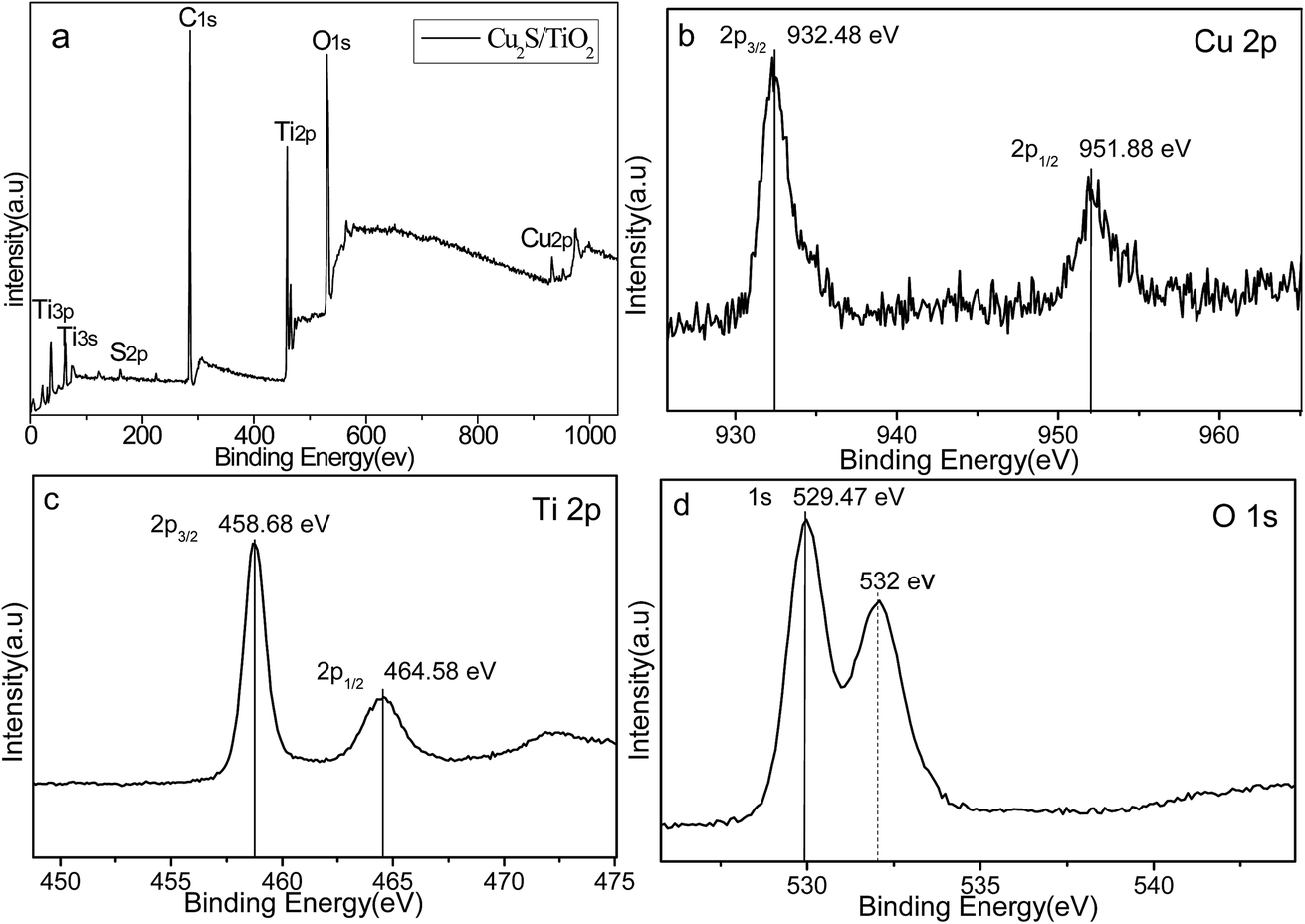 | ||
| Fig. 4 (a) Wide-scan XPS survey spectra for the Cu2S/P25 composites. (b) High-resolution XPS spectrum of (b) Cu 2p, (c) Ti 2p and (d) O 1s for the sample of Cu2S/P25. | ||
Raman spectroscopy is a sensitive tool for investigation the changes on the electrons and molecular structure information. To further identify the doped structure and crystalline of the samples, Raman studies were performed in the range of 120–700 cm−1 that is shown in Fig. 5. All the spectra shown in Fig. 5 share the same Raman peaks at 143, 394, 513, and 636 cm−1, they could be assigned to the Raman-active modes of anatase with symmetries Eg (O–Ti–O symmetric stretching), B1g (O–Ti–O wag), A1g (O–Ti–O symmetric wag), and Eg (O–Ti–O asymmetric stretching), respectively.41 No characteristic Rutile or Brookite phase Raman peaks was found, indicating the composition of pure anatase phase. After doping with Cu2S, the Cu2S/P25 heterostructure shows additional weak peak at 268 cm−1, this could be assigned to the Cu2S characteristic peaks.
 | ||
| Fig. 5 Raman spectra of P25 and Cu2S/P25 with various Cu2S loadings (S1 to S4) and various Cu2S nanocrystal size (S5 to S7). | ||
It is interesting to observe that the Eg peaks are sensitive to the composition change of the Cu2S/P25 hetero structure while the B1g and A1g are inert, the Eg peak at 145.7 cm−1 gradually shifted downward to 142.3 cm−1 as the P25 content increased from S1 to S4, extremely to 136.5 cm−1 for pure P25; however, the Eg peak at 636 cm−1 shifted to the opposite direction. Meanwhile the FWHM narrowed down as the Cu+ disappeared. This indicates that there was an interaction between the Cu and TiO2, S1 contains the highest content of Cu+ and the frequency difference between P25 and Cu2S/P25 also reaches the highest (9.2 cm−1) amongst all the prepared Cu2S/P25 hetero structure. The Cu+ creates crystalline defects in the lattice structure of TiO2 nanocrystals and the defects increase with the increase of Cu content. The crystalline defects affect the characteristic vibrational frequency of the anatase TiO2; it can act as a trap to capture photoelectrons, which makes a contribution to inhibiting the charge recombination. The Eg peaks are also sensitive to the Cu2S particle size change of the Cu2S/P25 hetero structure. As is shown in Fig. 5 S5 to S7, when the particle size of Cu2S increase from 4 nm to 15 nm, the Eg peak at 142.8 cm−1 shift downward to 141.7 cm−1. And again, the Eg peak at 636 cm−1 shift to the upward wavenumber. The smaller Cu2S nanocrystal deposited on Cu2S/P25 hetero structure, the more crystalline defects were created. Thus, the XRD and Raman characterization of TiO2 and Cu2S/P25 demonstrate the high crystallinity of the titania materials and the presence of anatase phase.
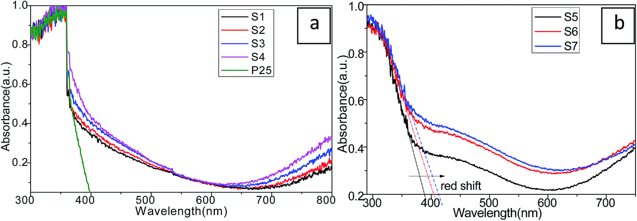
To investigate the optical behavior of the as-prepared Cu2S/P25 and the size effect of Cu2S on the optical property of Cu2S/P25, the UV-vis diffuse reflectance spectra (DRS) were collected and were shown in Fig. 6. Clearly, the largest absorption edge of blank-P25 shown in Fig. 6a was at approximately 370 nm (3.3 eV), whereas the Cu2S/P25 composites show prominence absorption in the visible light region from 400 nm to 800 nm. The absorbance above 400 nm light region was enhanced by the introduction of Cu2S nanocrystals. The composite of Cu2S into the matrix of P25 has a significant effect on the optical property for the Cu2S/P25 composites.
 | ||
| Fig. 6 UV-vis absorption spectra of P25 and Cu2S/P25 with various Cu2S loadings (a) and various Cu2S nanocrystal size (b). | ||
With the increase of Cu2S content (S4 to S1), the absorbance curve becomes relatively flat in the visible light region for Cu2S/P25 while the light absorption feature of Cu2S/P25 nanocomposite in the UV region (particularly at the wavelength of 300 nm) is the same as that of blank-P25. After the addition of Cu2S, the absorption edge is red-shifted to the lower energy value with enhanced absorbance intensity in the whole visible light range. The results of DRS indicate that Cu2S/P25 nanocomposites have the significantly enhanced visible light absorption property and they are able to be “band-gap” photoexcited by visible light irradiation. Electron–hole pairs can be generated by visible light excitation and thus the improved photoexcited performance can be expected.
The Cu2S nanocrystal size effects on the electron excitation transition properties can be referred to Fig. 6b. Fig. 6b S5, S6 and S7, corresponds to the Cu2S nanocrystal size of 15 nm, 8 nm and 4 nm, shows that when the crystal size decrease the absorption edge red shifts to the lower energy and the visible light region absorption enhances accordingly. The smaller, the better visible light absorption efficiency should be expected.
3.2 Photocatalytic activity of as-synthesized Cu2S/P25
It is well known that the photocatalysis activity depends on the photo response efficiency, the catalysts crystallinity, and the phase of the materials. In this work, the visible light induced photocatalytic activities of the as-synthesized Cu2S/P25 were evaluated by photocatalytic degradation of MB under visible light irradiation. For comparison, the photocatalytic activity of every sample was tested under identical conditions. Before irradiation, the suspension was stirred in the black box for about 30 min to ensure the equilibrium have been reached for the MB adsorption–desorption process on the catalysts. The final equivalent absorbance concentrations, i.e., the initial photodegradation concentration of MB, were normalized for different samples. As shown in Fig. 7a, The Cu2S/P25 can efficiently photo degrades MB under visible light irradiation, five different catalysts (S1, S2, P25, S3 and S4) showed 60.8%, 65.3%, 69.1%, 71.4% and 80.1% MB decolorization rates (1 − ct/c0), respectively, under xenon lamp illumination after 240 min. The MB self photodegradation was also included in the figure and it reached 28.0% degradation rate in 240 min. | ||
| Fig. 7 Photodegradation of MB over various samples upon visible light irradiation (a). Kinetic linear fitting curves and the apparent rate constant for liquid-phase photocatalytic degradation of MB over different samples under visible light irradiation (b). | ||
On the basis of a simplified Langmuir–Hinshelwood model, the linear relationship of ln(C/C0) versus time (see Fig. 7b) upon visible light irradiation indicates that MB degradation follows pseudo first order kinetics; the apparent rate constant (k) shown in Fig. 7b was calculated from the plot of ln(C/C0) vs. time. The highest apparent rate constant, obtained for S4, is 6.0 × 10⁻³ min−1, which decrease with the increase of relative Cu2S content in the Cu2S/P25 nanocomposite. The high efficiency performance could be ascribed to its unique cooperative effects and low band gap energy. The photocatalytic activity is in agreement with the rule of visible light region absorption. Generally, the photocatalytic activity is proportional to (Iαϕ)n (n = 1 for low light intensity and n = 1/2 for high light intensity), where Iα is the photo numbers absorbed by photocatalyst per second and ϕ is the efficiency of the band gap transition. The enhancement of the photo activity with Cu2S doping can be partly explained in terms of an increase in Iαϕ resulting from intensive absorbance in the visible region. Cu2S doping expands the wavelength response range of P25 into the visible region and increased the number of photo-generated electrons and holes to participate in the photocatalytic reaction.
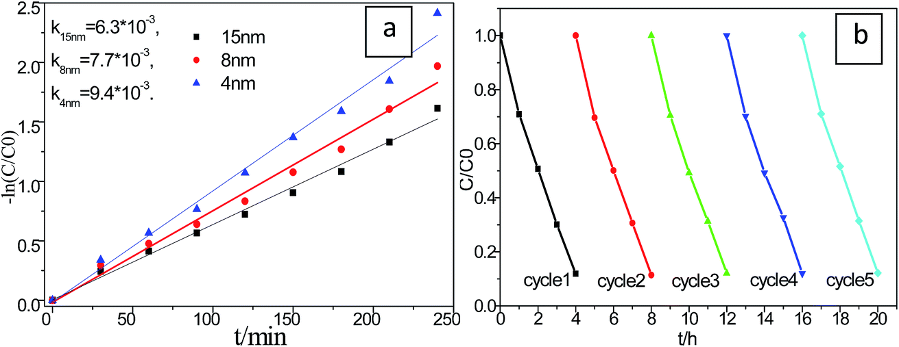
In order to investigate the particle size effect on the photo induced catalytic performance, a series of different Cu2S size were achieved precipitated on P25. As shown in Fig. 8a, the photocatalytic performances of the Cu2S/P25 hetero structures with difference in Cu2S nanocrystal size were tested under visible light irradiation. It is found that their photocatalytic activities are varying with the Cu2S size alternation. The apparent rate constant, obtained for S7 (4 nm), is the highest among them reach to 9.4 × 10⁻³ min−1, which decrease with the increase of Cu2S crystal size in the Cu2S/P25 nanocomposite. Smaller Cu2S crystal size shows the higher photocatalytic activity, which is in agreement with our anticipation from the DRS characterization in Fig. 6b.
 | ||
| Fig. 8 Kinetic linear fitting and the apparent rate constant for photocatalytic degradation of MB over different Cu2S nanocrystal size of Cu2S/P25 hetero structures under visible light irradiation (a). Durability study over Cu2S/P25 hetero structures for MB photodegradation under visible light irradiation (b). | ||
The stability of a photocatalyst is very important for practical applications; thus, a durability test was performed to confirm the stability of the S7 photocatalyst, which achieved the highest performance. According to Fig. 8b, the MB photodegradation efficiency changed very slightly after 5 cycles of the experiment under identical conditions, indicating that the photocatalyst has superior photocatalytic stability.
The Mechanism for the Photocatalytic activity of Cu2S/P25 under visible light excitation could be described as pn heterostructure which is shown in Fig. 9. As is demonstrated from HRTEM and XPS that Cu2S and P25 forms a pn hetero junction and the p-type semiconductor Cu2S acts as the anode (Eg = 1.22 eV), and n-type P25 acts as the cathode (Eg = 3.2 eV). Under visible light irradiation, meso TiO2 exhibited low photocatalytic ability due to its weak absorption “tail”. Once Cu2S are incorporated into P25, the Cu2S/P25 hetero junction catalysts shows enhanced visible region absorption efficiency, upon visible light irradiation the valence band electron resonant with incident photon and excited to conduction band and generate the hot electrons on the Cu2S/P25 surface, significantly increasing the yield of interfacial “hot electrons” with a higher potential energy than P25, and the position of the Fermi level will be shifted closer to the CB of P25. Subsequently, the “hot electrons” transferred to the CB of P25. The pn hetero junction at the interface also helps the transferred “hot” electrons accumulate in the TiO2 CB, preventing them from traveling back to the Cu2S nanocrystals. Since no holes are generated in the valence band (VB) of TiO2, the transferred “hot electrons” in the TiO2 CB should have much longer lifetimes, offering more probability to reduce the O2 adsorbed on the P25 surface and the consequent sequence MB degradation.
 | ||
| Fig. 9 Proposed mechanisms for the photocatalytic activity of Cu2S/P25 under visible light excitation. | ||
4. Conclusions
Cu2S/P25 composites were prepared. SEM shows Cu2S nanoparticles were uniformly formed and distributed on the TiO2 nanoparticles, the average diameter of Cu2S can be tailored from 4 nm to 16 nm and the diameter of P25 was 21 nm. The doping of Cu2S in the P25 shows an enhanced light absorbance in the visible light region. Notably, a lower amount of Cu2S nanocrystals doping on TiO2 nanoparticles exhibited the higher photocatalytic degradation efficiency under visible light irradiation. Size effect shows that the smaller Cu2S crystal size owns the longer absorption wavelength and stronger visible light absorption intensity, and the visible light photodegradation experiment shows the better performance is reached accordingly. The as prepared photocatalysts has superior photocatalytic stability in the degradation of MB experiment.Conflicts of interest
There are no conflicts to declare.Acknowledgements
This work was supported by grants from National Natural Science Foundation of China (No. 21473161 and 21271155), Zhejiang Provincial Natural Science Foundation of China (LZ17B030001), Alexander von Humboldt Foundation (No.1141172) and Zhejiang SCI-TECH University for 521 distinguished scholar's scheme.References
- D. M. Bierman, A. Lenert, W. R. Chan, B. Bhatia, I. Celanovic, M. Soljacic and E. N. Wang, Nat. Energy, 2016, 1, 16068 CrossRef CAS.
- S. F. H. Correia, P. P. Lima, P. S. Andre, R. A. S. Ferreira and L. D. Carlos, Sol. Energy Mater. Sol. Cells, 2015, 138, 51–57 CrossRef CAS.
- P. A. Bharad, K. Sivaranjani and C. S. Gopinath, Nanoscale, 2015, 7, 11206–11215 RSC.
- A. Yella, H.-W. Lee, H. N. Tsao, C. Yi, A. K. Chandiran, M. K. Nazeeruddin, E. W.-G. Diau, C.-Y. Yeh, S. M. Zakeeruddin and M. Graetzel, Science, 2011, 334, 629–634 CrossRef CAS PubMed.
- J. M. Luther, P. K. Jain, T. Ewers and A. P. Alivisatos, Nat. Mater., 2011, 10, 361–366 CrossRef CAS PubMed.
- T. Han, H. Wang and X. Zheng, RSC Adv., 2016, 6, 7829–7837 RSC.
- M. Cheng, G. Zeng, D. Huang, C. Lai, P. Xu, C. Zhang and Y. Liu, Chem. Eng. J., 2016, 284, 582–598 CrossRef CAS.
- S. Esplugas, D. M. Bila, L. G. T. Krause and M. Dezotti, J. Hazard. Mater., 2007, 149, 631–642 CrossRef CAS PubMed.
- J. Schneider, M. Matsuoka, M. Takeuchi, J. Zhang, Y. Horiuchi, M. Anpo and D. W. Bahnemann, Chem. Rev., 2014, 114, 9919–9986 CrossRef CAS PubMed.
- X. Chen, L. Liu, P. Y. Yu and S. S. Mao, Science, 2011, 331, 746–750 CrossRef CAS PubMed.
- A. Fujishima, X. Zhang and D. A. Tryk, Surf. Sci. Rep., 2008, 63, 515–582 CrossRef CAS.
- Z. Zhang, Y. Huang, K. Liu, L. Guo, Q. Yuan and B. Dong, Adv. Mater., 2015, 27, 5906–5914 CrossRef CAS PubMed.
- Y. He, Y. Wang, L. Zhang, B. Teng and M. Fan, Appl. Catal., B, 2015, 168, 1–8 Search PubMed.
- H. Fu, K. Yu, H. Li, J. Li, B. Guo, Y. Tan, C. Song and Z. Zhu, Dalton Trans., 2015, 44, 1664–1672 RSC.
- I. M. A. Mohamed, V.-D. Dao, A. S. Yasin, H. M. Mousa, H. O. Mohamed, H.-S. Choi, M. K. Hassan and N. A. M. Barakat, Chem. Eng. J., 2016, 304, 48–60 CrossRef CAS.
- V. R. de Mendonca, C. J. Dalmaschio, E. R. Leite, M. Niederberger and C. Ribeiro, J. Mater. Chem. A, 2015, 3, 2216–2225 CAS.
- D. Sharma, V. R. Satsangi, R. Shrivastau, U. V. Waghmare and S. Dass, Int. J. Hydrogen Energy, 2016, 41, 18339–18350 CrossRef CAS.
- F. Liao, B. T. W. Lo and E. Tsang, Eur. J. Inorg. Chem., 2016, 1924–1938, DOI:10.1002/ejic.201501213.
- B. M. Rajbongshi, S. K. Samdarshi and B. Boro, J. Mater. Sci.: Mater. Electron., 2015, 26, 377–384 CrossRef CAS.
- K. Shen, K. Wu and D. Wang, Mater. Res. Bull., 2014, 51, 141–144 CrossRef CAS.
- L. Xiao, D. Yuan, P. Li, L. Huang, B.-W. Mao and D. Zhan, Sci. China: Chem., 2015, 58, 1039–1043 CrossRef CAS.
- G. Mondal, P. Bera, A. Santra, S. Jana, T. N. Mandal, A. Mondal, S. Il Seok and P. Bera, New J. Chem., 2014, 38, 4774–4782 RSC.
- J. Li, H. Zhao, X. Chen, H. Jia and Z. Zheng, Mater. Res. Bull., 2013, 48, 2940–2943 CrossRef CAS.
- L. Yang, W. Duan, H. Jiang, S. Luo and Y. Luo, Mater. Res. Bull., 2015, 70, 129–136 CrossRef CAS.
- T. Wang and J. Gong, Angew. Chem., Int. Ed., 2015, 54, 10718–10732 CrossRef CAS PubMed.
- O. E. Rayevska, G. Y. Grodzyuk, V. M. Dzhagan, O. L. Stroyuk, S. Y. Kuchmiy, V. F. Plyusnin, V. P. Grivin and M. Y. Valakh, J. Phys. Chem. C, 2010, 114, 22478–22486 CAS.
- F. Li, T. Han, H. Wang, X. Zheng, J. Wan and B. Ni, J. Mater. Res., 2017, 32, 1563–1572 CrossRef CAS.
- T. Han, D. Zhou and H. Wang, Powder Technol., 2016, 301, 959–965 CrossRef CAS.
- H. Wang, Y. Fu, T. Han, J. Wan and X. Zheng, RSC Adv., 2015, 5, 33570–33578 RSC.
- H. Wang, D. Zhou, Z. Wu, J. Wan, X. Zheng, L. Yu and D. L. Phillips, Mater. Res. Bull., 2014, 57, 311–319 CrossRef CAS.
- H. Wang, D. Zhou, S. Shen, J. Wan, X. Zheng, L. Yu and D. L. Phillips, RSC Adv., 2014, 4, 28978–28986 RSC.
- T. Hanrath, J. Vac. Sci. Technol., A, 2012, 30, 030802 Search PubMed.
- P. V. Kamat, J. Phys. Chem. C, 2008, 112, 18737–18753 CAS.
- H. Eshet, R. Baer, D. Neuhauser and E. Rabani, Nat. Commun., 2016, 7, 13178 CrossRef CAS PubMed.
- S. Akhavan, A. F. Cihan, A. Yeltik, B. Bozok, V. Lesnyak, N. Gaponik, A. Eychmueller and H. V. Demir, Nano Energy, 2016, 26, 324–331 CrossRef CAS.
- M. C. Beard, J. M. Luther, O. E. Semonin and A. J. Nozik, Acc. Chem. Res., 2013, 46, 1252–1260 CrossRef CAS PubMed.
- J. B. Sambur, T. Novet and B. A. Parkinson, Science, 2010, 330, 63–66 CrossRef CAS PubMed.
- D. Debellis, G. Gigli, S. ten Brinck, I. Infante and C. Giansante, Nano Lett., 2017, 17, 1248–1254 CrossRef CAS PubMed.
- A. Sanchez-Soares and J. C. Greer, Nano Lett., 2016, 16, 7639–7644 CrossRef CAS PubMed.
- R. Skomski, B. Balamurugan, P. Manchanda, M. Chipara and D. J. Sellmyer, IEEE Trans. Magn., 2017, 53, 2300307 CrossRef.
- B. Balamurugan and T. Maruyama, J. Appl. Phys., 2007, 102, 034306 CrossRef.
- P. Kumar, A. Kashyap, B. Balamurugan, J. E. Shield, D. J. Sellmyer and R. Skomski, J. Phys.: Condens. Matter, 2014, 26, 064209 CrossRef CAS PubMed.
| This journal is © The Royal Society of Chemistry 2017 |