
 Open Access Article
 This Open Access Article is licensed under a Creative Commons Attribution-Non Commercial 3.0 Unported Licence
UV/ozone-assisted tribochemistry-induced nanofabrication on Si(100) surfaces
Hongbo Wang ,
Bingjun Yu,
Shulan Jiang,
Liang Jiang and
Linmao Qian*
,
Bingjun Yu,
Shulan Jiang,
Liang Jiang and
Linmao Qian*
Tribology Research Institute, State Key Laboratory of Traction Power, Southwest Jiaotong University, Chengdu 610031, Sichuan, China. E-mail: linmao@swjtu.edu.cn; Tel: +86 028 87600687
First published on 14th August 2017
Abstract
A UV/ozone-assisted tribochemistry-induced nanofabrication method is proposed to improve the efficiency of nanofabrication on monocrystalline silicon (Si). Experimental results indicated that the UV/ozone oxidation process provides a simple and efficient method to prepare SiOx films on Si substrates. After UV/ozone oxidation for 10 min, a SiOx film with 3 nm thickness and 42% oxygen content was prepared on a Si substrate. In addition, the SiOx film prepared via UV/ozone oxidation shows super-hydrophilicity, which is beneficial to the following tribochemistry-induced nanofabrication. Through the control of the UV/ozone oxidation period, nanostructures with various depths can be easily fabricated on Si substrates. With the increase of the UV/ozone oxidation period from 0 min to 30 min, the stable depth of the nanogrooves on the Si substrate increased from 2.5 nm to 230 nm. The proposed method provides a new approach for the fabrication of a wide variety of nanoscale structures and devices, including nanogratings, micro/nanofluidic devices, Si molds, and surface textures.
Introduction
As a result of its excellent mechanical and physical properties, monocrystalline silicon (Si) has become the most important semiconductor structural material for electronic and photovoltaic industries.1 The traditional approaches to nanofabrication on Si surfaces include photolithography and nanoimprint lithography, which, to some extent, face technical challenges in resolution, throughput, cost, flexibility, etc.2,3 Therefore, new nanofabrication methods, especially those for Si-based devices, should be thoroughly explored.Recently, tribochemistry-induced nanofabrication has attracted significant attention because of its simplicity, flexibility, and low destruction.3–6 Various patterns can be easily fabricated on Si surfaces via tribochemical scanning and post-etching.7,8 In this method, a silicon oxide (SiOx) etching mask needs to be prepared on a Si surface to resist KOH etching for fabricating nanostructures. The traditional methods for the preparation of SiOx masks, such as thermal oxidation, wet chemical oxidation, and plasma-assisted oxidation, are usually complicated and time consuming. For example, thermal oxidation and plasma oxidation involve five main steps: cleaning in HF solution, aerating gaseous mixture of argon and oxygen, warming sample, treating for several minutes, and annealing. The whole process usually requires more than 40 min.9,10 Simplifying the nanofabrication process and accelerating the preparation of SiOx masks necessitate the development of new preparation methods to further improve tribochemistry-induced nanofabrication.
As a result of its simple, efficient, and green properties, UV/ozone oxidation is widely used to remove hydrocarbons on the surfaces of semiconductors, glasses, ceramics, metals, and other compounds in industrial processes. In addition, hydroxyl-rich oxide films can be generated on Si surfaces during the UV/ozone treatment process,11,12 thus benefitting the tribochemical reaction between SiOx films and SiO2 tips.13 These characteristics indicate that the UV/ozone oxidation approach may be a good candidate method for preparing SiOx films for tribochemistry-induced nanofabrication.
In this study, the UV/ozone oxidation approach was introduced in the preparation of SiOx films for tribochemistry-induced nanofabrication. The effects of UV/ozone oxidation on the oxygen content, thickness, and hydrophilicity of SiOx films were investigated. On the basis of the results obtained with a scanning auger electron spectrometer, the etching-resistant ability of SiOx films was discussed. These findings facilitate the development of the tribochemistry-induced nanofabrication method.
Experimental materials and methods
All the UV/ozone oxidation and nanofabrication experiments were performed on p-type Si(100) wafers with a thickness of 0.5 mm (MEMC Electronic Materials, Inc., USA). Before UV/ozone oxidation, the samples were dipped into 10 wt% HF solution for 2 min to remove the superficial native oxide layer.14,15 After this treatment, every Si surface became H-passivated and showed a water contact angle of about 88°.The whole UV/ozone-assisted tribochemistry-induced nanofabrication process only consisted of three steps, as shown in Fig. 1. First, a SiOx film with a thickness of ∼3 nm was generated on a H-passivated Si(100) surface through a dry oxidation technique with a UV/ozone system (PSDP UV-8T, Novascan, America). During the experiment, the samples were placed 10 mm away from the low-pressure mercury lamps (Fig. 1a). Second, the prepared hydrophilic SiOx film was removed by scanning a SiO2 tip under low load in humid air to expose the target area of the Si(100) substrate (Fig. 1b).16,17 Finally, the exposed Si(100) substrate was selectively etched in KOH solution to form a deep nanogroove (Fig. 1c). As a result of its low etching rate in KOH solution, the SiOx film on the non-scanned area can serve as a mask to protect the Si(100) substrate from etching.18 As this method avoids the complex and time-consuming preparation of masks, the fabrication efficiency can be improved.
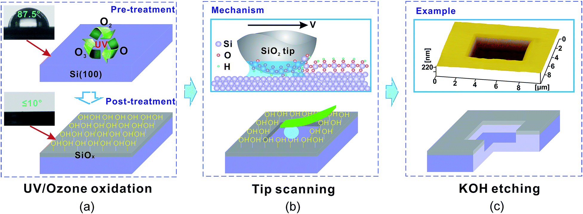 | ||
| Fig. 1 Schematic diagram showing the UV/ozone-assisted tribochemistry-induced nanofabrication process. (a) Growing of SiOx film on H-passivated Si(100) surface via UV/ozone oxidation for 10 min. (b) Scanning a SiO2 tip on a silicon sample in humid air to remove the SiOx mask on the target area. (c) Post-etching of the exposed silicon in KOH solution to fabricate a deep nanogroove. | ||
During the fabrication process, scratching was conducted on a Si substrate covered with SiOx film (SiOx/Si(100)) by using an atomic force microscope (AFM; SPI3800N, Seiko, Tokyo, Japan). The tip was a SiO2 sphere with a nominal radius of 1.5 μm and normal spring constant of 16 N m−1. During the scratching process, temperature was controlled at ∼23 °C, and relative humidity was approximately 45%. In the etching process, a mixture of 20 wt% KOH solution and isopropyl alcohol (volume ratio = 5![[thin space (1/6-em)]](https://www.rsc.org/images/entities/char_2009.gif) :1) was used for selective etching of the exposed Si. The etching temperature was set to 25 ± 1 °C. All the AFM images were scanned in vacuum with silicon nitride tips (MLCT, Veeco Instruments Inc., Plainview, NY, USA) with a spring constant of 0.1 N m−1. The oxygen content and thickness of the SiOx film on the Si substrate were characterized with a scanning auger electron spectrometer (PHI700Xi, ULVAC-PHI, Japan). The contact angle of the surface was tested with an optical contact angle measuring device (DSA-100, KIUSS, Hamburg, Germany).
:1) was used for selective etching of the exposed Si. The etching temperature was set to 25 ± 1 °C. All the AFM images were scanned in vacuum with silicon nitride tips (MLCT, Veeco Instruments Inc., Plainview, NY, USA) with a spring constant of 0.1 N m−1. The oxygen content and thickness of the SiOx film on the Si substrate were characterized with a scanning auger electron spectrometer (PHI700Xi, ULVAC-PHI, Japan). The contact angle of the surface was tested with an optical contact angle measuring device (DSA-100, KIUSS, Hamburg, Germany).
Results and discussion
Preparation mechanism of SiOx film in UV/ozone system
The preparation mechanism of SiOx films in the UV/ozone system was investigated. H-passivated Si(100) samples were treated in the UV/ozone system (25 mW cm−2) for different periods and then characterized with the scanning auger electron spectrometer. As shown in Fig. 2, the UV/ozone oxidation period almost has no effect on the thickness of the SiOx film. All SiOx films have a thickness of ∼3 nm. Nevertheless, the oxygen content of the SiOx film increased with the UV/ozone oxidation period and decreased greatly with the depth of the SiOx film. The untreated sample (0 min) showed extremely low oxygen content. After the UV/ozone treatment lasting 3 min, the oxygen content on the Si surface increased quickly from 10% to 30%. Finally, when the UV/ozone oxidation period reached 30 min, the oxygen content further increased to 46%.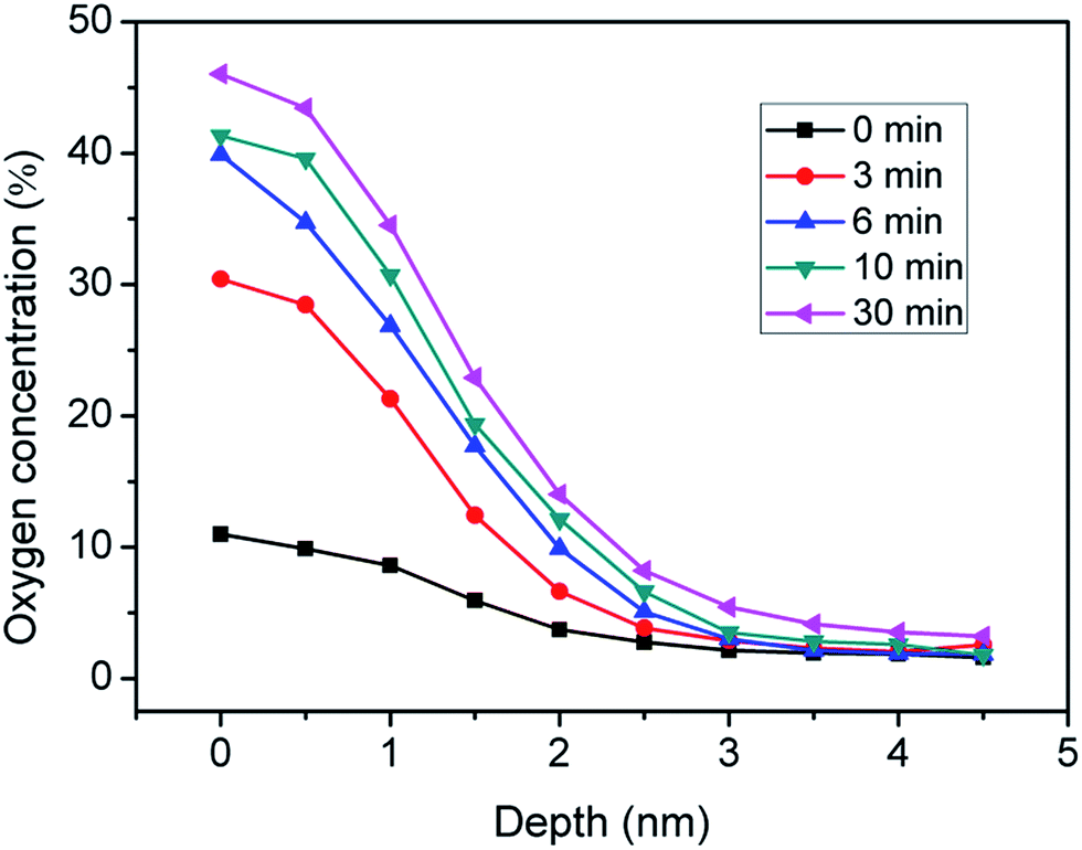 | ||
| Fig. 2 Effect of UV/ozone oxidation period on the oxygen content of SiOx film. | ||
The above results may be attributed to the photo-oxidation reaction on the Si(100) surface in the UV/ozone system.19–21 As shown in Fig. 3, the photo-oxidation reaction mainly included two processes: organic decomposition and oxide densification. The UV/ozone system was equipped with a low-pressure mercury vapor UV lamp with simultaneous emission at 184.9 and 253.7 nm. Hence, ozone and atomic oxygen were continuously generated in the UV/ozone system.19,22 With the help of ozone and atomic oxygen, the surface organic contaminants were decomposed in a short time (Fig. 3a). Thereafter, the exposed Si surface was oxidized by the hydroxyl group and atomic oxygen (Fig. 3b).19,23 Finally, the oxide was gradually densified into a film on the Si(100) surface with the increase of oxygen content, as shown in Fig. 3c.
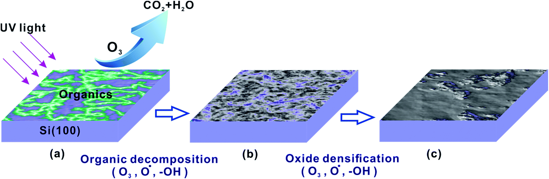 | ||
| Fig. 3 Schematic diagram showing the photo-oxidation reaction process on the Si(100) surface. (a) Original Si(100) substrate covered with organics. (b) Removal of organics by UV/ozone oxidation. (c) Formation of compact SiOx film on Si(100) substrate. | ||
Based on the photo-oxidation mechanism, the thickness of SiOx film was strongly dependent on the wavelength of UV rays.24,25 For the given wavelength of UV rays in our study, the oxidation period almost has no effect on the thickness of SiOx film, but has obvious influence on oxygen concentration, as shown in Fig. 2. With the increase of oxidation period, the atomic oxygens continually diffuse into Si–Si network structure to form Si–O bonds and increase the oxygen concentration of SiOx layers. It is estimated that there are about 3 UV photons crash a Si atom per second in the UV/ozone system. Hence, the Si–Si bonds can be quickly broken by UV photons before 3 min. With continuously proceeding of photo-oxidation process, large quantities of Si–O bonds have been formed in the SiOx layers. As a result, the diffusion of atomic oxygens into the SiOx layers became more and more difficult, which further led to the decrement of growth rate of oxygen concentration.
Clearly, the UV/ozone oxidation process provides a simple and efficient method to prepare SiOx films on Si substrates. Defects and impurities are not observed on the SiOx films. Through the control of the UV/ozone oxidation period, SiOx films with different oxygen contents can be easily obtained (Fig. 2). For comparison purposes, Table 1 is presented to summarize the typical oxidation methods for ultrathin SiOx layers. Dry thermal oxidation is usually performed at high temperatures in a dry oxygen and argon environment. The plasma-assisted oxidation of Si is usually performed with a plasma-enhanced chemical vapor deposition system in a gaseous mixture of nitrogen and oxygen at a low processing temperature. Samples obtained with these two methods require annealing, and the total preparation time is usually more than 40 min. In the wet chemical oxidation process, samples need to be dipped in a diluted HCl solution (1%) or boiled in concentrated HNO3 solution at 80 °C for 20–30 min.10,26,27
| Methods | Preparation process | Preparation time |
|---|---|---|
| Dry thermal oxidation | Cleaning in HF solution | >40 min |
| Aerating argon and oxygen; warming the sample | ||
| Oxidizing for several minutes | ||
| Annealing | ||
| Wet chemical oxidation | Cleaning in HF solution | >30 min |
| Warming the concentrated HNO3 solution | ||
| Oxidizing for 20–30 min | ||
| Plasma-assisted oxidation | Cleaning in HF solution | >40 min |
| Aerating argon and oxygen; warming the sample | ||
| Oxidizing for several minutes | ||
| Annealing | ||
| UV/ozone oxidation | Cleaning in HF solution | <15 min |
| Oxidizing for 10 min |
Effect of UV/ozone oxidation period on the wettability of Si(100) surface
In addition to the mask ability of SiOx films, the wettability of Si(100) substrates can be improved via UV/ozone oxidation. As shown in Fig. 4, after the UV/ozone oxidation treatment for 5 min, the hydrophobic Si(100) surface was converted into a hydrophilic surface with a water contact angle of 10° (Fig. 4b). After treatment for 30 min, a super-hydrophilic Si(100) surface was obtained. Such hydrophilic process may be attributed to the hydroxylation of the Si(100) substrate during the photo-oxidation reaction process,28 this process benefits the tribochemical reaction of SiOx films with SiO2 tips.13 In this study, the UV/ozone oxidation technique provided a reliable approach to prepare the hydrophilic SiOx film for tribochemistry-induced nanofabrication.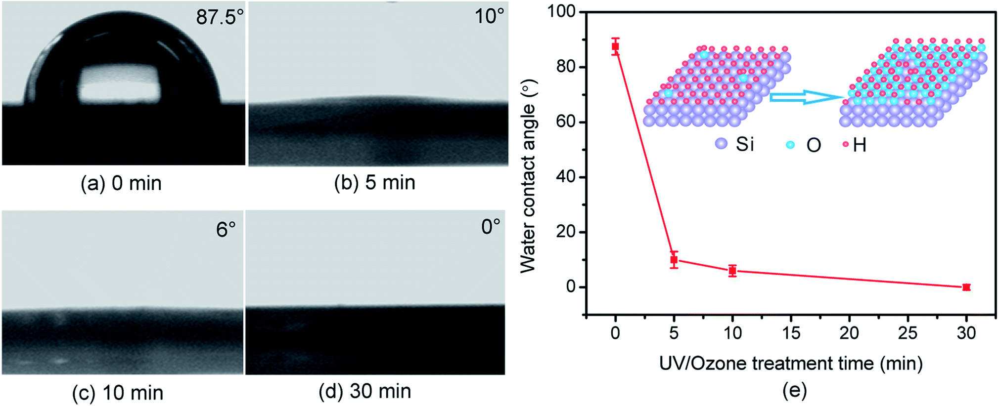 | ||
| Fig. 4 Effect of UV/ozone oxidation period on the wettability of H-passivated Si(100) surface. (a) H-passivated silicon surface. (b–d) UV/ozone-oxidized Si for different periods. (e) Correlation of water contact angle and period of UV/ozone oxidation on the H-passivated silicon surface. | ||
To verify the advantage of UV/ozone oxidation in the tribochemistry-induced nanofabrication, we prepared an ultrathin SiOx film on Si(100) samples via natural oxidation, dry thermal oxidation, and wet chemical oxidation. The thermal oxidation Si(100) sample was prepared at ∼850 °C in a horizontal oxidation furnace for 5 min using a dry thermal oxidation process; the wet oxidation Si(100) sample was prepared in ∼65 wt% HNO3 solution for 30 min at 80 °C.3 In the comparison of the water contact angles of 39°, 36°, and 29° for the SiOx/Si(100) samples prepared via natural oxidation, thermal oxidation, and wet oxidation, the water contact angle of the SiOx/Si(100) sample prepared via UV/ozone oxidation (Fig. 4) emerged as the smallest. As a result of its super-hydrophilic property, the SiOx/Si(100) sample prepared via UV/ozone oxidation showed the largest fabrication depth after scanning a SiO2 tip under the same loading conditions (Fig. 5). After one-cycle scanning, the fabrication depth of UV/ozone oxidation samples is 1.29, 1.56 and 1.66 multiples of natural oxidation, wet-chemical oxidation and thermal oxidation samples, respectively. The increase of the scanning cycles can to some extent increase the increment of fabrication depth. It was noted that even though the UV/ozone oxidation samples are more hydrophilic than the natural oxidation samples, the fabrication depth does not show much advantage under one-cycle scanning. The reason may be attributed to their similar oxygen concentration. Nevertheless, the UV/ozone oxidation can effectively improve the efficiency of tribochemistry-induced nanofabrication.
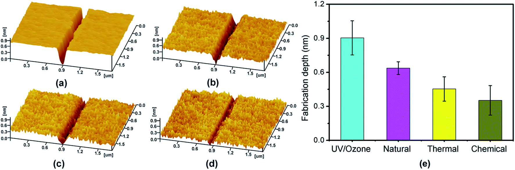 | ||
| Fig. 5 Fabrication depths on Si surface treated with different oxidation methods after one-cycle scanning with SiO2 tip under a normal load of 3 μN. (a) UV/ozone oxidation. (b) Natural oxidation. (c) Thermal oxidation. (d) Wet chemical oxidation. (e) Correlation of fabrication depth and oxidation methods. | ||
Effect of UV/ozone oxidation period on the nanofabrication of Si(100) surfaces
As an improved tribochemistry-induced selective etching approach, the UV/ozone oxidation period has a significant effect on the nanofabrication of monocrystalline Si (Fig. 6). Before fabrication, the superficial native oxide layer on the Si(100) samples was removed in the HF solution and then oxidized in the UV/ozone system for various periods. A target area (5 μm × 5 μm) of these treated samples was scanned by a SiO2 tip under a normal load of 3 μN (the corresponding Hertzian contact pressure was ∼1.137 GPa) in humid air to remove the SiOx film. After scanning the target area for 10 cycles, the fabrication depth was ∼2.5 nm (Fig. 7a).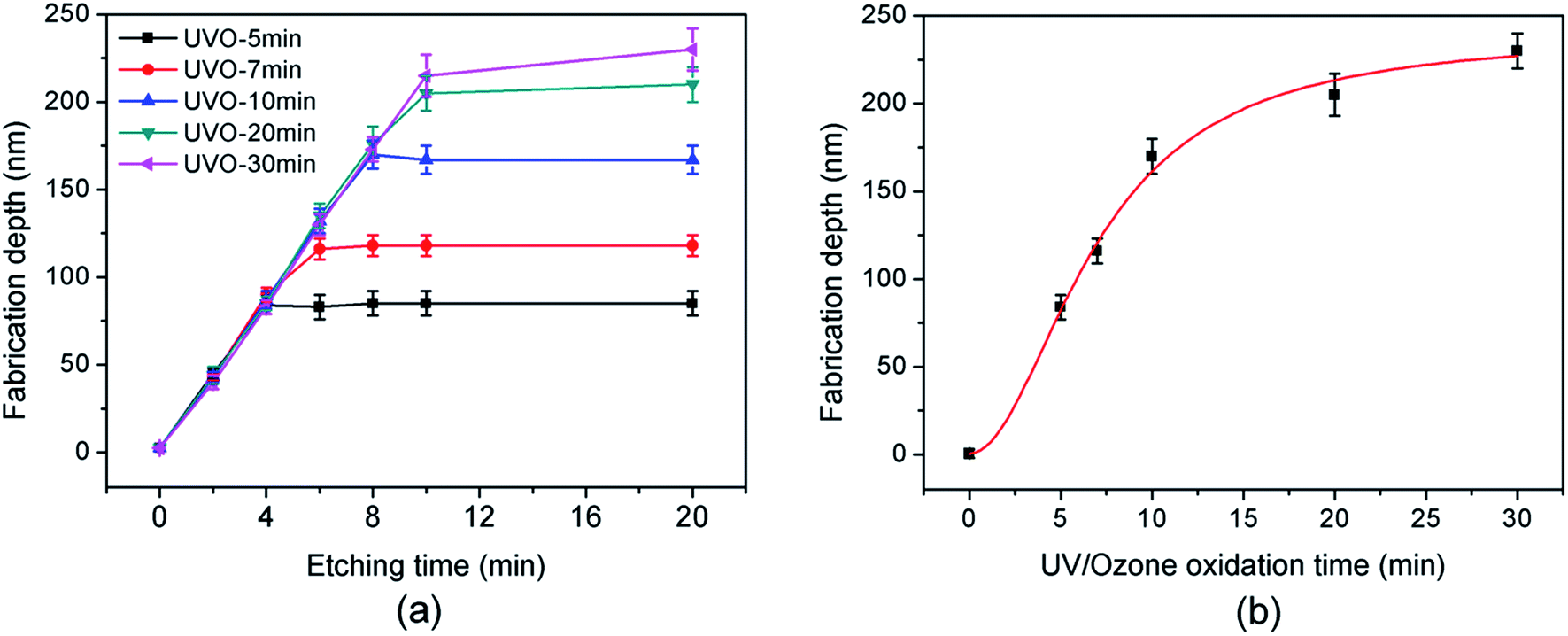 | ||
| Fig. 6 Effect of etching time and UV/ozone oxidation time on the fabrication depth of Si(100) samples. (a) Relationships between fabrication depth, etching time, and UV/ozone oxidation period. (b) Correlation of stable fabrication depth and UV/ozone oxidation period. | ||
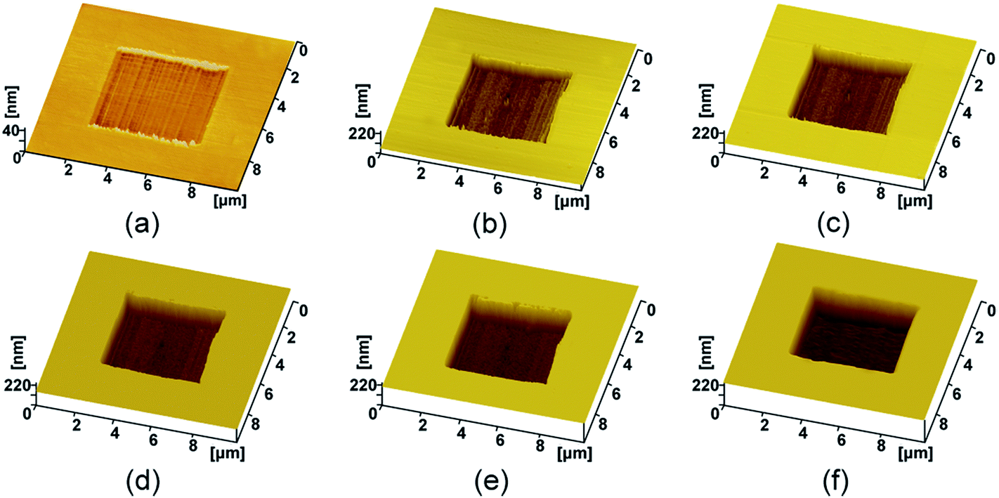 | ||
| Fig. 7 UV/ozone oxidized for different periods Si(100) samples fabricated by tribochemistry-induced selective etching for 20 min. (a) 0 min. (b) 5 min. (c) 7 min. (d) 10 min. (e) 20 min. (f) 30 min. | ||
The corresponding fabrication depths after chemical etching in KOH solution for various periods are shown in Fig. 6a. Fig. 6b plots the variation of the stable fabrication depth of nanogrooves with the UV/ozone oxidation period of Si substrate. Three-dimensional topographies of Si(100) samples oxidized for various periods in the UV/ozone system were characterized by AFM (Fig. 7). The results suggested that the mask ability of the SiOx film prepared on the H-passivated Si(100) surface depended strongly on the UV/ozone oxidation period. With the increase of the UV/ozone oxidation period from 0 min to 30 min, the stable depth of the nanogrooves on the Si substrate increased from 2.5 nm to 230 nm. Therefore, through the control of the UV/ozone oxidation period of the Si(100) samples, nanostructures with various depths were easily fabricated with the improved tribochemistry-induced nanofabrication approach. The SiOx mask on the Si surface was also completely removed after chemical etching in KOH solution for 20 min.
Through the application of the UV/ozone-assisted nanofabrication approach, the efficiency and controllability of tribochemistry-induced nanofabrication can be further improved. Such nanofabrication method provides a new way to fabricate nanoscale structures and devices, including nanogratings, micro/nanofluidic devices, Si molds, and surface textures. The maximum size of the sample is 8 × 8 inch for our UV/ozone system. The fabrication on larger sample is expected to be realized by increasing the number of low pressure quartz mercury.
Conclusions
A UV/ozone-assisted tribochemistry-induced nanofabrication approach was proposed to improve the efficiency of preparing SiOx masks and simplify nanofabrication on monocrystalline Si. The dependence of the oxygen content, thickness, and hydrophilicity of SiOx films on UV/ozone oxidation period was investigated. The etching-resistant ability of SiOx films determined with a scanning auger electron spectrometer was also discussed. The main conclusions can be summarized as follows.(1) During the UV/ozone oxidation process, the SiOx film was quickly prepared on the Si(100) surface through the photo-oxidation reaction. After UV/ozone oxidation for 10 min, a SiOx film with 3 nm thickness and 42% oxygen content was prepared on a Si substrate.
(2) The SiOx film prepared via UV/ozone oxidation showed super-hydrophilicity, which benefitted the following tribochemistry-induced nanofabrication.
(3) Through the control of the UV/ozone oxidation period, nanostructures with various depths were easily fabricated on a Si substrate. With the increase of the UV/ozone oxidation period from 0 min to 30 min, the stable depth of the nanogrooves on the Si substrate increased from 2.5 nm to 230 nm.
Conflicts of interest
There are no conflicts of interest to declare.Acknowledgements
The authors are grateful for the financial support by the National Basic Research Program (No. 973-613323), Natural Science Foundation of China (51527901) and Self-developed Project of State Key Laboratory of Traction Power (2017TPL_Z02).References
- F. Priolo, T. Gregorkiewicz, M. Galli and T. F. Krauss, Nat. Nanotechnol., 2014, 9, 19–32 CrossRef CAS PubMed.
- C. Keimel, S. Y. Chou and J. Gu, Nature, 2002, 417, 835–837 CrossRef PubMed.
- J. Guo, B. J. Yu, L. Chen and L. M. Qian, Sci. Rep., 2015, 5, 16472 CrossRef CAS PubMed.
- C. F. Song, X. Y. Li, H. S. Dong, B. J. Yu, Z. M. Wang and L. M. Qian, Sci. Rep., 2015, 5, 9020 CrossRef PubMed.
- B. J. Yu, H. S. Dong, L. M. Qian, Y. F. Chen, J. X. Yu and Z. R. Zhou, Nanotechnology, 2009, 20(46), 465303 CrossRef PubMed.
- J. W. Park, N. Kawasegi, N. Morita and D. W. Lee, Appl. Phys. Lett., 2004, 85, 1766–1768 CrossRef CAS.
- J. Guo, C. F. Song, X. Y. Li, B. J. Yu, H. S. Dong, L. M. Qian and Z. R. Zhou, Nanoscale Res. Lett., 2012, 7, 152 CrossRef PubMed.
- S. Miyake and J. Kim, Nanotechnology, 2005, 16, 149–157 CrossRef CAS.
- J. C. Tinoco, M. Estrada and G. Romero, Microelectron. Reliab., 2003, 43, 895–903 CrossRef CAS.
- A. H. Azman, R. M. Ayub, M. K. Md Arshad, S. Norhafiezah, M. F. M. Fathil, M. Z. Kamarudin, M. Nurfaiz and U. Hashim, IEEE Int. Conf. Semicond. Electron., 2014, 392–395 Search PubMed.
- N. S. McIntyre, R. D. Davidson, T. L. Walzak, R. Williston, M. Westcott and A. Pekarsky, J. Vac. Sci. Technol., A, 1991, 9, 1355 CAS.
- T. Ito, T. Matumoto and K. Nishioka, Surf. Coat. Technol., 2013, 215, 447–451 CrossRef CAS.
- J. X. Yu, L. M. Qian, B. J. Yu and Z. R. Zhou, J. Appl. Phys., 2010, 108, 034314 CrossRef.
- H. T. Lee, J. S. Oh, S. J. Park, K. H. Park, J. S. Ha, H. J. Yoo and J. Y. Koo, J. Vac. Sci. Technol., A, 1997, 15, 1451–1454 CAS.
- M. Kepenekian, R. Robles, C. Joachim and N. Lorente, Nano Lett., 2013, 13, 1192–1195 CrossRef CAS PubMed.
- K. Mizuhara and S. M. Hsu, Tribology, 1992, 21, 323–328 CAS.
- J. X. Yu, S. H. Kim, B. J. Yu, L. M. Qian and Z. R. Zhou, ACS Appl. Mater. Interfaces, 2012, 4, 1585–1593 CAS.
- J. W. Park, S. S. Lee, B. S. So, Y. H. Jung, N. Kawasegi, N. Morita and D. W. Lee, J. Mater. Process. Technol., 2007, 187–188, 321–325 CrossRef CAS.
- E. Yilgor, O. Kaymakci, M. Isik, S. Bilgin and I. Yilgor, Appl. Surf. Sci., 2012, 258, 4246–4253 CrossRef CAS.
- J. Jeong, K. Sekiguchi, W. Lee and K. Sakamoto, J. Photochem. Photobiol., A, 2005, 169, 279–287 CrossRef CAS.
- J. Zhao and X. Yang, Build. Environ., 2003, 38, 645–654 CrossRef.
- K. Choi, S. Ghosh, J. Lim and C. Lee, Appl. Surf. Sci., 2003, 206, 355–364 CrossRef CAS.
- A. Delman, L. Milton and B. Simms, J. Polym. Sci., Part A-1: Polym. Chem., 1969, 7, 3375–3386 CrossRef CAS.
- H. Oyanagi and A. Fukano, AIP Conf. Proc., 2004, 716, 32–35 CrossRef CAS.
- A. Fukano and H. Oyanagi, J. Appl. Phys., 2003, 94, 3345–3349 CrossRef CAS.
- N. Kherani and Z. Chowdhury, US, US20130298984, 2013.
- B. Stegemann, K. M. Gad, P. Balamou, D. Sixtensson, D. Vössing, M. Kasemann and H. Angermann, Appl. Surf. Sci., 2017, 395, 78–85 CrossRef CAS.
- P. Y. Zhang, F. Y. Liang, G. Yu, Q. Chen and W. P. Zhu, J. Photochem. Photobiol., A, 2003, 156, 189–194 CrossRef CAS.
| This journal is © The Royal Society of Chemistry 2017 |