
 Open Access Article
 This Open Access Article is licensed under a Creative Commons Attribution-Non Commercial 3.0 Unported Licence
Inkjet printed nanomaterial based flexible radio frequency identification (RFID) tag sensors for the internet of nano things
Ravina Singha,
Eric Singh b and
Hari Singh Nalwa*c
b and
Hari Singh Nalwa*c
aHaas School of Business, University of California at Berkeley, Berkeley, California 94720, USA
bDepartment of Computer Science, Stanford University, Stanford, California 94305, USA
cAdvanced Technology Research, 26650 The Old Road, Valencia, California 91381, USA. E-mail: nalwa@mindspring.com
First published on 16th October 2017
Abstract
The Internet of Things (IoT) has limitless possibilities for applications in the entire spectrum of our daily lives, from healthcare to automobiles to public safety. The IoT is expected to grow into a trillion dollar industry worldwide over the next decade. The components of the IoT will be integrated with cloud computing, which will facilitate easy access and analysis of big data stored in cloud systems across the globe. Radio frequency identification (RFID) technology is based on wireless communication systems and offers easy integration into the Internet cloud system. The potential of RFID tag sensor technologies has been studied in different industrial sectors including healthcare, food safety, environmental pollution, anti-counterfeiting of bank-notes and fake medicines, factories, customer shopping behavior, logistics, public transport, and safety. In this review article, the role of inkjet-printed RFID tag sensors is described in the emerging fields of IoT and the Internet of Nano Things (IoNT). This review is concerned with the use of inkjet-printed nanomaterials to fabricate RFID-enabled devices as a component of IoT technology. Inkjet-printed flexible RFID tag sensors based on nanomaterials including multilayer graphene, carbon nanotubes, gold, silver and copper nanoparticles, conductive polymers and their based composites used for detecting toxic gases and chemicals are discussed. Inkjet-printed nanomaterial-based RFID tag sensors that can be easily printed on flexible paper, plastic, textile, glass, and metallic surfaces, show potential in flexible and wearable electronics technologies. Finally, challenges such as energy and safety issues for RFID tag sensors are analyzed.
Introduction
Inkjet-printing is one of the low-cost techniques for directly printing electronic and optoelectronic materials on large-area surfaces for applications in flexible printed electronics.1 Different types of conductive materials including silver, copper, conducting polymers, carbon nanotubes, and graphene oxide have been used in developing nanoparticle and organometallic inks for fabricating thin-film transistors (TFTs), solar cells, light-emitting devices (LEDs), display devices, tissue engineering materials, sensors, and radio frequency identification (RFID) tags.2 Reviews describing the applications of RFID technologies, the properties of different inkjet inks, and RFID-enabled communication systems are available in the literature.1,3 Inkjet-printed RFID tags have also attracted much attention from the scientific community for developing wireless sensors as a component of the Internet of Things (IoT) technology.The Internet has changed human life and social interactions by connecting each other by sharing information through a complex communication network. Mobile phones and their easy connectivity to the Internet have become a major force not only in social media but also in developing new technologies. The Internet of Things (IoT) refers to a worldwide interconnected network of functional machines and electronic devices which can interact with each other as well as with human beings.4 The Internet, smartphones, and their connections to billions of things has created the Internet of Things (IoT), which has no limits in connecting objects and exploiting their applications for the social benefits of the worldwide population. The number of connected objects is estimated to grow to 50 billion, while equivalently growing to 1.8 trillion things by 2020 via the Internet according to a reported published by Cisco.5 This growth is a small fraction of connectivity, which means that there are tremendous opportunities of business growth in this area. The McKinsey Global Institute forecasted that the IoT will grow to 11 trillion dollars economy by 2025, including the areas of semiconductor industries, healthcare, supply chains, public transport, and safety.6 The Internet of Things has also created great demand for new technologies such as big data, cloud computing and wireless sensing for future economic growth.
Over the past two decades, tremendous progress for the applications of nanotechnology in electronics, medicine, energy, communication, transportation, agriculture, and food has occurred based on newly developed nanoscale materials and devices.7–19 A significant impact has been seen in the field of nanoelectronics, where faster nanotransistors have been developed for communication technologies.10 In the medical sector, nanomedicine has been used in a range of healthcare industries, including biological imaging, diagnosis tools, and pharmaceutical therapeutic agents for disease prevention and treatments including cancer.18 Furthermore, nanoparticles (NPs) have also played an important role in stem cell research for differentiating stem cells, contrast agent for stem cell imaging, tissue engineering, regenerative medicine, and treatment of various diseases.19 Dressler and Fischer20 described nano-communication as connecting in-body nanoscale communication system with body area networks. Internet-connected devices and communication network will play a major role in the IoT sector in order to access and analyze big data related to a range of nano things. Nanotechnology-based IoT has created a new domain: the Internet of nano things (IoNT).20 The emerging applications of mobile phones via IoT in servicing consumers from healthcare to public transport and the use of nanomaterials-based sensor in flexible wearable electronics will impact both the current semiconductor industry and all other peripheral industrial sectors that are involved in our daily lives; therefore, the integration of nanoscale devices with emerging IoT is imminent.
In this review article, IoT and nanotechnology are briefly introduced in terms of their impact on future technologies. IoNT will be gaining attention in all areas of nanotechnology such as electronics, nanomedicine, energy, agriculture, and health industries. The role of radio-frequency identification (RFID) systems in emerging IoT and IoNT technologies is discussed. The aim of this review is the use of nanomaterial-based ink for developing RFID tag sensors. The inkjet-printed RFID tag sensors based on polypyrrole, graphene, silver, copper and gold NPs, carbon nanotubes (CNTs), and other nanomaterials, which can be easily printed on flexible plastic, textile, paper, glass, and metallic surfaces are summarized. Additionally, the potential of RFID tag sensors in flexible and wearable electronics technologies as well as their challenges, such as health hazard, energy requirements and safety issues, are described.
Radio-frequency identification (RFID) tag sensors
Radio frequency (RF) electronics that uses a passive electromagnetic device and an active electronic transistor to trigger, receive, and process information play an important role in wireless communication systems.21–28 The location markers generally use radio frequency identification (RFID) tag-based sensors. It is the networks of high-performance sensors and actuators connected to the computing systems and the Internet that would facilitate the future developments in the field of IoT and IoNT technologies. RFID technology is a wireless communication method where objects wearing RFID tags (microchips) are identified and tracked utilizing RF waves. RFID system has two basic components: a memory microchip (tag) that store electronic information and an antenna-connected reader network to receive and analyze signals. A wireless sensor is used as well. There are two types of RFID tags: an active RFID tag that requires power to operate and a passive RFID tag that does not requires any power (battery-free) yielding to a longer lifespan. The electromagnetic waves (RF signal) emitted by the RFID reader activate the RFID tag. Joint Information Systems Committee (JISC) Technology and Standards Watch29 classified RFID operating frequencies into 5 different range; low frequency (30–300 kHz), high frequency (3–30 MHz), ultra-high frequency (UHF) (300 MHz to 3 GHz) and microwave frequency (2–30 GHz) corresponding to an approximate reading range of less than 0.5 meter, up to 1.5 meters, up to 100 meters at 433 MHz, and 0.5 to 5 meters between 865–956 MHz, and finally up to 10 meters, respectively. This covers an entire range of electromagnetic spectrum. However, a passive UHF-RFID tag using electric dipole antennas having a 17.5 m tag read range at the 902–928 MHz frequency band has been demonstrated.30 The RFID tags can be attached to objects such as animals or electronic devices for identification and traceability purpose, which give RFID tagging a broad range of applications, including identification of animals and human, passports, use in hospitals, sports, academic and research institutes, tracking items in grocery stores and supermarkets, public transportation and logistics, and other commercial purposes. RFID technology is also a complementary tool to barcodes. However, with a foreseen fast growth in the IoT area, RFID microchip technology is expected to succeed barcode industry in the near future. RFID technology offers several advantages: a passive RFID tag sensor requires no battery, the reading range is up to 10 meters, and the sensors can be manufactured at a low cost.RFID technology will become an integral part of IoT in many industrial sectors, where applications of RFID include healthcare, energy, public transportation and safety, retailing, agriculture, food packaging, construction, and resource management in factories.31,32 RFID tagging is also playing an important role in the supply chain from manufacturers to retailers to consumers to provide real-time information on identification and traceability of different types of products, which improves efficiency and helps increase revenue with IoT.33–37 RFID tags help analyze inventory levels, logistics, and increase product orders in e-grocery supply chain by the IoT applications.38–42 RFID tracks the level of inventory items in real time, enabling flexible warehousing.43–45 Applications of RFID tagging systems have been reported in the fields of railway transport,46 bank note anti-counterfeiting,47 fake medicines,48 food products safety,49,50 customer shopping behavior,51,52 subscriber identity module (SIM) cards,53 counterfeit wines and wine fraud,54 cultural heritage protection,55 tracking the behavior and habitat of fish in deep waters,56 gesture detection,57 agriculture,58 and hospitals for healthcare.59–65 The use of RFID technology in the healthcare industry is rapidly growing and is being used for real-time tracking of patients, improving their safety, and in management and medical supplies in hospitals.66–73 RFID tag-based food poisoning prevention sensors could save human life and reduce medical costs worldwide that occur due to food poisoning borne human fatalities and related diseases.74 The RFID tagging is also a powerful tool in the field of combinatorial chemistry. Vastl et al.75 used a new approach for chemical library synthesis and screening using silicon micro-transponders (p-chips) to a library of variants of the hemagglutinin (HA) peptide sequence in order to bind with an anti-HA antibody (Fig. 1). A library of 108 hemagglutinin (HA) peptide variants was prepared using a split-and-pool approach, and EC50s for each variant was recorded on p-chips where 80% correlation was observed. Therefore RFID technology can be used in combinatorial synthesis for screening and reading chemical IDs.
 | ||
| Fig. 1 RFID tracking in the synthesis, screening, and reading of chemical IDs for the combinatorial chemistry. [Reprinted with permission from ref. 75 Copyright © American Chemical Society.] | ||
Chipless RFID tags are becoming more popular because they can be inexpensively manufactured due to the elimination of the IC chip component compared with traditional chip-equipped RFID tags. The chipless passive RFID tags can be easily inkjet-printed on a variety of flexible substrates including paper, plastic, metal, and textile surfaces and show stability against oxidative environmental conditions.76–80 The applications of chipless RFID tag have been demonstrated for item tracking,81 humidity sensing,82,83 temperature,84 light,85 pipeline for corrosion,86 and evacuation procedures.87 The battery-free (passive) chipless RFID tag is an ideal candidate for wireless communication technology for commercial applications in emerging IoT industries.3,88 The use of RFID and wireless sensor networks (WSN) in IoT ecosystems enables a wide range of smartphone applications, from farming to delivery of food products to grocery stores, and inventory maintenance to food safety.89–93 RFID tagging is gaining more attention due to the Internet, availability of abundant data worldwide, and the low manufacturing cost of RF chips. RFID technology is gaining further momentum with the emergence of IoT and will create tremendous demand of low-cost tags and sensors for wearable electronics. The IoT has been integrated with cloud computing, which will play a major role in analyzing big data stored in cloud systems.94–102 The schematic of an RFID tag sensor is illustrated in Fig. 2, where the resonant antenna is coated with a thin layer of chemically sensitive thin film and has an IC memory microchip.50 RFID tag sensors will be the integral part of emerging IoT and will have a broad range of applications.
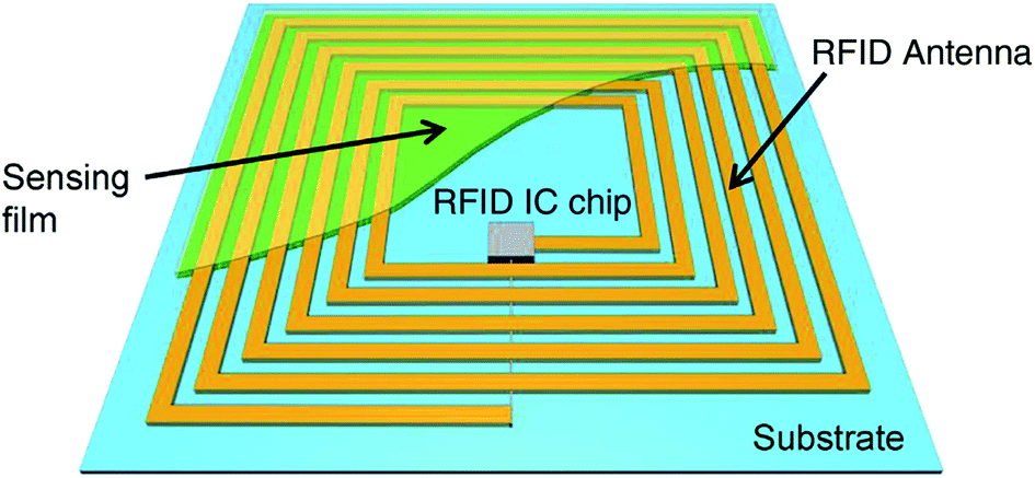 | ||
| Fig. 2 Schematic illustration of a RFID tag sensor. The resonant antenna is coated with a chemically sensitive thin film and has an IC memory chip. [Reprinted with permission from ref. 50 Copyright © Elsevier.] | ||
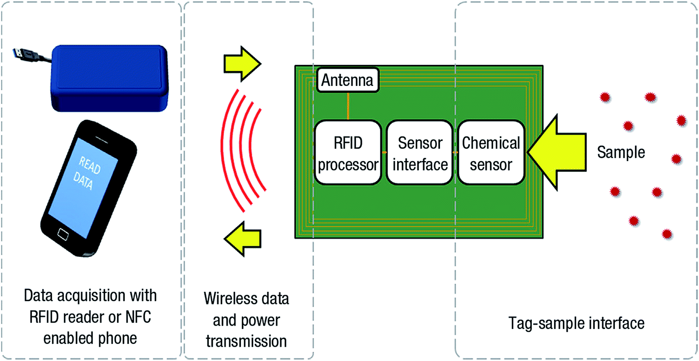
In reference to IoT applications, Kassal et al.103 demonstrated a low-power RFID tag sensor for potentiometric sensitivity. The memory chip in the RFID tag has the capability to measure and eventually store the electrode potential, which is thereafter wirelessly transferred to a smartphone by near field communication (NFC). Fig. 3 shows the RFID/NFC-based chemical tag sensor platform and its operating principle. The RFID/NFC tag chemical sensor is suitable for detecting pH or ion-selective electrodes as part of a chemical sensor networks for IoT. The practical application of RFID/NFC tag sensor was verified for milk spoilage by monitoring the pH value of souring milk over a period of 6 days. The pH of the souring milk decreased to 2.4 for first 2 days due to lactic acid formation. Thereafter the pH value stabilized at 4.3, which was in a good agreement with the 4.28 pH value measured by a laboratory meter. Furthermore, a buffer solution of pH 6.00 was monitored for 5 days where RFID tag recorded data at an interval of every 10 min and transferred the data to the PC. The measurements showed the fluctuation of pH value between 5.89 and 6.10 over the 5 days, averaged to a pH of 6.03. Therefore, RFID/NFC tag sensors show potential for IoT applications.
 | ||
| Fig. 3 Schematic illustration of an RFID-based tag chemical sensor platform and its operating principle. [Reprinted with permission from ref. 103. Copyright © Elsevier.] | ||
Inkjet-printed nanomaterials for flexible electronics
Wearable technologies have created a great demand for the inkjet printing process to fabricate flexible electronic devices such as organic thin film transistors, light-emitting diodes (LEDs), displays, solar cells, supercapacitors, photodetectors, sensors, and RFID tags on a large scale at low cost.2,104 The inkjet printing process is simple, and it is cost-effective to print large-area electronic and optoelectronic devices on a variety of rigid and flexible substrates including metals, ceramics, semiconductor wafers, glasses, polymers, paper, cotton, and synthetic textiles.1,3,104 The flexible plastic substrates of poly(ethylene terephthalate) (PET), poly(dimethylsiloxane) (PDMS), poly(methylmethacrylate) (PMMA), and polyimide (PI) have been widely used for developing flexible and stretchable electronic devices. The well-defined, high-resolution and conductive patterns can easily be fabricated with inkjet printing on different flexible and stretchable substrates for wearable electronics. Selective examples of inkjet printing technology are provided here. A typical inkjet printing process on a substrate is shown in Fig. 4(a) where photonic crystal patterned lines were inkjet printed in a very well-defined closed-packed assembly of NPs.105 Metal-based inkjet printing can provide high-quality conductive patterning on a variety of substrates usable for electronic applications such as RFID antennas, thin film transistors (TFTs), LEDs, display devices and solar cells. Dzik et al.106 used inkjet printing of titania–silica hybrid coatings to develop patterns onto glass and flexible PET substrates. The well-defined patterns having a thickness between 40 nm and 400 nm were fabricated by inkjet printing 1 to 10 layers of titania–silica hybrid. The printed patterns showed excellent optical, mechanical, and photocatalytic activities. The interdigitated photoelectrochemical cells were inkjet printed on flexible PET substrates utilizing the titania–silica hybrid photocatalyst. Fig. 4(b)–(d) shows application aspects of inkjet printing for electronics where interdigitated electrode (IDE) devices were inkjet printed using titania, titania–silica hybrid, and silver NP-based inks. Dzik et al.107 also developed interdigitated photoelectrochemical cells by inkjet printing using a titanium propoxide sol–gel, which was transformed into TiO2 after annealing. The flexible and transparent micro-supercapacitors were developed using graphene-flake ink for printing interdigitated electrodes that exhibited the capacitances of 16 μF cm−2 and 99 μF cm−2 at 90% and 71% transmittance, respectively.108 The graphene-ink-based IDE devices were flexible and showed negligible degradation during mechanical bending. Different types of photonic crystals have been used for inkjet printing to create structural color patterns for applications in security and anticounterfeiting.109–113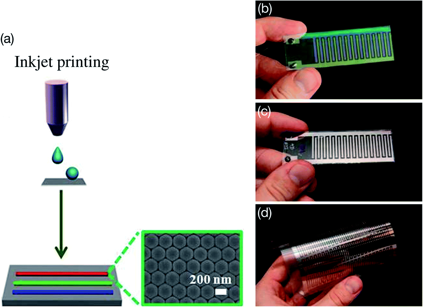 | ||
| Fig. 4 (a) Illustration of inkjet printing on a substrate where the ink droplets' coalescence was controlled. Three red, green, and blue straight photonic crystal (PC) lines indicate good optical properties. Optical microscope images of the inkjet-printed PC patterned lines showing a closed-packed assembly of well-ordered nanoparticles (NPs). The inks contained either poly(styrene-methyl methacrylate-acrylic acid) NPs or silicon dioxide or silver NPs for inkjet printing. [Reprinted with permission from ref. 105 Copyright © American Chemical Society.] The interdigitated electrode (IDE) devices fabricated by inkjet printing on different substrates. (b) Titania electrode inkjet printed over interdigitated ITO layer from sol–gel calcination at 450 °C, (c) titania–silica hybrid sol inkjet printed on Pt electrodes, and (d) 10 × 10 cm prototype IDE device fabricated on a flexible PET substrate using inkjet printing with silver NP-based ink. [Reprinted with permission from ref. 106 Copyright © American Chemical Society.] | ||
The inkjet printing of silver NP ink on flexible substrates has shown great potential for printing conductive patterns for wearable electronic devices. Jiang et al.113 reported printing of silver nanoparticle (AgNP) ink on top of the patterned polymer nanostructures where the polymer nanostructures molded the printed silver and yielding into structural colors. Fig. 5 shows the structural coloration process using molded ink on nanostructured surface (MIONS) technique. The AgNP ink is molded by the underlying prefabricated nanocone arrays on polyethylene terephthalate (PET) substrate.
 | ||
| Fig. 5 (a) Structural coloration process using molded ink on nanostructured surfaces (MIONS) technique. Inkjet-printed silver nanoparticle (AgNP) ink is molded by the underlying polymeric nanostructures of polyethylene terephthalate (PET) substrate. An index-matching lamination process deactivates the unprinted polymeric PET nanostructures exhibiting a transparent background. (b) Schematic illustration of the structural colors observed from the back side of the inkjet-printed silver dot. (c) Color mixing of red, green, and blue pixels. Photographs show printed color bars of red, green, blue, cyan, magenta, and yellow colors with gradient brightness. (d) Cross-sectional SEM image of AgNPs printed onto the PET nanocones. [Reprinted with permission from ref. 113 Copyright © American Chemical Society.] | ||
The silver nanostructure shows different surface profiles; a silver nanocone arrays (NCA) when viewing from the top and a silver nanowell array (NWA) when viewing from the bottom, but both function as 2D gratings in order to diffract light of a particular spectral band. Photographs show the inkjet-printed color bars of red, green, blue, cyan, magenta, and yellow with different brightness, and the SEM image of AgNPs printed onto the PET nanocone arrays. The different colors were tunable by modifying the nanostructured geometries and shapes where a very wide range of colors can be obtained by mixing the red (R), green (G), and blue (B) colors originated from silver dots printed on different geometrical nanostructures. The transparent polyethylene terephthalate (PET) substrate patterned with diffractive geometrical nanostructures was used for printing full color images. The final mixed color is determined by the number of silver dots printed on the each subpixel which is “dots per subpixel” (DPSP). Each subpixel accommodates a maximum of 20 silver dots so the DPSP is 20. This indicates that 21 different brightness levels of colors are controlled using different density of printed silver dots, and therefore 9261 different colors (21 × 21 × 21) can be digitally printed with silver dots on each effective pixel. The MIONS printing allows cost-effective printing of a full-color spectrum of different images. The MIONS can be effectively used for generating plasmonic pixels for security and anticounterfeiting purposes.
The fabrication of electronic devices by the inkjet printing technique is inexpensive compared with existing chemical vapor deposition (CVD), physical vapor deposition (PVD), atomic layer deposition (ALD), lithography, etc. Inkjet inks for conductive metal printing patterns are also obtained from the metal complexes precursor inks after decomposing precursor molecules and undesirable byproducts by sintering at elevated temperatures.114 Sintering plays the most important role for preparing conductive metal printed patterns on different substrates in order to remove unwanted voids, organic solvents, protective surfactants and non-conductive materials without damaging flexible substrates. Kamyshny et al.115 wrote an excellent review on the metal-based inkjet inks applicable for printed electronics and explained inks based on metal nanoparticles (MNPs) and metallo–organic complexes (MC) as well as compared sintering methods such as thermal annealing, photonic sintering under intense light irradiation, plasma sintering, microwave radiation, electrical voltage, and chemical agents triggered sintering in view of their applicability for MNPs and MC-based inks.
Silver conductive inks provide wide examples of both inkjet printed inks based on nanoparticles and molecular precursors which have been widely used in printed electronic circuits for developing different flexible devices including RFID tags. Table 1 lists the electrical resistivities and sintering conditions of silver conductive patterns inkjet printed on different substrates using AgNPs and metal–organic-decomposition (MOD) based inks.116–125 The resistivity remains scattered between 5.8 μΩ cm to 30 μΩ cm between AgNPs and MOD inks which is higher compared with resistivity of bulk silver. Dong et al.121 prepared metal–organic-decomposition (MOD) colorless silver ink by dissolving silver oxalate powder in a mixture of ethyl alcohol, ethylamine, and ethylene glycol after continuously stirring for 30 min at 0 °C. The MOD ink having 27.6% silver contents was used for inkjet printing of silver conductive patterns on flexible PI substrate which showed high reflection with resistivity of 8.6 μΩ cm after curing at 150 °C for 30 min. Shen et al.122 prepared conductive silver paste from silver neodecanoate precursor which was soluble in organic solvents and produced metallic silver after sintering at <200 °C. The paste had 25 wt% silver content and produced silver lines on a substrate by micro-pen direct-writing process. The silver lines showed resistivity of 9 × 10⁻⁶ Ω cm and 5.8 × 10⁻⁶ Ω cm after sintering at 115 °C and 150 °C each for 60 min, respectively. The resistivity of 3 × 10⁻⁶ Ω cm was obtained after sintering 300 °C which was comparable with bulk silver. Sintering of metallic and MOD inkjet inks directly affects their electrical resistivity which has been discussed throughout this article.
| Silver ink | Substrate | Sintering conditions | Resistivity (μΩ cm) | Ref. |
|---|---|---|---|---|
| Bulk Ag | — | — | 1.50–1.60 | |
| Ag nanoplates (119.6 nm) | PI | 100 °C for 15 min | 26.3 | 116 |
| Ag nanoparticles (10–50 nm) | Glass | 260 °C for 3 min | 16 | 117 |
| Ag nanoparticles (21 nm) | PI | 140 °C for 30 min | 30 | 118 |
| Silver hexafluoro-acetylacetonate cyclooctadiene | Glass | 120 °C | 16.8 | 119 |
| Silver citrate | PET | 150 °C for 50 min | 17 | 120 |
| Silver oxalate | PI | 150 °C for 30 min | 8.6 | 121 |
| Silver neodecanoate | Glass | 115 °C for 150 min | 5.8 | 122 |
| AgO2C(CH2OCH2)3H | PET | 130 °C for 30 min | 9.1 | 123 |
| Ag2O/diethanolamine | PET | 75 °C for 20 min | 6.0 | 124 |
| AgNO3/1-dimethylamino-2-propanol | PET | 100 °C for 60 min | 13.7 | 125 |
Inkjet-printed flexible electronic devices have been used in supercapacitors,126 thin-film transistors (TFTs) and inverters,127 differentiation of mesenchymal stem cells,128 mammalian cell structures,129 memory,130 and sensors.131 Inkjet printing will be a low-cost tool for rapid manufacturing of flexible electronic devices.132,133 Various types of conducting inks have been used for the inkjet printing process, including photonic crystals,134 metal NPs,135–142 graphene,143–149 and polymers.150,151 Li et al.127 fabricated metal oxide thin-film transistors (MO-TFTs) by the inkjet printing method without using photolithography. The ITO ink-based TFTs had the shortest channel length of 3.5 μm and showed the mobility of 4.9 cm2 V−1 s−1 and on/off current ratio over 109 indicating inkjet printing will be a cost-effective approach to fabricate short-channel TFTs. Among metal NPs, silver NP ink is more suitable due to its high electrical conductivity than those of copper and aluminum NP inks, because the latter ones, though electrically conductive, tend to easily oxidize. The use of graphene inks has become more popular because of their cost-effective easy processing and coating on large-area flexible devices in addition to their high thermal, chemical, and mechanical stability. RFID-based tag shows promise in flexible electronics from smart-skin to food packaging.152–158
Polypyrrole nanoparticle-based RFID tag sensors
The conjugated polymers such as polythiophene, polypyrrole, polyaniline, poly(p-phenylene vinylene), poly(p-phenylene sulfide), polycarbazole, polyacetylene, polydiacetylene, and their based derivatives show high electrical conductivity upon chemical doping. They have been investigated for many applications including thin-film transistors, solar cells, electroluminescent devices, light-emitting diodes (LEDs), flat-panel displays, photodetectors, and sensors.159 Verma et al.160 fabricated six GHz microstrip patch RFID antennas using two conducting polymers: poly(3,4-ethylenedioxythiophene) PEDOT having a conductivity of 10![[thin space (1/6-em)]](https://www.rsc.org/images/entities/char_2009.gif) 000 S m−1 and polypyrrole (PPy) having a conductivity of 2000 S m−1. Their performance was compared with that of copper patch antenna. The RFID patch antennas showed a maximum gain of 2.2 dB for PEDOT, 3.8 dB for PPy, and 6.0 dB for copper. Verma et al.161 also demonstrated the effect of PPy film thickness on the performance of the microwave antenna. Microstrip antennas were developed on a 3.2 mm thick FR-4 substrate with conducting PPy patches having a conductivity of 2000 S m−1 for operation at 4.5 GHz. The thickness of the PPy antenna patches was less than 168 μm (one skin depth). The 40 μm thick films showed the lowest gain of 2.42 dB and a 38% radiation efficiency while 140 μm thick film exhibited the highest gain of 4.63 dB and a radiation efficiency of 65%. This study supported the fact that the patch thickness influences antenna performance. A microstrip patch antenna was also fabricated using 120 μm-thick PPy film on 3 mm-thick Plexiglas™ substrate, which showed a gain of 5.01 dB at 2.18 GHz compared with a gain of 6.26 dB at 2.2 GHz for a Cu patch antenna under similar conditions.162 Furthermore radiation efficiency of PPy-patch antenna was 60% compared with 80% for Cu-patch antenna. The study indicates the potential of conducting polymer for passive microwave antennas and microwave circuit applications. Chavali et al.163 constructed a wireless UHF-RF-powered sensor operating at 433 MHz for sensing gases and volatile organic vapors. The sensor chip was made of a gas-sensitive composite thin film consisting of PPy and modified multi-walled carbon nanotubes (m-MWCNTs) which were coated on interdigitated gold electrodes. The wireless sensor chip based on PPy/m-MWCNTs composite thin film and RF components detected anesthetic agent, fluoromethyl 2,2,2,-trifluoro-1-(trifluoromethyl) ethyl ether (sevoflurane).
000 S m−1 and polypyrrole (PPy) having a conductivity of 2000 S m−1. Their performance was compared with that of copper patch antenna. The RFID patch antennas showed a maximum gain of 2.2 dB for PEDOT, 3.8 dB for PPy, and 6.0 dB for copper. Verma et al.161 also demonstrated the effect of PPy film thickness on the performance of the microwave antenna. Microstrip antennas were developed on a 3.2 mm thick FR-4 substrate with conducting PPy patches having a conductivity of 2000 S m−1 for operation at 4.5 GHz. The thickness of the PPy antenna patches was less than 168 μm (one skin depth). The 40 μm thick films showed the lowest gain of 2.42 dB and a 38% radiation efficiency while 140 μm thick film exhibited the highest gain of 4.63 dB and a radiation efficiency of 65%. This study supported the fact that the patch thickness influences antenna performance. A microstrip patch antenna was also fabricated using 120 μm-thick PPy film on 3 mm-thick Plexiglas™ substrate, which showed a gain of 5.01 dB at 2.18 GHz compared with a gain of 6.26 dB at 2.2 GHz for a Cu patch antenna under similar conditions.162 Furthermore radiation efficiency of PPy-patch antenna was 60% compared with 80% for Cu-patch antenna. The study indicates the potential of conducting polymer for passive microwave antennas and microwave circuit applications. Chavali et al.163 constructed a wireless UHF-RF-powered sensor operating at 433 MHz for sensing gases and volatile organic vapors. The sensor chip was made of a gas-sensitive composite thin film consisting of PPy and modified multi-walled carbon nanotubes (m-MWCNTs) which were coated on interdigitated gold electrodes. The wireless sensor chip based on PPy/m-MWCNTs composite thin film and RF components detected anesthetic agent, fluoromethyl 2,2,2,-trifluoro-1-(trifluoromethyl) ethyl ether (sevoflurane).
Jun et al.164 developed RFID-based wireless sensor systems using carboxyl (–COOH) group functionalized polypyrrole (C-PPy) spherical NPs having an average diameter of 60 nm. The carboxylated polypyrrole NPs (C-PPy NPs) having different weight ratio of pyrrole monomer (Py) to pyrrole-3-carboxylic acid monomer (C-Py) of 45:1 (C-PPy_1), 30:1 (C-PPy_2), and 15:1 (C-PPy_3) were prepared. The chemical oxidation copolymerization process was used to prepare C-PPy NPs. The C-PPy NPs were characterized by the field-effect scanning electron microscopy (FE-SEM), Fourier-transform infrared (FT-IR) and X-ray photoelectron spectroscopy (XPS). The carboxyl functional groups in the C-PPy NPs provide both stability as well as flexibility after forming a covalent bond on the surface of aluminum (Al) pattern of the RFID antenna. Fig. 6 shows the fabrication process of UHF-RFID sensor tag using C-PPy NPs, photograph and FE-SEM image of the sensing area. The sensor system was fabricated using an RFID reader antenna and a RFID sensor tag coated with C-PPy NPs. A sensor was formed after C-PPy NPs covalently bonded to the passive UHF-RFID tag. Fig. 7 shows the current–voltage (I–V) curves for C-PPy_1 NPs, C-PPy_2 NPs, and C-PPy_3 NPs and the change in the normalized resistance after exposing to different concentrations of ammonia (0.1 ppm to 25 ppm) and acetic acid (1 ppm to 100 ppm) at room temperature. The sensor exhibited a linear behavior between 1 to 100 ppm concentrations of ammonia and acetic acid while a nonlinear sensitivity for less than 0.1 ppm concentrations. The variation in the reflectance properties of C-PPy NPs-based wireless chemical sensors as a function of the concentration of ammonia and acetic acid was also studied. The C-PPY_3-based sensor was able to detect ammonia gas up to a lowest concentration of 0.1 ppm at 900 MHz and acetic acid concentration of 1 ppm at room temperature.
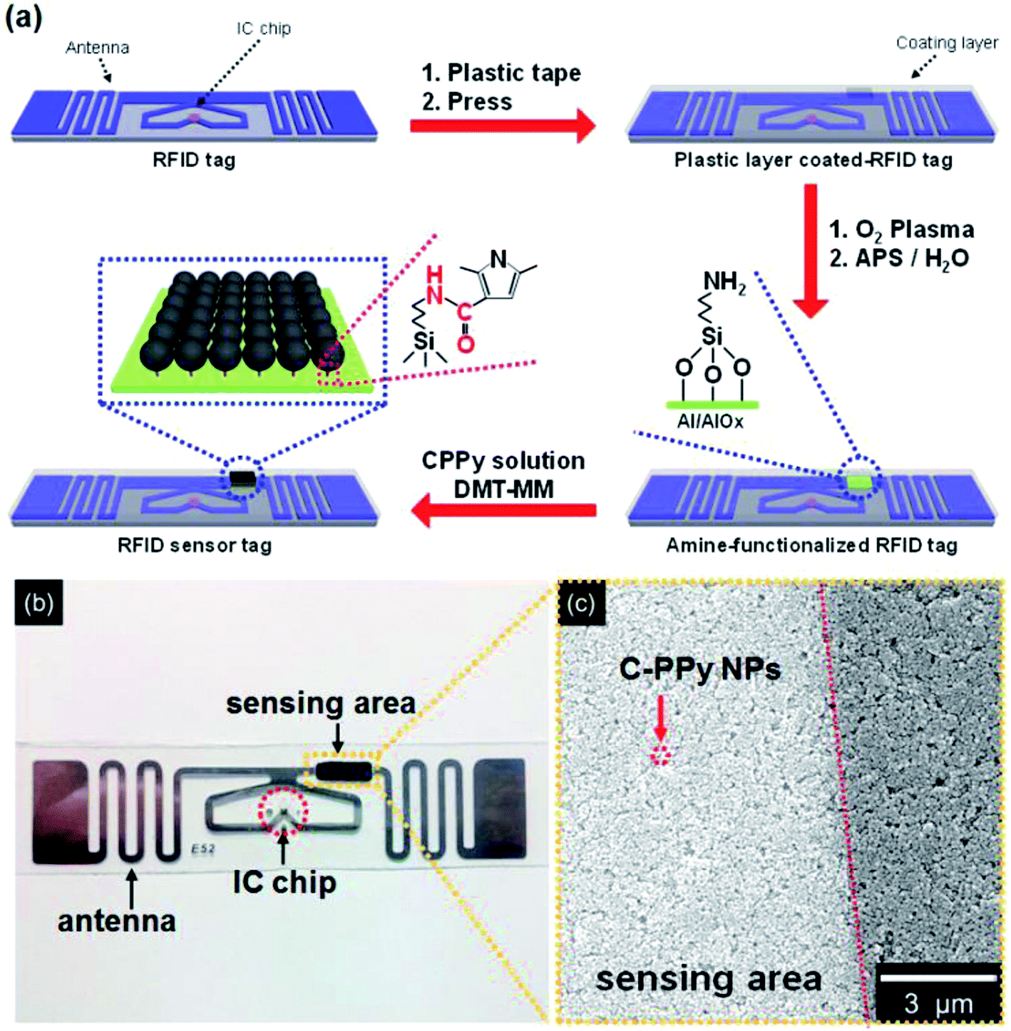 | ||
| Fig. 6 (a) Schematic illustration of the fabrication of UHF-RFID sensor tag using carboxyl group functionalized polypyrrole nanoparticles (C-PPy NPs) where carboxyl functional groups are covalently bonded to the surface of the aluminum tag. (b) Photograph of an UHF RFID-based gas sensor tag. (c) Field-effect scanning electron microscopy (FESEM) image of the C-PPy-NP-immobilized sensing area. [Reprinted with permission from ref. 164 Copyright © American Chemical Society.] | ||
 | ||
| Fig. 7 (a) Current–voltage (I–V) curves for the coated interdigitated array electrode with C-PPy_1 NPs (blue), C-PPy_2 NPs (red), and C-PPy_3 NPs (green), which have different ratios of the carboxyl (COOH) functional groups. The change in the normalized resistance after (b) sequential exposure to varying concentrations of ammonia (0.1 ppm to 25 ppm) and acetic acid (1 ppm to 100 ppm) and (c) periodic exposure to 25 ppm of ammonia gas and 100 ppm acetic acid vapors, and with (d) change in the normalized resistance with a varying range of ammonia and acetic acid concentrations. [Reprinted with permission from ref. 164 Copyright © American Chemical Society.] | ||
The sensitivity of the RFID tag sensor increased from 0.1 ppm for C-PPy_3 NPs to 1 ppm for C-PPy_2 NPs to 5 ppm for C-PPy_1 NPs as the ratio of carboxylic functional group increased. The C-PPy_3 NPs based sensor was exposed to vapors of 14 different volatile organic compounds (VOCs) at 10 ppm fixed concentration. Among acetaldehyde, acetone, butane, benzene, chloroform, methanol, ethanol, hexane, toluene, naphthalene, dimethylamine, trimethylamine and acetic acid, ammonia gas showed the highest sensitivity among all VOCs. The electrical conductivity of the C-PPy NPs was also found to be influenced by the relative humidity (RH) at room temperature when RH increased over 55%. The C-PPy NPs showed a response time of 2 s and recovery time of 55 s. Fig. 8 shows the photographs and reflectance change of the UHF-RFID tag sensor under flat, twisting, and rolling conditions. The sensors retained their flexibility due to the formation of covalent bonding between the carboxyl functional groups of C-PPy NPs and the RFID tag. This was an interesting study because the C-PPy NP-based RFID tag sensors exhibited a wireless operation up to 50 cm and retained sensitivity after repeated bending and twisting, indicating their potential use as flexible gas sensors in wearable electronics.
 | ||
| Fig. 8 Photographs of the C-PPy nanoparticle-based UHF-RFID tag sensor under different deformation conditions: (a) flat, (b) twisting, and (c) rolling. (d) Normalized reflectance change under flat, twisting, and rolling conditions. [Reprinted with permission from ref. 164 Copyright © American Chemical Society.] | ||
Graphene-based RFID tag sensors
With the discovery of graphene, two-dimensional materials such as transition metal dichalcogenides (TMDs) have attracted the attention of the scientific community.165–168 Graphene exhibits unique properties including a high carrier mobility,169 optical transparency,170 mechanical strength,171 and thermal stability,172 which are useful for many different applications including solar cells,173,174 flexible and multifunctional sensors,175,176 and RF electronics.177–183 Huang et al.184 developed an RFID antenna using binder-free graphene laminate. The binder-free graphene ink containing graphene nanoflakes was transformed into a graphene laminate, which showed an electrical conductivity of 4.3 × 10⁴ S m−1 and a sheet resistance of 3.8 Ω sq−1. The conducting graphene laminate was patterned and printed on paper to fabricate a dipole antenna. The graphene laminate antenna exhibited a reflection coefficient (S11) of −11.6 dB at 960 MHz. The reflection measured as a function of frequency showed a −10 dB bandwidth from 0.89 GHz to 1.02 GHz, indicating 90% power was transmitted to the RFID antenna. The graphene laminate antenna showed the realized gain of −0.6 dBi at 962 MHz and over −1 dBi between 930to 990 MHz. The realized gain is an indicator of the antenna performance, which shows the effectiveness of transmitted power. Lamminen et al.185 designed a graphene-flake-based screen-printed dipole antenna operating between 2 and 5 GHz. The graphene-flake-based antenna showed 60% efficiency, a maximum gain of 2.3 dBi at 4.8 GHz and degradation after repeated bending. The graphene-flake-based wideband elliptical dipole antenna can be used for flexible and wearable wireless communication devices. Leng et al.186 used graphene nanoflake ink to screen print an RFID antenna on a paper substrate. The RFID antenna showed a maximum gain of −4 dBi, and −10 dB bandwidth ranges between 984 and 1052 MHz and 32% radiation efficiency.
Lee et al.187 developed an RFID tag sensor using platinum nanoparticle (PtNP)-decorated reduced graphene oxide (rGO) for H2 gas sensing. The wireless sensor consisted of two components, PtNP/rGO hybrid based ultrahigh frequency (UHF) sensor tag and RFID reader antenna connected to a network for analyzing RFID feedback. Fig. 9 shows the schematic diagram of the UHF-RFID-based wireless sensor system having a RFID sensor tag that transfers a signal to the RFID reader antenna (signal receiver) connected to a network analyzer. A schematic illustration of the fabrication process of the PtNP/rGO hybrid-based RFID tag sensor for detecting hydrogen gas, field-effect scanning electron microscopy (FE-SEM) images, and the flexibility of the RFID tag sensor for wearable electronics purposes is shown in Fig. 10. The PtNPs/rGO nanocomposites were spin-coated on the RFID antenna pattern of the UHF (900 MHz) passive RFID tag. The RFID sensor tag can detect H2 gas up to 1 ppm at room temperature. The PtNPs/rGO sensor exhibited a linear range of 1–100 ppm and 15 seconds response time. The PtNPs/rGO sensors showed a nonlinear change in sensitivity at less than 1 ppm concentrations of hydrogen gas. The interdigitated microelectrode array (IDA) based sensors displayed reversible and reproducible sensitivity responses to different concentrations of hydrogen gas. The sensitivity of the RFID-based wireless hydrogen gas sensor increased as the concentration of PtNPs on the rGO surface increased. The interactions between hydrogen molecules and PtNPs dispersed on the rGO surface caused a change in electrical resistivity of the RFID antenna, resulting in a shift in the reflectance of the RFID sensor tag showing detection in the hydrogen gas. The wireless sensor tag also exhibited flexibility and mechanical stability under mechanical bending and twisting deformations.
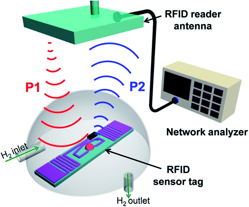 | ||
| Fig. 9 Schematic diagram of the UHF-RFID-based wireless sensor system showing transmission between the RFID sensor tag and RFID reader antenna connected to a network analyzer. [Reprinted with permission from ref. 187 Copyright © American Chemical Society.] | ||
 | ||
| Fig. 10 (a) Fabricating process of PtNPs/rGO hybrid-based flexible RFID sensor tag. Field-effect scanning electron microscopy (FE-SEM) images of the PtNPs/rGO hybrid sensing area at (b) low-, (c) middle-, and (d) high-resolution. (e) Photographs showing flexibility of RFID sensor tag under bending and twisting conditions. [Reprinted with permission from ref. 187 Copyright © American Chemical Society.] | ||
A graphene-based dipole antenna was fabricated on cardboard, usable for the flexible wireless electronics.188 The graphene antenna showed a sheet resistance of 1.9 Ω sq−1 and achieved a length of 143 mm with 40% efficiency and the gain of −2.18 dBi at a frequency of 889 MHz. The graphene dipole antenna-based passive UHF-RFID tag showed a reading range over 5 m at 950 MHz. An RFID tag using a graphene-based dipole antenna and a chip operating in the UHF band was also designed.189 Akbari et al.190 fabricated graphene-nanoplatelet-ink-based passive UHF-RFID tags on a cotton fabric substrate. The performance of the tag was measured after mounting the chips using wireless RFID tag measurements under high-humidity conditions, mechanical bending, and stretching. The tag showed a reading range of 1.6 m that was increased to 3.2 m in 100% humidity, which reversed to normal after drying. The reading range of a bent RFID tag decreased below 1 m while for a flat tag decreased to 1.1 m after 100 bending cycles. The RFID tags were damaged so stretching was not feasible. The low-cost graphene RFID tag can be used as wearable sensors. A wearable RFID device was developed using a flexible antenna by integrating into a facemask and GO-based sensors.191 The GO-based wearable wireless sensor demonstrated the capability of detecting the inhalation/exhalation cycles as well as abnormal patterns of respiration in sleep apnea corresponding to the changes in GO resistance.
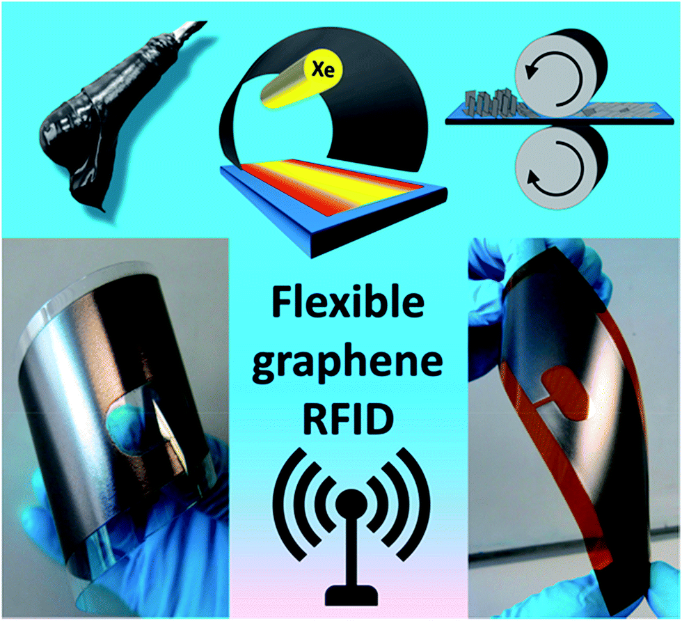
Arapov et al.192 developed graphene-based RFID devices operating at a frequency of 867 MHz on flexible substrates including polyethylene terephthalate (PET), polyimide (PI), and LumiForte paper. The RFID antenna was screen printed from graphene inks followed by photonic annealing and subsequently compressed rolling to decrease the sheet resistance (5 Ω sq−1 or lower) of graphene without any damage to the flexible substrates. Fig. 11 shows screen-printing and post-processing of graphene RFID antennas on two different flexible substrates. Fig. 12 shows the bending performance of graphene-based RFID devices at a 5 mm bending radius, change of resistance up to 1500 bending cycles on PET, PI, and Lumi paper substrates, RFID tag measurements and frequency dependent reading range and printed RFID devices. The graphene/substrate-based composite materials were found to be fatigue resistant exhibiting less than a 1% decrease of electrical conductivity up to 1500 bending cycles and not damaged after 1000 cycles indicating the flexibility and mechanical stability of RFID devices. The photonic annealing of RFID devices showed reading distance range of a transponder as 2.6, 3.1, and 4.0 meters for PET foil, paper, and polyimide after bending, respectively, almost similar to that before bending. The reading range depended upon the sensitivity of microchip and the matching of impedance between the microchip and antenna.
 | ||
| Fig. 11 Screen-printing and post-processing of graphene RFID antennas on flexible substrates including (left bottom) polyethylene terephthalate (PET), (right bottom) polyimide (PI). [Reprinted with permission from ref. 192 Copyright © Wiley.] | ||
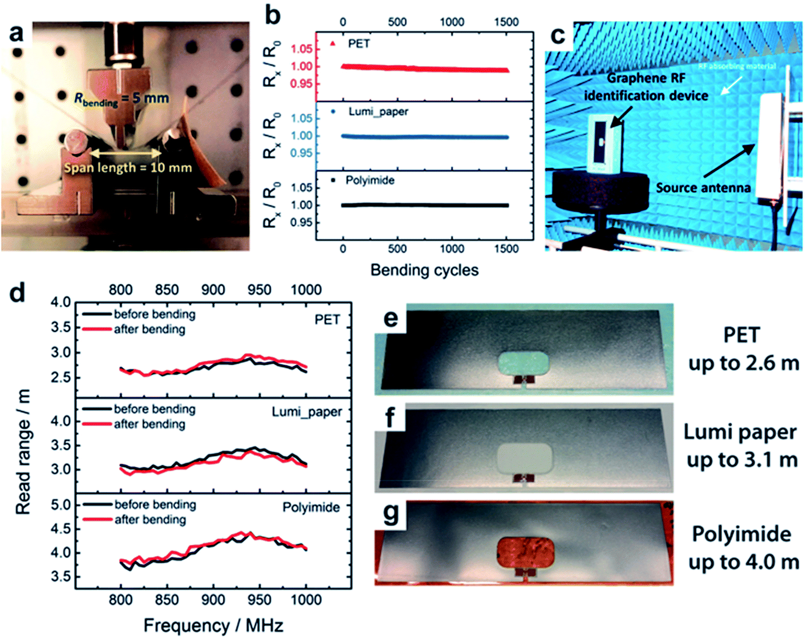 | ||
| Fig. 12 Bending performance of graphene-based RFID devices. (a) Bending setup having 5 mm bending radius, 10 mm span length, and 1 Hz frequency, (b) change of resistance as a function of bending cycles up to 1500 cycles on PET, Lumi paper, and polyimide substrates, (c) graphene RFID tag measurements in an anechoic chamber, (d) frequency-dependent reading range before and after 1000 bending cycles. Photographs of graphene-based RFID devices on (e) PET, (f) Lumi paper, and (g) polyimide substrates at 867 MHz (on the right). [Reprinted with permission from ref. 192 Copyright © Wiley.] | ||
Huang et al.193 reported a chemically sensitive graphene-based modulator having a memory effect for the IoT application. The chemical-gating modulation mechanism based concept was utilized with a graphene field-effect transistor (GFET) device that allows simultaneous multifunctioning including chemical sensing, modulation, and memory functions. This graphene-based sensor does not require a frequency modulation (FM) because the sensor displays wireless radio frequency (RF) signal. Fig. 13 shows the architecture of a network having many sensor nodes using a graphene-based sensing modulator and basic operation concept using the graphene-based sensing modulator. In addition to chemical sensing, the GFET-based nanosensor was also able to detect proteins from milk and Mycobacterium tuberculosis within 2 h of exposure. The single-GFET device operates on a low power of 10 μW making it compatible with Wi-Fi® communication system. In this IoT system, the sensor signal could be received by the smart phones and then analyze with the cloud computing technology. The graphene-based nanosensor modulator uses sensing, RF frequency modulation, and a memory effect. Therefore such GFET-based device can be used for healthcare, chemical sensing, and ubiquitous security systems.
 | ||
| Fig. 13 (a) The nodal architecture of an Internet of nano things using nanomaterial-based sensing modulators. (b) Conceptual illustration of the chemical-sensitive graphene based modulator. [Reprinted with permission from ref. 193 Copyright © Macmillan Publishers Limited/Springer Nature.] | ||
Carbon nanotube-based RFID tag sensors
Carbon nanotubes (CNTs) show interesting electrical, mechanical, thermal, and chemical properties and have been studied for gas and chemical sensing applications.157,194–202 Both single-walled carbon nanotubes (SWCNTs) and multi-walled carbon nanotubes (MWCNTs) have been used for radio frequency applications.203–207 The transparent conductive films of CNTs have been considered as an alternate conductive material to ITO electrodes for flexible electronics. CNTs can be made into conductive inks for inkjet printing purpose. Mustonen et al.208 deposited conductive patterns of carboxyl groups functionalized single-walled carbon nanotubes (SWCNT-COOH) and their composites with poly(3,4-ethylenedioxythiophene)-poly(styrenesulfonate) (PEDOT-PSS) on various substrates using the inkjet printing method. The PEDOT-PSS/SWCNT-COOH composite patterns showed a sheet resistance of 10 kΩ sq−1 and 90% optical transmittance. Lee et al.209 prepared water-based SWCNT inks for inkjet printing. The SWCNT surfaces contained oxygen-containing groups, which increased the dispersion stability, using the UV/ozone treatment. The SWCNTs were concentrated on a circular rim, which was formed by a coffee-ring effect after inkjet printing. The transparent conducting films were printed into 40 layers, which exhibited a sheet resistance of 870 Ω sq−1 with 80% optical transparency at 550 nm wavelength. Shimoni et al.210 reported CNT based transparent conductive arrays inkjet-printed on flexible PET substrate by the coffee-ring effect. Fig. 14 shows the height profile of CNT ring that was inkjet-printed on a heated PET film substrate. The height of the edges was found to be 300 nm around ring while the inside of the ring remained empty. Direct patterning was accomplished by inkjet-printed aqueous dispersion of CNTs, which accumulated on the circular rim after evaporation. The transparent conductive arrays showed a sheet resistance of 156 Ω sq−1 with 81% transparency at a wavelength of 600 nm for the inkjet-printed six layers of CNT rings. This process was used for fabricating CNT-based flexible electroluminescent devices, where inkjet-printed eight-layers of CNT interconnected rings formed the transparent electrodes. These inkjet-printed CNT rings can also be used as transparent conductive electrodes for fabricating flexible solar cells, organic LEDs, flat-panel displays, and touch screens of mobile phones. | ||
| Fig. 14 Height profile of a carbon nanotube ring inkjet-printed on a heated PET film substrate and measured by the (a) mechanical profilometer and (b) optical profilometer. The height of the edges around ring was 300 nm whereas the inside remained empty. [Reprinted with permission from ref. 210 Copyright © The Royal Society of Chemistry.] | ||
Liu and Li211 reported a chipless methane sensor having an ultra-wideband (UWB)-RFID. The proposed sensor head made of palladium (Pd) NP-decorated single-walled carbon nanotubes (Pd-SWCNTs) acts as an electrode. The sensor detected methane as the methane concentration was increased from 0 to 100 ppm and the sensitivity of up to −11.30 dB can be achieved. Fiddes et al. developed wireless sensors with a passive 13.56 MHz RFID tag using carbon black/organic polymer composites. The carbon particles act as the conducting element, whereas the poly(ethylene vinyl acetate) (PEVA), and maleic anhydride (MA) act as a sensing element to identify volatile chemicals212 and biogenic amines in food spoilage.213 Ling et al.214 fabricated a SWCNT-based frequency-modulated RFID wireless tag sensor for detecting ammonia (NH3) gas. The passive wireless sensor tag was made of a SWCNT network-based flexible sensor, RF antenna, and ring oscillator. The large-area SWCNT network increased sensitivity by 0.76% ppm and the sensor exhibited a linear response between the resistance and NH3 concentration. The FM-modulated passive RFID wireless tag sensor is useful for powerless low-level NH3 detection. Bekyarova et al.215 prepared poly(m-aminobenzenesulfonic acid)-functionalized SWCNTs (SWCNT-PABS) for ammonia gas sensing. The resistance increase after exposure ammonia is associated with deprotonation process of the PABS side chain of sulfonic acid groups that induces electron transfer between SWCNT and PABS. Fig. 15 shows the mechanism of interaction between SWCNT and PABS during exposure to HCl and NH3. As the thickness of SWCNT–PABS film is reduced the sensitivity increases. Lee et al.216 developed an RFID tag sensor using SWCNT–PABS films to increase sensitivity toward gaseous molecules. The SWCNT–PABS-based planar sensor was fabricated on a paper substrate for ammonia gas sensing. The PABS-functionalized SWCNTs were integrated into an antenna to develop an antenna-based wireless gas sensor.
 | ||
| Fig. 15 The mechanism of interaction of SWCNT–PABS with HCl and NH3. The arrows point out the charge transfer process between the SWCNT and PABS. [Reprinted with permission from ref. 215 Copyright © American Chemical Society.] | ||
Bhadra et al.217 developed a hydrogel-pH-electrode based on NFC technology for detecting fish spoilage. The sensor showed a detection limit of 1.5 ppm and can identify bacterial population up to 107 cfu g−1 for real-time monitoring of fish spoilage at 24 °C to 4 °C storage conditions. The wireless sensor can be embedded in packaging material for monitoring purposes and requires no integrated circuit. A CNT-based chemiresistor for wireless pH sensing has also been reported.218 Yang et al.219 used inkjet-printed SWCNT composite film on a paper substrate for developing a conformal RFID antenna in a chipless RFID-enabled sensor node for detecting toxic gases. The tag had an extended bandwidth from 810 to 890 MHz, and the impedance performance was measured up to 1 GHz. The 25-layer SWCNT composite film was used for gas detection due to its stable impedance-frequency response and low resistance. The change in electrical conductivity of the SWCNT composite film was observed when exposed to very small quantities of ammonia and nitrogen oxide gases, which were detected by the RFID reader. Asad and Sheikhi220 detected H2S gas up to 100 ppb using a CuO/SWCNT hybrid sensor at room temperature. The chemically sensitive CuO/SWCNT hybrid was coated on the top of a 13.56 MHz RFID tag. The RFID tag sensor showed repeatability and stability over 30 days. Liu and Li221 developed a chipless sensor for wideband (UWB) RFID to detect methane. The sensors had interdigitated electrodes made of Pd NP-decorated SWCNTs. The sensor can cover the entire UWB spectrum except for the band that produces the bandgap. The Pd NP/SWCNT-based sensor was used to detect methane from 0 to 100 ppm at room temperature where the sensitivity was observed at −9.32 dB in terms of the amplitude modulation or at −11.30 dB in terms of the frequency modulation of the bandgap frequency. Kutty et al.222 reported a new architecture of inkjet-printed passive UHF RFID tag sensor for detecting CO2 gas. For introducing a sensing function, the RFID tag was made of AgNPs and CNT inks, which showed a reading range of 4 m at 915 MHz.
Food spoilage is a serious concern in the food industry. Nanomaterial-based biosensors have been developed to detect pathogens and biogenic amines. Chemical sensors made from functionalized CNTs and their composites have been used to detect various types of biogenic amines such as putrescine and cadaverine resulting from the spoilage in fish and other raw meat products.223–226 Tanguy et al.227 developed wireless and battery-free RF biosensor for monitoring of food quality. The antenna of a 13.56 MHz RFID tag was modified with a sensor made of a conductive carbon particle/MWCNT nanofiller and a binding agent functionalized MWCNT and a polymer composite. The sensitivity of RFID tag biosensor was increased due to the binding agent functionalized of MWCNTs. Fig. 16 shows the design of a RFID tag and radical polymerized MWCNTs with maleic anhydride (MA) denoted as g-MWCNTs and its composite formed with poly(ethylene-co-vinyl acetate) PEVA. The RFID tag was exposed to a putrescine solution, and the relative amount of radio waves reflected by RFID tags coated with composites of carbon particles (CPs), MWCNTs, and g-MWCNTs as conductive fillers was measured as a function of time of exposure to 0.25 M putrescine solution. RFID tags with CPs/MA/PEVA, MA/MWCNTs/PEVA, and g-MWCNTs/PEVA displayed a cutoff time of 20, 14, and 10 min, respectively. The smaller cutoff time of 10 min for g-MWCNTs/PEVA nanocomposite indicates a fast response to putrescine vapors. The RFID tag cutoff times were also affected by the different concentration of putrescine. When nanocomposites of g-MWCNTs/PEVA were exposed to 0.5, 0.25, 0.1, and 0.05 M concentration of putrescine, the cutoff time resulted in 4, 10, 20, and 28 min, respectively. This research study showed that RFID tag developed from MWCNTs and g-MWCNTs can be used for faster detection of spoilage in food products.
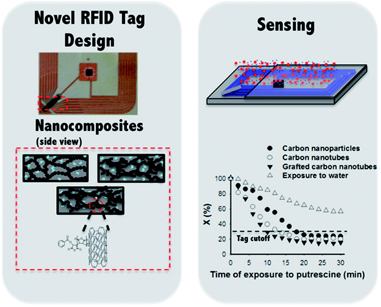 | ||
| Fig. 16 (Left) Illustration of RFID tag design and radical polymerization of maleic anhydride (MA) on MWCNTs and its composite with poly(ethylene-co-vinyl acetate) PEVA. (Right) Schematic illustration of a RFID tag after exposure to a putrescine solution. The relative amount of radio waves reflected by tags coated with composites of carbon particles, MWCNTs, and grafted-MWCNTs as conductive fillers as a function of time of exposure to 0.25 M putrescine. [Reprinted with permission from ref. 227 Copyright © American Chemical Society.] | ||
Silver nanoparticle-based RFID tag sensors
AgNP ink has been commonly used in inkjet printing of wearable electronics due to its low cost, easy preparation process, high-resolution printing, environmental stability, and excellent conductive properties after sintering at elevated temperatures.228–230 Sintering techniques play an important part in preparing silver conductive patterns on flexible substrates for printed electronics. Kell et al.231 reported silver molecular ink formulations for inkjet, screen, and aerosol jet printing. The screen-printed silver traces exhibited a resistivity of 12 μΩ cm after sintering. The aerosol jet ink on glass substrate yielded two times higher resistivity compared with bulk silver and strong adhesion to flexible plastic substrates. Table 2 lists linewidth, sheet resistivity and current carrying capacity (CCC) of the silver molecular ink and silver flake ink printed on Kapton and PET substrates. The silver molecular ink printed patterns on Kapton (polyimide) substrate showed lower sheet resistivity and higher current carrying capacity than those of silver flake ink printed patterns on PET substrate. Fig. 17 shows the topography of thermally and photonically sintered silver molecular ink traces analyzed from optical profilometry which showed almost similar resolution and pitch. The linewidth and line spacing of 105 μm and 45 μm for thermal sintering and 108 μm and 50 μm for photonic sintering, respectively, were measured for silver molecular ink. The inkjet formulation printed TFTs having silver molecular ink printed source and drain electrodes onto single-walled carbon nanotubes (SWCNTs) based channel showed mobility of 25 cm2 V−1 s−1 and on/off current ratio up to 105 after sintering at 230 °C for 30 min.| Silver ink type | Substrate | Trace thickness (μm) | Measured linewidth of trace (μm) | Sheet resistivity (mΩ sq−1) | Current carrying capacity (mA) |
|---|---|---|---|---|---|
| Silver molecular ink | Kapton | 0.6–0.9 | 175 | 3.8 | 226 |
| 295 | 3.7 | 328 | |||
| Silver flake ink | PET | 12–16 | 150 | 17 | 161 |
| 275 | 12 | 225 |
 | ||
| Fig. 17 A comparison of the topography of (a) thermally and (b) photonically sintered silver molecular ink traces analyzed from optical profilometry. [Reprinted with permission from ref. 231 Copyright © American Chemical Society.] | ||
Farraj et al.232 used electron beam sintering method to form highly conductive silver patterns of AgNPs. The AgNPs inkjet printed on polyethylene naphthalate (PEN) substrate were subjected to rapid ebeam irradiation. Fig. 18 shows the photograph of flexible silver printed pattern after ebeam sintering and the effects of conveyor speed and current as a function of energy dose on the resistivity of printed silver patterns at a fixed voltage of 110 kV. At a fixed current of 18 mA, the exposure time increases with decreasing conveyor speed, leading to higher total energy doses. The resistivity of the silver printed patterns decreases with increasing total energy dose. At constant speed of 3 m min−1, the current increase yields a decrease in resistivity. In both cases, the higher energy dose results into lower resistance of the silver film, though the effect of conveyor speed is more prominent in decreasing the resistance compared with current increase. The printed silver patterns prepared after sintering with 600 kGy energy dose exhibited the lowest resistivity of 4.5 μΩ cm, which was 2.8 times that of bulk silver. The 37% higher electrical conductivity of AgNPs was achieved than that of bulk silver under optimal electron beam-sintering conditions. The ebeam sintering helps in removing the organic stabilizer from the AgNPs surface and also binds AgNPs together due to heat-welding. The ebeam technology can be used for large-scale printed electronics for roll-to-roll processing.
 | ||
| Fig. 18 (A) Photograph of silver printed pattern on a flexible PEN substrate after electron beam (ebeam) sintering process. (B) Change of resistivity as a function of energy dose. Effects of conveyor speed at fixed current of 18 mA and current at fixed speed of 3 m min−1 on the resistance of printed silver patterns. The voltage was fixed at 110 kV. [Reprinted with permission from ref. 232 Copyright © The Royal Society of Chemistry.] | ||
AgNP ink was also prepared by simply dispersing the silver nanopowder in water as reported by Shen et al.233 Silver inks were prepared by adding different amounts of silver nanopowder to a mixture of deionized water and ethylene glycol. Ethylene glycol helps in controlling the silver inks' viscosity as well as the surface tension. The poly(acrylic acid) (PAA)-coated AgNPs were prepared to prevent degradation/oxidation and, therefore, to improve long-term stability at room temperature. The viscosity and surface tension of silver inks increase as the contents of AgNPs are increased. The viscosity of AgNP ink increased from 2.51 mPa s for 5 wt% on silver contents to 4.03 mPa s for 25 wt% of the silver contents. Fig. 19 shows the photographs of silver tracks printed on photo-paper with different line-widths, SEM image of cured silver track and the variation of the printed silver pattern's thickness as a function of the printing cycles. The silver tracks were obtained by printing AgNPs ink up to 10 times for line-width ranging from 0 to 1.5 pt and sintering at 50 °C for 15 min. The line-width of 1.0 pt printed silver track was 526.63 μm. The thickness of silver printed patterns increased with increasing number of printing cycles. Fig. 20 shows the particle size distribution of AgNP ink, TEM image of PAA-coated AgNPs and electrical resistivity of AgNPs conductive patterns as a function of printing cycles. The size of AgNPs varies from 20–230 nm but the mean size ranges from 30–50 nm. The TEM image indicates well-dispersed silver nanopowder in water with particle size between 10–100 nm, where the majority of the NPs are over 40 nm. The silver inks were printed on flexible paper and polyethylene terephthalate (PET) substrates with a commercial color printer. The electrical resistivity of AgNP conductive patterns printed on photo-paper decreased with increasing number of printing cycles (N) and temperature. The 2 and 3 printing cycles showed a significant fluctuation in electrical resistivity which decreased from 139.4 μΩ cm to 10.8 μΩ cm as curing temperature was increased from room temperature to 180 °C and 40.1 μΩ cm to 7.7 μΩ cm as the number of printing cycle was increased from 2 to 3. Interestingly, the value of electrical resistivity of the Ag pattern printed 14 times and annealed at room temperature was found to be similar to that of Ag pattern sintered at 50 °C because the morphologies of Ag patterns did not change at these temperatures. The resistivity of printed AgNP patterns decreased from 8.0 μΩ cm to 3.7 μΩ cm as the sintering temperature was increased from room temperature to 180 °C, which was 20% of the bulk silver under ambient conditions. The electrical resistivity of the printed Ag patterns was affected by the number of printing cycles and annealing temperature. The SEM images of printed AgNP patterns showed little change in morphologies for patterns sintered at room temperature (25 °C) and 50 °C. The formation of cracks and voids was observed in printed AgNP patterns after sintering at 80 °C whereas the AgNP patterns became continuous and smooth after sintering at 140 °C due to the disappearance of AgNP boundaries which also resulted into lower resistivity. The poly(acrylic acid)-coated silver NP inks was used for printing flexible LED devices on photo-paper and PET substrates.
 | ||
| Fig. 19 (a) Photographs of silver tracks printed on photo-paper with different line-widths ranging from 0 pt to 1.5 pt. (b) Optical image of silver tracks printed on photo-paper having 1.0 pt (equal to 527 μm) line-width. (c) SEM image of silver track cross-section printed on photo-paper formed after curing at 50 °C for 15 min. (d) Thickness variation of the printed silver patterns with the increasing number of printing cycles. [Reprinted with permission from ref. 233 Copyright © The Royal Society of Chemistry.] | ||
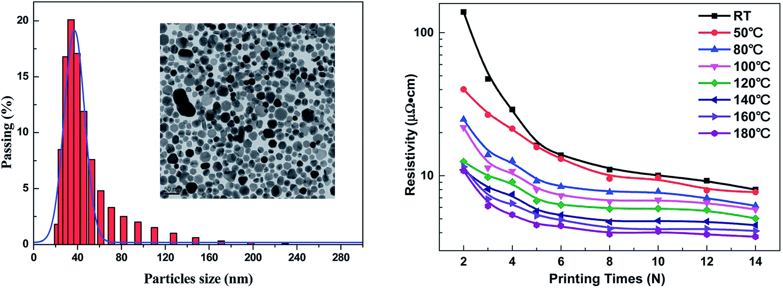 | ||
| Fig. 20 (Left) Particle size distribution of silver nanoparticle (AgNP) ink with an average AgNP size of 30–50 nm. Insert shows the TEM image of AgNPs imparted in the silver ink formulation. (Right) Electrical resistivity of AgNPs conductive patterns printed on photo-paper as a function of the number of printing cycles (N) after heating from room temperature to 180 °C. [Reprinted with permission from ref. 233 Copyright © The Royal Society of Chemistry.] | ||
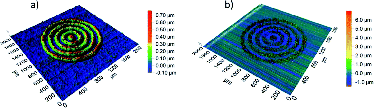
In another study, Wang et al.234 prepared AgNP ink containing up to 80 wt% of AgNPs and obtained high-quality silver nanowires by optimizing the sintering temperature, time, and pressure. Fig. 21 shows a photograph of the written AgNP conductive tacks on a paper substrate bending outward by 90°. The electrical resistivity of AgNP conductive tracks printed on paper substrate was 3.92 × 10⁻⁸ Ωm after sintering for 20 min at 120 °C at 25 MPa pressure. The AgNP conductive patterns written on paper showed an excellent mechanical flexibility because the resistivity increased from 4.01 × 10⁻⁸ Ωm to 5.08 × 10⁻⁸ Ωm after 1000 bending cycles. A flexible LED device was fabricated using these outstanding electrical and mechanical properties of AgNP ink. This study showed that AgNP ink with 80 wt% loading can be used for directly writing flexible electronics on different substrates. AgNP inks have shown excellent potential for inkjet-printed flexible and wearable electronics including RFID tag antennas.235,236
 | ||
| Fig. 21 Photograph of the written pattern using AgNP conductive ink on a paper substrate bending outward by 90°, which was sintered for 15 min at 120 °C and at a pressure of 25 MPa. This indicates good mechanical flexibility of printed patterns using AgNP inks. [Reprinted with permission from ref. 234 Copyright © Nature Publishing Group.] | ||
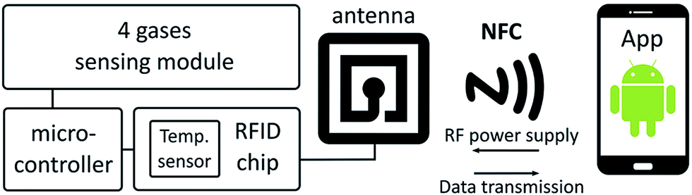
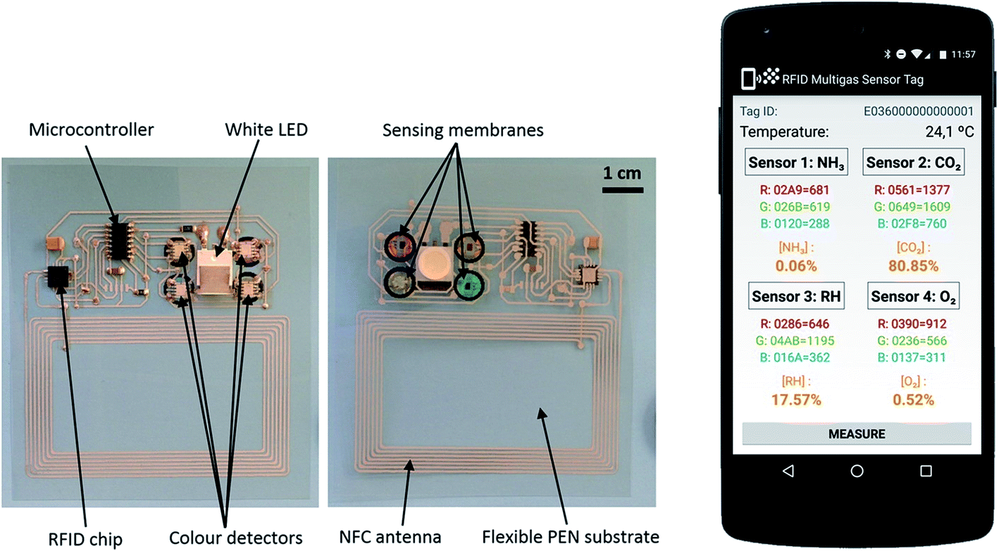
RFID/NFC technology is becoming important for the transmission of data and sensor technology.237–240 Escobedo et al.241 fabricated a passive RFID sensing tag for detecting carbon dioxide, oxygen, ammonia, and relative humidity (RH), which were readable by a smartphone. The tag functions were based on NFC technology to harvest energy and for easy data transfer to a smartphone. In this RFID system, the use of NFC-enabled smartphones is the reader, which eliminates the requirement of an RFID reader. The gas sensor requires very low power to read an optical response using high-resolution digital color detectors. The Android™ operating system was applied for the power supplying and for receiving data from the tag. Fig. 22 shows a block diagram of a multigas-sensing RFID tag sensor where RFID chip is connected to an antenna and data is transmitted to a smartphone. Fig. 23 shows the photographs of both sides of the passive multigas RFID tag sensor and a smartphone using the Android application. The RFID tag was inkjet printed on a flexible poly(ethylene naphthalate) (PEN) film using AgNP-based conductive ink. A digital color detector is located on the flexible PEN surface-facing sensing membranes for reading the optical response from a multigas sensor. A white LED was placed in the center of four sensing membranes to excite the sensors. The optical sensitivity of four membranes was detected by the color detector where oxygen gas has a luminescent response while all remaining three gases have a colorimetric response. The AgNP ink/PEN flexible film-based NFC/RFID tag sensor showed the limit of detection (LOD) as 1.3 × 10⁻³% for O2 gas, 7.9 × 10⁻⁴% for NH3 (gas concentration of 1.5 × 10⁻²%), 0.23% for 5% concentration of CO2 gas, and 1.8% for 15% humidity for a required frequency of 13.56 MHz, which was within the ISO 15693 protocol specification for wireless operation. The response time to read a single from each color detector was 203 ms, for a total of 812 ms to read all four detectors. Cross-sensitivity showed an interference of less than 3% in all cases. The passive RFID/NFC tag sensor exhibited sensitivity toward oxygen, ammonia, carbon dioxide, relative humidity, and temperature, which were read using a smartphone. The passive-tag-harvested energy from the NFC-enabled smartphone and an 8.5 mW power was consumed by the tag in sensing mode. The time response to collect and display the sensing results on the Android smartphone application was less than 1 s.
 | ||
| Fig. 22 Block diagram of a multigas-sensing tag RFID chip connected to an antenna and data transmission to a smartphone. [Reprinted with permission from ref. 241 Copyright © American Chemical Society.] | ||
 | ||
| Fig. 23 (Left) Photographs showing both sides of the flexible multigas RFID sensing tag. (Right) A smartphone showing multigas sensing using the Android™ application. [Reprinted with permission from ref. 241 Copyright © American Chemical Society.] | ||
RFID tag sensors have been used for food safety. Yuan et al. 242 reported a silver-enhancement method usable for self-assembling a chain of micromonopole RF antennas. The RFID-based biosensor detected the rabbit IgG within 20 to 60 ng concentrations where a reflected RF signal was received at the 915 MHz RFID reader. A biosensor was also printed on a polyethylene substrate and the patterning of the antenna was achieved with an ink-jet printing technique. A passive RFID tag sensor used for monitoring in a food supply-chain and an application that detects IgG analyte at 915 MHz by UHF-RFID tag sensor was demonstrated. Yuan et al.243 reported AgNP conductive ink-based UHF RFID antennas with high radiation efficiency. The RFID tag antennas prepared using AgNP ink were found to be superior to that of commercial silver microparticle ink because the former ones have higher silver metal contents, which gives rise to high electrical conductivity. The AgNP ink-based UHF RFID antennas showed a radiation efficiency of 74.6% comparable to the copper-based UHF-RFID antenna, which had a radiation efficiency of 81.0%. The reflection coefficient (S11) of printed antennas was below −13.4 dB. Lee et al.244 reported inkjet-printed functional frequency selective surfaces (FSS) and RFID tags using AgNP inks on a commercial paper. Printed and sintered FSS devices showed a forward transmission scattering parameter (S21) depth over −20 dB at 13 GHz frequency. The inkjet-printed RFID tags could be mounted on skin, which also showed improved reading distances than that of a single-layer transfer RFID tag. Sanchez-Romaguera et al.245 showed that when AgNP ink is deposited in specific areas of the antenna, the reading distance of passive UHF RFID tags increased from 54 cm to 68 cm while decreasing the ink amount by 33%. The inkjet-printed passive UHF RFID tattoo tags displayed larger reading distance compared with a 45 cm read distance for silver screen-printed passive UHF RFID tattoo tags and a 75 cm read distance for copper-etched passive UHF RFID plastic tags. In addition, the inkjet-printed passive UHF RFID tattoo tags were found to be thinner compared with silver screen-printed and copper-etched passive UHF RFID tags, making them more attractive for the end user. This study indicates the commercialization of passive UHF RFID tattoo tags.
Sanchez-Romaguera et al.246 developed flexible and stretchable chipless RFID tags with AgNP ink. The RFID tags were optimized for resonant frequencies ranging from 1.12 GHz to 1.7 GHz by adjusting the inductor's dimensions and capacitor. The RFID strain sensors fabricated on PDMS could be stretched up to 7% and showed a gauge factor of 0.51. Kim et al.247 inkjet-printed an antenna on flexible PET substrate using AgNP-based conductive ink, which showed reflection coefficients of −16.4 dB and −6 dB at 900 MHz and 2.4 GHz, respectively. The gains of the antenna were 16.74 at 900 MHz and 16.24 dBi at 2.4 GHz, indicating potential for dual-band Wi-Fi and wearable electronic devices. Hassan et al.248 fabricated an RFID antenna that operates at 1.07, 1.5, and 2.49 GHz frequencies by decorating 50 to 200 nm size AgNPs on a flexible polymer substrate. The inkjet printing technology was used for printing an electrically conductive layer of AgNPs. The flexible polymer substrate and inkjet printing of AgNPs on any desirable shapes of antennas allow use in wearable electronic devices. Matyas et al.249 developed an ultra-high frequency passive RFID tag for detecting light and temperature. The AgNP-based antenna of RFID tag was inkjet-printed on a flexible substrate. Falco et al.250 printed AgNP ink on flexible Kapton substrate by an inkjet-printing process to develop an antenna for 5G applications. The flexible antenna operating at 27.75 GHz showed a return loss of over 16 dB, a gain of 0.43 dBi, and a radiation efficiency of 18%. Ahmad and Budimir251 prepared AgNPs conductive inks for inkjet printing using tannic acid as a reducing agent as well as a capping agent. The tannic acid–AgNPs had a 15 nm diameter and formed a homogenous silver ink with water. The printed AgNP pattern showed a lower sheet resistance of 2 Ω sq−1 after sintering at 200 °C and good adhesion on the paper substrate. Tannic acid–stabilized AgNPs are low cost and can be mass produced for application in flexible electronics, which was demonstrated by the inkjet-printed LED device circuits. The reversibly stretchable and optically transparent RF antennas were also prepared using wavy silver nanowires (AgNWs).252 The RF antennas fabricated from the wavy AgNWs exhibited higher radiation efficiency, smaller return loss, and higher stability in cyclic deformation tests when strained compared with the RF antennas developed from the straight AgNWs. The low-cost wavy AgNW-based RF antennas can be used for applications in wireless communications for wearable electronics. Kim et al.253 developed RF passive devices operating at 45 GHz using AgNPs inks for writing both in-plane and out-of-plane. The RF electronic circuits were prepared by integrating printed RF electromagnetic passive devices with active transistors. This approach also allows the printing of RF passive devices directly on metal-oxide-semiconductor (CMOS) chips for developing prototype new device designs. The AgNP ink shows potential for writing as well as RF electronics for applications in wireless networks. Zhou et al.254 integrated conductive silver ink with flexible PDMS substrate to develop an inkjet-printed antenna for a passive RFID tag for monitoring food spoilage. Fig. 24 shows maximum and minimum transmitted power per cycle for VOCs measured with silver inkjet printing RFID device onto a PDMS substrate. The sensing response of RFID devices was correlated to PDMS swelling in terms of the Hansen solubility parameters and the vapor pressures of related volatile organic compounds (VOCs). The printed feed loops were found to fracture when exposed to the vapors of different VOCs that resulted in a change in resistance and the transmission power of the RFID tag sensors. The electrical resistance of the loop increased dramatically to non-readable level after 5 min exposure to diethyl ether vapors while 26.5 dBm transmitted power was required to generate a response, reaching to the sensitivity limit of the RFID chip. As the exposure of diethyl ether vapors to RFID tags was stopped, both the electrical resistance and transmitted power decreased rapidly. The mechanism in the RFID tags was associated with cracks generated in the silver film during swelling of PDMS substrate giving rise to increased resistance instead of the dielectric constant change of the PDMS. Interestingly, the fractured feed loops reassembled when the vapors of VOCs were removed, making them reversible and functional.
 | ||
| Fig. 24 (Top) Silver inkjet-printed RFID tag sensors used for detecting a variety of VOCs. Silver ink used in inkjet printing onto PDMS substrates showing maximum (max) and minimum (min) transmitted power per cycle for organic solvents. (Lower) Measured transmitted power and electrical resistance as a function of time for silver inkjet printed RFID tag for diethyl ether vapors. The grey box shows the loop exposure time to diethyl ether vapor. [Reprinted with permission from ref. 254 Copyright © The Royal Society of Chemistry.] | ||
Silver molecular precursors based inks have been used for preparing RFID tag sensors. Nie et al.120 prepared silver conductive pattern on flexible PET substrate using inkjet printing silver citrate as a silver precursor and 1,2-diaminopropane as a complex agent in organic solvent. The silver–amine complex helped in reducing the sintering temperature from 180 °C to 135 °C. The silver printed patterns on PET substrate showed the resistivity of 17 μΩ cm after sintering at 150 °C for 50 min which was 11 times higher than that of bulk silver. Fig. 25 shows the inkjet printed silver patterns on flexible PET substrate and the reflectivity displayed the silver metallic luster of the sintered silver films. A RFID antenna was also developed by inkjet printed silver ink.
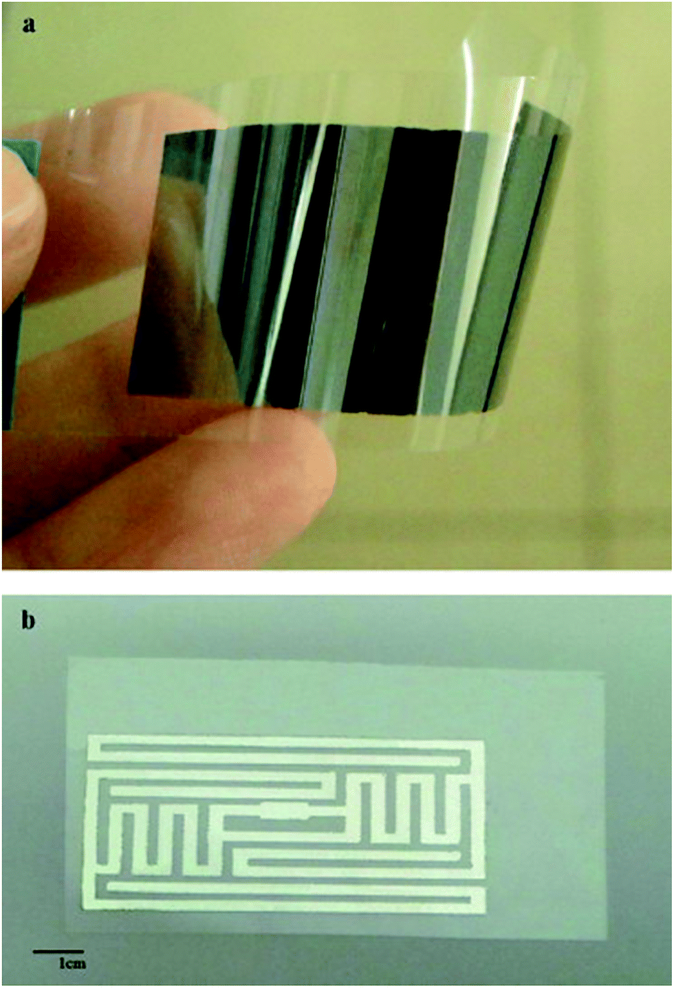 | ||
| Fig. 25 (a) Photograph of inkjet printed silver patterns on PET substrate showing the metallic luster. (b) Inkjet printed silver ink based RFID antenna. [Reprinted with permission from ref. 120 Copyright © Elsevier.] | ||
Silver inks based on different silver morphological nanostructures have been reported. Belsey et al.255 developed electrically conductive adhesives (ECAs) using a ternary hybrid of silver microflakes (AgMFs), Ag nanospheres (AgNSs), and AgNWs. Fig. 26 illustrates a ternary hybrid ECA and shows a photograph of the RFID antenna printed on the flexible polyethylene terephthalate (PET) substrate. The RFID tag consists of an antenna and a chip. Both the AgNSs and the AgNWs were found to significantly improve the electrical conductivity of the AgMF/epoxy adhesives. The optimized ternary hybrid adhesive formulation with 30 wt% AgMFs, 7.5 wt% AgNSs, and 2.5 wt% AgNWs was used to develop the RFID tag. Both the lap shear strength (LSS) and electrical conductivity of the ternary silver (AgMFs, AgNSs and AgNWs)/epoxy hybrid ECA containing 40 wt% Ag contents were higher compared with commercial ECAs that were filled with 60 wt% of AgMF contents. The ternary hybrid ECA with optimized formulation was used to print the RFID tag antennas. The ternary hybrid/epoxy adhesive was easily printed on flexible paper, polyimide (PI), and PET substrates. The RFID tag with a chip was deposited on the PET substrate and compared with a RFID tag fabricated with the commercial ECA (65 wt% AgMFs). The RFID tag showed a reading distance of 2.5 m. The lower Ag contents of 40 wt% in ternary ECA compared with commercial ECA with 65 wt% Ag led to excellent lap shear strength (LSS), which will be eventually cost effective. Therefore, the ternary (AgMFs, AgNSs, and AgNWs)/epoxy hybrid ECA is advantageous for fabricating an RFID antenna. The AgNP ink has been extensively used for fabricating RFID tag sensors.256–258
 | ||
| Fig. 26 (Left) Illustration of a ternary (AgMF, AgNS, and AgNW)/epoxy hybrid electrically conductive adhesive (ECA). (Right) Photograph of a RFID antenna printed on the PET substrate using the ternary hybrid ECA having optimized formulation. [Reprinted with permission from ref. 255 Copyright © American Chemical Society.] | ||
Copper nanoparticle-based RFID tag sensors
Silver microflake/nanoflake-based conductive inks have been widely used in printed electronics.259 However the increasing cost of silver metal has created a demand for less expensive, alternate conductive inks. The conductive inks developed from polypyrrole, AgNPs, graphene, and CNTs have been discussed above in connection with flexible electronics, particularly focused on RFID technology. Copper conductive inks also seem more attractive for printed electronics than silver inks due to their much lower cost and also high electrical conductivity.260–263 The conductive copper NP inks show a great potential for solar cells, sensors, flexible displays, and RFID tags. However, copper ink suffers from easy degradation from oxidation due to air, humidity, high temperatures, and chemicals, which limits its use in specific printed electronics applications. A coating of a protective layer over copper NPs is generally used to prevent oxidation from air and chemicals under ambient conditions.264–267 Li and Chen265 prepared Cu nano-ink for direct writing on a photo-paper with a roller pen. Fig. 27 compares the resistivity of the drawn Cu lines and bulk Cu as function of sintering time. The electrical resistivity of drawn Cu line decreased as the sintering time increased. The written Cu patterns showed resistivity of 7.2 ± 0.6 μΩ cm after sintering at 160 °C for 2 h in Ar which was 4.40 times compared with the resistivity of 1.72 μΩ cm for bulk Cu wire. The Cu-ink conductive patterns generated on a photo-paper using a roller pen after sintering at 160 °C for 2 h were able to light an ordinary small bulb. A RFID antenna was also prepared on a photo-paper from Cu conductive patterns. This demonstrated that the Cu nano-ink can be used for patterning conductive circuits on flexible and foldable photo-paper substrate for developing printed electronics. | ||
| Fig. 27 Variation of resistivity as function of sintering time of the drawn Cu lines after sintering at 160 °C for different time. [Reprinted with permission from ref. 265 Copyright © Elsevier.] | ||
In another study, Li et al.266 used poly(N-vinylpyrrolidone) (PVP) capped CuNPs for developing nano-Cu ink. The Cu conductive patterns were obtained with nano-Cu ink on an ordinary photo-paper with a roller pen after sintering at 160 °C in Ar atmosphere. The RFID antenna prepared from nano-Cu ink showed resistivity of 13.4 ± 0.4 μΩ cm which was about 8 times higher than the resistivity of 1.72 μΩ cm for bulk Cu wire. Fig. 28 shows a flexible RFID antenna drawn on photopaper with a roller ball pen filled with nano-Cu ink with and lighting of an ordinary lamp using nano-cu ink conductive patterns. The nano-Cu ink based RFID antenna has a thickness of 15 ± 0.5 μm and a width of 100 ± 0.2 μm on the photo-paper. The scanning electron microscopy (SEM) images of nano-Cu conductive patterns were recorded after sintering at different temperatures and the surface of Cu conductive patterns contained many CuNPs. The resistivity of Cu patterns decreased with increasing sintering temperature. The resistivity changed from 80 ± 2.4 μΩ cm to 21 ± 1.0 μΩ cm and then to 13.4 ± 0.4 μΩ cm after sintering at 120 °C, 140 °C. and 160 °C, respectively, due to the condensing of CuNPs into bulk Cu. The resistivity of Cu patterns was determined by the Cu microstructure generated after sintering at different temperatures. The PVP capping layer plays an important role in protecting CuNPs from oxidation.
 | ||
| Fig. 28 (a) Flexible RFID antenna printed with nano-Cu ink with on photopaper using a roller ball pen and (b) a conductive test of nano-Cu ink patterns using an ordinary lamp. [Reprinted with permission from ref. 266 Copyright © Elsevier.] | ||
Tsai et al.268 prepared antioxidative copper NP inks, and their based copper films showed a sheet resistance of 47.6 mΩ sq−1. The sheet resistance of the copper film increased from 47.6 mΩ sq−1 to 50.1 mΩ sq−1 after annealing at 250 °C. The electrically conductive copper films exhibited long-term stability without any oxidative degradation over 6 months, which was confirmed by energy-dispersive X-ray spectroscopy. The antioxidative properties and long-term stability for copper NP films originated due to the polymer protective layer coated on the copper NPs. Kanzaki et al.269 demonstrated that sintering at low temperatures at less than 150 °C could yield conductive Cu films on flexible polymer substrates from Cu-based composite inks having sub-10 nm CuNPs protected by a coating of 1-amino-2-propanol (AmIP). Oxalic acid was also used to produce antioxidative Cu films during sintering. Fig. 29 shows the change in electrical resistivity of Cu films as a function of sintering temperature between 60 °C to 120 °C and SEM images of the Cu films obtained after sintering at 80 °C. The Cu films were obtained from the composite ink having 3:1 wt% mixture of micrometer-sized Cu particles and AmIP–CuNPs in 1 wt% antioxidant oxalic acid sintered for 60 min under nitrogen atmosphere. The sintering of the AmIP–CuNPs takes place at 80 °C. The Cu films prepared after sintering the Cu-based inks at 150 °C in air for 10 s showed a resistivity of 5.5 × 10⁻⁵ Ω cm. The Cu-based composite ink showed resistivity of 5.3 × 10⁻⁵ Ω cm after sintering at 80 °C and 8.4 × 10⁻⁶ Ω cm at 120 °C. The lowest resistance of 2.6 × 10⁻⁴ Ω cm was measured for the Cu films deposited on a polyimide substrate sintered at 150 °C for 20 s. A resistance of 1.3 × 10⁻⁴ Ω cm was recorded for Cu film deposited on the flexible PET substrate. Fig. 30 shows the schematics of the sintering mechanism of the Cu-based composite inks where a simple hotplate heat treatment method was used to produce Cu conductive films of 10−5 Ω cm. The total process including casting, drying, and then sintering to produce Cu films from Cu-based composite ink on flexible plastic substrates can be accomplished in less than 1 min. This study indicated that thermal sintering of Cu-based composite inks at low temperatures could be used for printed flexible electronics.
 | ||
| Fig. 29 (a) Change in electrical resistivity of Cu films as a function of sintering temperature. (b, c) SEM images of the sintered Cu films prepared after sintering at 80 °C. [Reprinted with permission from ref. 269 Copyright © American Chemical Society.] | ||
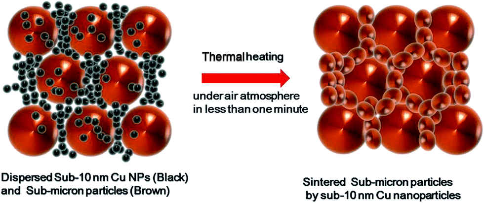 | ||
| Fig. 30 Schematic illustration of the sintering mechanism of the copper-based composite inks. [Reprinted with permission from ref. 269 Copyright © American Chemical Society.] | ||
Various methods and chemical routes have been used to prepare conductive Cu films from Cu-based inks. Dharmadasa et al.270 deposited Cu conducting films on glass and flexible PET substrates using Cu and copper oxide NPs. The 8 μm thick Cu conducting films had a sheet resistance of 0.12 Ω sq−1 over a 10 cm2 area. Farraj et al.271 formed conductive patterns on polymer substrates using Cu-formate-2-amino-2-methyl-1-propanol ink. The copper ink plasma treated at 160 W for 8 min exhibited an electrical resistivity of 7.3 ± 0.2 μΩ cm, which was 23% of the bulk copper. Fig. 31(a) shows the inkjet-printed copper patterns on a flexible poly(ethylene naphthalate) (PEN) substrate that was obtained after plasma treatment. The electrical conductivity of copper patterns was measured as a function of storage time to examine the oxidation of printed patterns. The conductivity increased by 17% after 45 days for copper patterns exposed to ambient conditions (air) and 3% increased for copper patterns stored in a sealed Petri dish. In another study, Zhang et al.272 prepared CuNPs by a chemically modified polyol process where Cu(OH)2 was used as the precursor, L-ascorbic acid as the reducing agent, and PEG-2000 as the protective layer. The synthesized copper NPs had a size distribution of 135 ± 30 nm and showed no oxidation after storing for 30 days under ambient atmospheric conditions. The CuNPs dispersed in oil-based ink could be silk-screen printed onto flexible polymer substrates and then transformed into electrically conductive patterns after annealing. The Cu films showed electrical resistivity of 15.8 μΩ cm, 10 times higher compared with bulk copper. Fig. 31(b) and (c) show the photograph of the Cu-conductive ink-based printed pattern on a polyimide substrate and a lighted LED device fabricated with copper-printed circuit board. The CuNPs prepared from Cu-based conductive ink were silk-screen printed on a flexible polymer substrate and thereafter sintered at 250 °C for 30 min. A continuous coil circuit having a width of 1 mm and a spacing of 2 mm was fabricated. The LED device was integrated into the coil circuit having printed copper patterns, which served as a conducting wire. The lighted LED showed that the copper-ink-printed electrical circuit board was functional. These studies demonstrated that highly conductive copper patterns (circuits) can be easily printed with copper inks on low-cost polymer substrates for various applications in flexible electronics.
 | ||
| Fig. 31 (a) Photograph of inkjet-printed highly conductive copper patterns on a flexible poly(ethylene naphthalate) (PEN) substrate after plasma treatment. [Reprinted with permission from ref. 271 Copyright © American Chemical Society.] (b) Photograph of the copper-conductive-ink-based printed pattern on a flexible polyimide substrate. (c) Lighted LED device connected with the copper-printed circuit board. [Reprinted with permission from ref. 272 Copyright © American Chemical Society.] | ||
The copper-ink-printed conductive patterns have been used for fabricating RFID antenna tags. The brush-painting technique has been used for printing copper and silver inks on cotton fabric, which resulted in high electrical conductivity well suited for RF electronics. The RFID tags made of the copper and silver ink antennas showed a reading range of 6 and 10 m, respectively.273 The low-cost passive UHF RFID tags have been printed on polyester-based substrate using silver and copper inks. The tag performance was compared with these two inks using polyimide substrate.274 RFID tags printed using copper-oxide-NP-based ink showed reading ranges between 3.5 and 8.5 meters.275 Barahona et al.276 prepared ultra-wide band (UWB) chipless RFID tags printed either with copper, aluminum, or silver on bond paper or PET substrates and pointed out that replacing silver by copper would reduce the cost by 96% and 65% when copper is replaced by aluminum. Kim et al.277 reported Cu-ink-based patterning conductive electrodes and fabrication of RFID antenna tags. The Cu NP inks showed the lowest electrical resistivity of 12.5 μΩ cm after sintering for 20 min at 250 °C. Printed Cu film had the adhesion strength of 5B level with a 5% epoxy resin binder. A RFID antenna was developed with Cu ink and compared with silver-paste and copper-etched antennas. Fig. 32 shows FE-SEM images of RFID antenna tags developed using silver-paste and copper ink, photograph of a copper-ink-printed RFID antenna, and a comparison of measured return loss (S11) for silver-paste and copper-ink RFID antenna tags with a conventional copper-etched RFID antenna. A loop-type RFID antenna tag was developed from copper ink on a polyimide film using the screen-printing method. The length and width of the copper-ink-printed RFID antenna tag were 2 mm. The copper-ink-printed antenna had a thickness of 1.5 mm after the sintering. The total length was 280 mm, and the number of turns was 3 for the printed antenna. The performance of these antennas was evaluated by measuring return loss (S11) as a function of resonance frequency. The copper-ink-printed RFID antenna displayed a frequency of 14.0 MHz compared with 13.7 MHz for the copper-etched antenna. The maximum return loss measured at the resonance frequency were −8.8 dB for the silver-paste-printed antenna, −14.4 dB for the copper-ink-printed antenna, and −16.8 dB for the conventional copper-etched reference antenna. The usable frequency band widths were 13.6–13.8 MHz for copper-etched and 13.4–14.7 MHz for copper-ink printed antennas for a return loss of less than −10 dB whereas the silver-paste-printed antenna had no such frequency band. Though the maximum return loss of the copper-ink-printed antenna was lower compared with the conventional copper-etched antenna, its frequency band width was broader. FE-SEM images of RFID antenna tags showed a smoother surface of the copper-ink antenna compared with the silver-paste antenna. The smaller surface roughness of 0.23 μm for the copper ink compared to that of 1.39 μm for the silver-paste antenna could lead to lower electrical resistance and high inductance for the former over that of the silver-paste antenna. Copper conductive ink can be printed on a variety of plastic substrates such as PEN, PET, PDMS, and latex as well as on textile, paper, and plywood for applications in RFID tags.278–285
 | ||
| Fig. 32 FE-SEM images of RFID antenna tags developed using silver paste (a) and copper ink (b), and cross-section image of copper-ink-printed RFID antenna. (d) Photograph of a copper-ink-printed RFID antenna. (e) Comparison of return loss (S11) as a function of resonance frequency for silver-paste and conventional copper-etched RFID antennas with copper-ink RFID antenna tags. [Reprinted with permission from ref. 277 Copyright © Elsevier.] | ||
Table 3 lists the nanomaterial-based RFID tag sensors used for detecting different gases and chemicals. The limit of detection (LOD) demonstrated by nanomaterial-based FRID tag sensors for different analytes at radio frequencies are listed. Besides these materials, RFID tag sensors have been fabricated using copper acetate ink for detecting H2S gas,286 polymer films coated on coplanar waveguides (CPWs) for detecting volatile organic compounds (VOCs),287 silicon nanowires based chipless RFID for humidity sensing in the 3.0 to 7.5 GHz band288 and other materials for anticounterfeiting,289 combinatorial screening,290 and homeland security.291 Drugs counterfeiting not only costs human lives but it also creates an extra burden on healthcare industries. You et al.292 used inkjet-printed upconversion fluorescent NPs for medicine counterfeiting. A smartphone was used for anticounterfeiting of drugs to detect an upconversion fluorescent three-dimensional (3D) quick response (QR) code. Three colored inks were formulated using upconversion fluorescent NPs having red, green, and blue (RGB) emission colors. The upconversion fluorescent 3D QR code was made of three different color layers where each color layer was encoded with drug-related information. A smartphone application was used for decoding the multicolor 3D QR code to confirm the authenticity of drugs.
| Nanomaterials | Analyte | Limit of detection | Frequency | Ref. |
|---|---|---|---|---|
| Single-walled carbon nanotubes (SWCNTs) | NH3 | 2.85 ppm | 13.56 MHz | 214 |
| SWCNTs/poly(m-aminobenzene sulfonic acid) | NH3 | 50 ppm | 3.9 GHz | 216 |
| CuO–SWCNT nanocomposite | H2S | 100 ppb | 13.56 MHz | 220 |
| Reduced graphene oxide (rGO)/Pt nanoparticles | H2 | 1 ppm | 900 MHz | 187 |
| Carbon black/organic polymer composites | NH3 | 151 ppm | 13.56 MHz | 212 |
| Toluene | 37.3 ppm | 13.56 MHz | 212 | |
| Ethanol | 77.5 ppm | 13.56 MHz | 212 | |
| Water | 31.3 ppm | 13.56 MHz | 212 | |
| Hydrogel-coated pH-electrode | NH3 | 1.5 ppm | 6 MHz | 217 |
| Carboxylated polypyrrole nanoparticles (C-PPy NPs) | NH3 | 0.1 ppm | 900 MHz | 164 |
| Copper acetate ink/paper substrate | H2S | 5 ppm | 2.8 GHz | 286 |
| Copolymer films on coplanar waveguides (CPWs) | Ethanol | 600 ppm | 9.29 GHz | 287 |
| Acetone | 270 ppm | 9.29 GHz | 287 | |
| Isopropyl | 330 ppm | 9.29 GHz | 287 |
Gold nanoparticle-based lnk
In addition to silver and copper inks, gold nanoparticles-based ink has been used for inkjet printing of flexible electronics.293–302 Huang et al.293 used hexanethiol-encapsulated gold nanocrystals for printing circuits on a flexible polyester substrate. The inkjet printed 1.5 nm gold nanocrystal conductive patterns showed a sheet resistance of >0.03 Ω sq−1 after sintered at 150 °C which was 70% that of bulk gold. The printed gold conductive patterns showed 6 times higher resistivity after laser sintering compared with bulk gold.294 In another study, inkjet printed 50 layers of AuNP ink sintered at 500 °C for 3 h showed resistivity of 12.5 μΩ cm.295 The PVP and acrylic resin double layer capped AuNP ink showed stability over one year against aggregation at 20% gold concentration. The reactive inkjet printing (RIP) technique has been used to control the size of self-assembled AuNPs on glass and silicon substrates through adjusting the concentration of the gold precursor in different solvent systems.296 The gold precursor prepared in a solvent system containing dimethyl sulfoxide (DMSO) and oleylamine in 1,2-dichlorobenzene was found to be most suitable for printing uniform size AuNPs using RIP technique. The AuNPs and gold molecular precursor inks have been used for inkjet-printing of gold conductive patterns on different substrates.297–302RFID technology has tremendous potential to grow into a multi-billion dollar industry within the next decade. Many applications of RFID tag sensors are emerging, such as monitoring fish freshness,303 supply chains,304 wearable healthcare,305,306 crack detection,307 wearable healthcare,308 tracking lost visitors in theme parks,309 monitoring prisoners,310 denim production,311 animal tracking in medical studies,312 counterfeit drugs,313 asset management,314 etc. Furthermore, the integration of RFID tag sensors with the Internet and cloud computing will substantially advance e-healthcare applications as well as many other research areas with an economic boost in IoT worldwide.315–317
Stability of inkjet printed conductive patterns
The long-term stability of inkjet-printed conductive patterns is significant for the performance of electronic devices. The discontinuation of printed patterns as well as gradual degradation of metallic conductive patterns over time could lead to device failure. Therefore, long-term durability of inkjet inks and printed conductive patterns depend upon a number of factors such as chemical formulations of conductive inks, capping and dispersion agents, printing method, substrate temperature, sintering, and the morphological structures of printed conductive patterns. Derby318 discussed the physical processes of inkjet printing and how the properties of the viscoelastic fluid precursors influence the interactions between individual ink droplets and the substrate to be used for printing, therefore define the resolution and precision of printed patterns. Both conductive patterning and the structure of substrates contribute to the quality of print resolution. The inkjet droplet spacing and contact angle both play an important role in the stability of conductive printed patterns.319 Li et al.266 used capping agent PVP as a coating to protect copper nanoparticles against oxidation. Chen et al.124 studied stability of silver ink. The silver diethanolamine (DEA) inks were stored at different temperatures including 5, 20, and 70 °C. The silver ink was transparent for 8 days at 5 °C, whereas aggregates appeared after sintering at 70 °C for 1 h and silver thin film formed by after sintering silver ink on the PET substrate at 70 °C for 1 h. Kwon et al.320 developed 3D complementary organic field-effect transistor (COFET) where source/drain/gate electrodes, organic semiconductor layers and interconnections were all inkjet-printed except the CVD deposited parylene dielectric. The array of inkjet printed 3D devices showed uniformity with 100% yield, 45.8% noise level and long-term stability of the electronic devices over a period of 8 months under ambient conditions without any encapsulation.The stability of inkjet printed conductive patterns has been studied over extended period of time. Nie et al.120 studied the long-term stability of silver citrate precursor based conductive inkjet ink. Fig. 33 shows the photographs of silver citrate conductive inkjet inks stored in a refrigerator and under ambient conditions for 60 days and the variation of electrical resistivity of inkjet-printed silver patterns on flexible PET substrate as a function of storage time of the silver ink in the refrigerator and under ambient conditions. The inkjet-printed silver patterns were sintered at 150 °C for 50 min. The freshly prepared silver citrate conductive ink was slightly yellowish and transparent while ink stored in the refrigerator for a period of 60 days showed no change in color. However, slight change in color was observed for the ink stored under ambient conditions at 25 °C for 60 days without any type of precipitation. The long-term stability of these silver citrate conductive inks was also evaluated by measuring the electrical resistivity of the inkjet-printed silver patterns after sintering at 150 °C for 50 min. The silver printed patterns showed long-term stability because no noticeable change in electrical resistivity was observed up to 60 days. Li and Chen265 recorded X-ray diffraction patterns of as-prepared CuNPs at 80 °C and CuNPs stored in a capped bottle under atmospheric conditions for a period of 6 months which showed similar XRD patterns. The cetyltrimethylammonium bromide (CTAB) capping layer created a diffusion barrier over CuNPs providing stability against oxidation. Furthermore oxidation of CuNPs was also prevented by the hydrazine reducing agent. Secor et al.321 prepared inkjet-printed indium–gallium–zinc-oxide (IGZO) transistors by embedding the graphene electrodes. The IGZO based inkjet-printed TFTs showed an electron mobility of 6 cm2 V−1 s−1, on/off current ratio of 105 and long-term stability for 365 days under dark ambient conditions without any degradation. The stability of inkjet printed conductive patterns of CuNPs,267,279 silver,322–325 Cu–Ag core–shell nanoparticles326 and other inks have been reported.327–330 Jeong et al.324 used poly(acrylic acid) (PAA) sodium salt both as a capping agent and dispersant for aqueous silver inks to introduce long-term dispersion stability. The capping agents such as PVP, PAA, CTAB, etc., have been used as a protecting layer on metallic nanoparticles for developing inkjet inks. The chemical formulations of inkjet inks, substrate processing, printing method, sintering technique and temperature, all these factors contribute to the fine resolution and stability of printed conductive patterns. The stability of inkjet metallic and molecular precursor inks as well as the stability of printed conductive patterns against oxidation under ambient conditions is important for printed electronics.
 | ||
| Fig. 33 Stability of silver citrate conductive inkjet ink up to 60 days. (a) Photographs showing silver citrate conductive inkjet inks: (1) freshly prepared inkjet ink; (2) silver citrate ink stored in a refrigerator for 60 days; (3) silver citrate ink stored under ambient conditions at 25 °C for 60 days; (b) the variation of electrical resistivity of printed silver patterns on flexible PET substrate sintered at 150 °C for 50 min as a function of storage time of the silver ink in the refrigerator and under ambient conditions. [Reprinted with permission from ref. 120 Copyright © Elsevier.] | ||
Conclusion
The RFID tag sensors based on polypyrrole, graphene, silver and copper NPs, carbon nanotubes which were inkjet-printed on a variety of surfaces such as plastic, textile, paper, and even metallic surfaces show potential in flexible and wearable electronics technologies. The challenges such as the impact of RF radiation on human health, security, and energy requirements for RFID security are real issues. The potential risk of RFID technology on human health should be addressed because nanomaterials as well as RF frequency may impact physiological activities.331,332 The safety of RFID has been studied. Kim et al.333 studied the effect of 915 MHz RFID exposure in rats where no change in thyroid secretory function in connection with triiodothyronine (T3), thyroxine (T4), and thyroid-stimulating hormone (TSH) was observed in sham-exposed and RFID exposed rats. Paik et al.334 reported that 915 MHz RFID exposure alters urinary polyamines (PAs) in rats. The level of N1-acetylspermine was found to be 54% higher after RFID exposure whereas it increased 17% in the sham group. Lai et al.335 studied the effect of implanted RFID microchips on human cancer cells by analyzing the emitted RF energy. Three different types of cancer cells, including BT474 breast cancer, Molt-4 leukemia, and HepG2 hepatic, were exposed for a period of 1 h to RFID microchip-emitted RF field. The RF energy emitted by microchips inhibited the growth/killed all three types of cancer cells. This opens a new approach of cancer treatment by implanting RFID microchips in tumors. More studies should be conducted to access the real impact of RFID technology on the human health.One of the requirements for IoT devices is a continuous supply of sufficient energy provided either through the batteries or semiconductor solar cells by harvesting energy from the sun. Therefore IoT devices having a long lifetime with low-power consumption are ideal candidates. Blaauw et al.336 pointed out that μW to mW average power is required for larger-scale IoT devices, whereas nW power will be sufficient for millimeter-size IoT devices. They also discussed the desired lifetime and size of alkaline AA, 20 mm Li-ion, 90 mm2 Li–polymer, and 1 mm2 Li thin-film batteries in terms of maximum power drawn. IoT devices must harvest sufficient energy in order to operate up to several years. It was suggested that a 4 V battery can be charged from the 1 mm2 solar cell under dim light in an indoor environment. IoT devices based on low-power consumption and modular designs should be developed. The fabrication of millimeter sensor systems from a set of eight die chips has been demonstrated. Huang et al.193 reported that a chemically sensitive graphene field-effect transistor (GFET) device can operate on very low power of 10 μW (0.1 V × 0.1 mA), which is also compatible with Wi-Fi and Bluetooth® communication systems. This graphene nanosensor-based IoT system also uses smartphones and cloud computing technology. Janeczek et al.337 showed that using a NFC-enabled smartphone, very low power of 8.5 mW was consumed by the RFID tag while performing multigas sensing activity with NFC/RFID tag sensor. Energy requirements for RFID tags should be considered where nanogenerators or solar cells may become important part of RFID technology as a clean energy source.
Flexible RFID tags sensors should become an integral part of wearable electronic devices, which is a growing industry, from smart watches to smartphones for health monitoring.338–341 The integration of IoT with nanotechnology will have an impact on future emerging technologies and their applications over the entire spectrum of IoT-related sectors. The IoNTs based on nanoelectronics, nanomedicine, solar cells, sensors, food products, health and transport industries will gain attention over the next decade. RFID-based systems could supercede barcode industries for IoT applications within the next decade. The challenges and issues related to energy and safety should be considered to explore the full potential of RFID tag sensors in IoNT-based technologies.
Conflicts of interest
The authors declare no conflicts of interest.References
- G. Cummins and M. P. Desmulliez, Circuit World, 2012, 38, 193–213 CrossRef CAS.
- M. Singh, H. M. Haverinen, P. Dhagat and G. E. Jabbour, Adv. Mater., 2010, 22, 673–685 CrossRef CAS PubMed; R. E. Saunders and B. Derby, Int. Mater. Rev., 2014, 59, 430–448 CrossRef.
- S. Kim, C. Mariotti, F. Alimenti, P. Mezzanotte, A. Georgiadis, A. Collado, L. Roselli and M. M. Tentzeris, IEEE Microw. Mag., 2013, 14, 66–77 CrossRef.
- I. Lee and K. Lee, Bus. Horiz., 2015, 58, 431–440 CrossRef.
- K. Tillman, http://blogs.cisco.com/news/cisco-connections-counter, accessed 3 June 2017.
- J. Manyika, M. Chui, P. Bisson, J. Woetzel, R. Dobbs, J. Bughin and D. Aharon, http://www.mckinsey.com/business-functions/digital-mckinsey/our-insights/the-internet-of-things-the-value-of-digitizing-the-physical-world, accessed June 2015.
- Handbook of Nanostructured Materials and Nanotechnology, ed. H. S. Nalwa, Academic Press, San Diego, 1999, vol. 1–5 Search PubMed.
- Encyclopedia of Nanoscience and Nanotechnology, ed. H. S. Nalwa, American Scientific Publishers, Los Angeles, 2004, vol. 1–10 Search PubMed.
- Handbook of Nanostructured Biomaterials and Their Applications in Nanobiotechnology, ed. H. S. Nalwa, American Scientific Publishers, Los Angeles, 2005, vol. 1–2 Search PubMed.
- S. E. Lyshevski, Nano and Molecular Electronics Handbook, CRC Press, Boca Raton, 2016 CrossRef CAS PubMed; A. Vilan and D. Cahen, Chem. Rev., 2017, 117, 4624–4666 CrossRef CAS PubMed; R. Puers, L. Baldi, M. Van de Voorde and S. E. van Nooten, Nanoelectronics: Materials, Devices, Applications, John Wiley & Sons, New York, 2017, vol. 1–2 Search PubMed.
- Z. Pei, Z. Li and X. Zheng, J. Nanosci. Nanotechnol., 2016, 16, 9028–9049 CrossRef CAS; S. Wu, Y. Du and S. Sun, Chem. Eng. J., 2017, 307, 189–207 CrossRef.
- S. Rajbhandari, J. J. McKendry, J. Herrnsdorf, H. Chun, G. Faulkner, H. Haas, I. M. Watson, D. O'Brien and M. D. Dawson, Semicond. Sci. Technol., 2017, 32, 023001 CrossRef CAS; M. Yan, Q. Zhang, Y. Zhao, J. Yang, T. Yang, J. Zhang and X. A. Li, J. Nanosci. Nanotechnol., 2015, 15, 6279–6294 CrossRef PubMed.
- S. Feng, Z. Lin, X. Gan, R. Lv and M. Terrones, Nanoscale Horiz., 2017, 2, 72–80 RSC; Y. Wang and S. Hu, J. Nanosci. Nanotechnol., 2016, 16, 7852–7872 CrossRef CAS.
- M. I. Kim and Y.-S. Lee, J. Nanosci. Nanotechnol., 2016, 16, 4310–4319 CrossRef CAS PubMed.
- I. Choi, J. Nanosci. Nanotechnol., 2016, 16, 4274–4283 CrossRef CAS PubMed.
- M. A. Robles-García, F. Rodríguez-Félix, E. Márquez-Ríos, J. A. Aguilar, A. Barrera-Rodríguez, J. Aguilar, S. Ruiz-Cruz and C. L. Del-Toro-Sánchez, J. Nanosci. Nanotechnol., 2016, 16, 8188–8207 CrossRef.
- Cancer Nanotechnology: Nanomaterials for Cancer Diagnosis and Therapy, ed. H. S. Nalwa and T. J. Webster, American Scientific Publishers, Los Angeles, 2007 CrossRef CAS PubMed; D. J. Joe, J. Hwang, C. Johnson, H.-Y. Cha, J.-W. Lee, X. Shen, M. G. Spencer, S. Tiwari and M. Kim, J. Nanosci. Nanotechnol., 2016, 16, 144–151 CrossRef CAS PubMed; R. Ahmad, J. Fu, N. He and S. Li, J. Nanosci. Nanotechnol., 2016, 16, 67–80 CrossRef PubMed; J. Xu, X. Zhou, Y. Li and Y. Tian, Curr. Drug Metab., 2017, 18, 266–279 CrossRef PubMed; J. Shi, P. W. Kantoff, R. Wooster and O. C. Farokhzad, Nat. Rev. Cancer, 2017, 17, 20–37 CrossRef PubMed.
- M. Ramalingam, A. E. Haj, T. J. Webster and S. Ramakrishna, J. Nanosci. Nanotechnol., 2016, 16, 8859–8861 CrossRef CAS; S. Hu, Y. Zeng, S. Yang, H. Qin, H. Cai and J. Wang, J. Nanosci. Nanotechnol., 2015, 15, 6327–6341 CrossRef PubMed; J. H. An, S. U. Kim, M.-K. Park and J. W. Choi, J. Nanosci. Nanotechnol., 2015, 15, 7929–7934 CrossRef PubMed; S. Ahadian, R. Obregón, J. Ramón-Azcón, G. Salazar, H. Shiku, M. Ramalingam and T. Matsue, J. Nanosci. Nanotechnol., 2016, 16, 8862–8880 CrossRef; K. I. Budhwani, A. T. Wood, A. Gangrade, P. Sethu and V. Thomas, J. Nanosci. Nanotechnol., 2016, 16, 8923–8934 CrossRef; V. N. Vernekar, R. James, K. J. Smith and C. T. Laurencin, J. Nanosci. Nanotechnol., 2016, 16, 8953–8965 CrossRef; W. F. Schmidt and S. Singh, J. Nanosci. Nanotechnol., 2014, 14, 1–14 CrossRef PubMed.
- D. Singh, A. P. Minz and S. K. Sahoo, Drug Discovery Today, 2017, 22, 952–959 CrossRef CAS PubMed; S. Singh, J. Nanosci. Nanotechnol., 2010, 10, 7906–7918 CrossRef PubMed; R. Singh and H. S. Nalwa, J. Biomed. Nanotechnol., 2011, 7, 489–503 CrossRef PubMed; H. S. Nalwa, J. Biomed. Nanotechnol., 2014, 10, 1635–1640 CrossRef PubMed; H. S. Nalwa, J. Biomed. Nanotechnol., 2014, 10, 2421–2423 CrossRef PubMed.
- F. Dressler and S. Fischer, Nano Commun. Netw., 2015, 6, 29–38 CrossRef; A. Nayyar, V. Puri and D.-N. Le, Nanosci. Nanotechnol., 2017, 7, 4–8 Search PubMed; I. Akyildiz, M. Pierobon, S. Balasubramaniam and Y. Koucheryavy, IEEE Comm. Mag., 2015, 53, 32–40 CrossRef; S. Balasubramaniam and J. Kangasharju, Computer, 2013, 46, 62–68 CrossRef.
- C. M. Roberts, Comput Secur., 2006, 25, 18–26 CrossRef.
- V. D. Hunt, A. Puglia and M. Puglia, RFID: A Guide to Radio Frequency Identification, John Wiley & Sons, New York, 2007 Search PubMed.
- D. Brown, RFID Implementation, McGraw-Hill Education, New York, 2007 Search PubMed.
- K. Finkenzeller, RFID Handbook: Fundamentals and Applications in Contactless Smart Cards, Radio Frequency Identification and Near-Field Communication, John Wiley & Sons, New York, 2010 Search PubMed.
- S. A. Ahson and M. Ilyas, RFID Handbook: Applications, Technology, Security, and Privacy, CRC Press, Boca Raton, 2008 Search PubMed.
- M. van Lieshout, L. Grossi, G. Spinelli, S. Helmus, L. Kool, L. Pennings, R. Stap, T. Veugen, B. van der Waaij and C. Borean, in RFID Technologies: Emerging Issues, Challenges and Policy Options, ed. I. Maghiros, P. Rotter and M. V. Lieshout, European Commission, Directorate-General Joint Research Centre, Institute for Prospective Technological Studies, Luxembourg, 2007 Search PubMed.
- P. Escobedo, M. A. Carvajal, L. F. Capitán-Vallvey, J. Fernández-Salmerón, A. Martínez-Olmos and A. J. Palma, Sensors, 2016, 16, 1085 CrossRef PubMed.
- J. F. Salmerón, A. Rivadeneyra, M. Agudo-Acemel, L. F. Capitán-Vallvey, J. Banqueri, M. A. Carvajal and A. J. Palma, Sens. Actuators, A, 2014, 220, 281–289 CrossRef.
- M. Ward, R. Van Kranenburg and G. Backhouse, JISC Technology and Standards Watch, 2006, 5, 10 Search PubMed.
- S. Zuffanelli, P. Aguila, G. Zamora, F. Paredes, F. Martin and J. Bonache, Sensors, 2016, 16, 1150 CrossRef PubMed.
- K. Ashton, RFID Journal, 2009, 22, 97–114 Search PubMed.
- X. Jia, Q. Feng, T. Fan and Q. Lei, in 2nd International Conference on Consumer Electronics, Communications and Networks (CECNet), IEEE, Yichang, China, 2012, pp. 1282–1285 CrossRef PubMed; T. M. Fernández-Caramés, P. Fraga-Lamas, M. Suárez-Albela and L. Castedo, Sensors, 2017, 17, 28 CrossRef PubMed.
- S. Naskar, P. Basu and A. K. Sen, in The Internet of Things in the Modern Business Environment, ed. I. Lee, IGI Global, Hershey, PA, 2017, pp. 1–27 CrossRef; A. S. Kohli and C. Peng, Int. J. Inform. Syst. Supply Chain Manag., 2017, 10, 24–43 CrossRef.
- C. Sun, AASRI Procedia, 2012, 1, 106–111 CrossRef.
- R. R. Oliveira, I. M. Cardoso, J. L. Barbosa, C. A. da Costa and M. P. Prado, Expert. Syst. Appl., 2015, 42, 6082–6097 CrossRef.
- E. Bottani, G. Ferretti, R. Montanari and A. Rizzi, Int. J. RF Technol. Res. Appl., 2009, 1, 225–252 Search PubMed.
- B. Yan and G. Huang, in ISECS International Colloquium on Computing, Communication, Control, and Management, IEEE, Sanya, China, 2009, vol. 4, pp. 166–169 Search PubMed.
- L. Cui, J. Deng, F. Liu, Y. Zhang and M. Xu, J. Cleaner Prod., 2017, 142, 2028–2044 CrossRef.
- R. Yan and R. Yan, Ind. Manag. Data Syst., 2017, 117, 729–741 CrossRef.
- Z. Wang, H. Hu and W. Zhou, Comput. Aided Civ. Infrastruct. Eng., 2017, 32, 499–514 CrossRef.
- G. S. Lorite, T. Selkälä, T. Sipola, J. Palenzuela, E. Jubete, A. Viñuales, G. Cabañero, H. J. Grande, J. Tuominen, S. Uusitalo, L. Hakalahti, K. Kordas and G. Toth, J. Food Eng., 2017, 193, 20–28 CrossRef.
- A. C. Cagliano, A. C. Cagliano, A. De Marco, A. De Marco, C. Rafele and C. Rafele, Business Process Management Journal, 2017, 23, 47–70 CrossRef.
- S. Mathaba, M. Adigun, J. Oladosu and O. Oki, J. Intell. Fuzzy Syst., 2017, 32, 3091–3101 CrossRef.
- A. Musa and A.-A. A. Dabo, Global J. Flexible Syst. Manag., 2016, 17, 189–228 CrossRef.
- W. Zhou, S. Piramuthu, F. Chu and C. Chu, Decis. Support Syst., 2017, 98, 99–112 CrossRef.
- J. Mašek, P. Kolarovszki and J. Čamaj, Procedia Eng., 2016, 134, 231–236 CrossRef.
- X. Tan, M. Dong, C. Wu, K. Ota, J. Wang and D. W. Engels, IEEE Access, 2017, 5, 3044–3054 CrossRef.
- T. K. Mackey and G. Nayyar, Expert Opin. Drug Saf., 2017, 16, 587–602 CrossRef PubMed.
- F. Bibi, C. Guillaume, N. Gontard and B. Sorli, Trends Food Sci. Technol., 2017, 62, 91–103 CrossRef CAS.
- R. A. Potyrailo and C. Surman, Sens. Actuators, B, 2013, 185, 587–593 CrossRef CAS PubMed; R. A. Potyrailo, N. Nagraj, Z. Tang, F. J. Mondello, C. Surman and W. Morris, J. Agric. Food Chem., 2012, 60, 8535–8543 CrossRef PubMed.
- C.-Y. Tsai, M.-H. Li and R.-J. Kuo, Comput. Ind. Eng., 2017, 106, 192–204 CrossRef.
- D. Oosterlinck, D. F. Benoit, P. Baecke and N. Van de Weghe, Appl. Geogr., 2017, 78, 55–65 CrossRef.
- Y. Chen, Z. Zheng, M. Gong and F. Yu, Sensors, 2017, 17, E867 CrossRef PubMed.
- B. Lecat, J. Brouard and C. Chapuis, Br. Food J., 2017, 119, 84–104 CrossRef.
- M. Buzzi and C. Senette, in Sensing the Past: From Artifact to Historical Site, ed. N. Masini and F. Soldovieri, Springer International Publishing, Berlin, 2017, pp. 435–451 Search PubMed.
- C. G. Meyer, Bull. Mar. Sci., 2017, 93, 301–318 CrossRef.
- R. Parada and J. Melia-Segui, IEEE Comm. Mag., 2017, 55, 56–61 CrossRef.
- L. Ruiz-Garcia and L. Lunadei, Comput. Electron. Agr., 2011, 79, 42–50 CrossRef.
- S. Amendola, R. Lodato, S. Manzari, C. Occhiuzzi and G. Marrocco, IEEE Internet of Things Journal, 2014, 1, 144–152 CrossRef.
- A. Manzoor, Int. J. User-Driven Healthcare, 2016, 6, 21–45 CrossRef.
- H. Ma and K. Wang, WIT Trans. Eng. Sci., 2016, 113, 209–216 Search PubMed.
- M. Gaynor and J. Waterman, Health Policy Technol., 2016, 5, 357–369 CrossRef.
- A. D'Andrea, F. Ferri and P. Grifoni, Int. J. Comput. Clin. Practice, 2016, 1, 15–27 CrossRef.
- M. Premkumar, M. Girish and I. Karthikiran, Automation and Autonomous System, 2016, 8, 198–201 Search PubMed.
- A. Manzoor, Int. J. Inform. Comm. Tech. Hum. Dev., 2016, 8, 26–46 CrossRef.
- R. Baptista, G. Morris, R. Jones, N. Ridley, G. Kushinga, A. Arshad, J. Douglas, A. Ricketts and D. Moss, Cytotherapy, 2017, 19, S122 CrossRef.
- A. A. A. Asaimi, M. I. Razzak and R. Alshammari, Adv. Sci. Lett., 2016, 22, 2759–2763 CrossRef.
- A. Dey, A. Dey, B. Vijayaraman, B. Vijayaraman, J. H. Choi and J. H. Choi, Management Research Review, 2016, 39, 399–424 CrossRef.
- A. Cangialosi, J. E. Monaly Jr and S. C. Yang, IEEE Comm. Mag., 2007, 45, 18–23 CrossRef.
- S. Kumar, G. Livermont and G. McKewan, Tech. Health Care., 2010, 18, 31–46 Search PubMed.
- J. Zhang, G. Y. Tian, A. M. J. Marindra, A. I. Sunny and A. B. Zhao, Sensors, 2017, 17, 265 CrossRef PubMed.
- N. Kumar, K. Kaur, S. C. Misra and R. Iqbal, Peer-to-Peer Netw. Appl., 2016, 9, 824–840 CrossRef.
- C.-H. Cheng and Y.-H. Kuo, Flex. Serv. Manuf. J., 2016, 28, 593–616 CrossRef.
- K.-H. Eom, C. W. Lee, N. T. Van, K. K. Jung, J. W. Kim and W. S. Choi, International Journal of Multimedia and Ubiquitous Engineering, 2013, 8, 213–222 CrossRef.
- J. Vastl, T. Wang, T. B. Trinh and D. A. Spiegel, ACS Comb. Sci., 2017, 19, 255–261 CrossRef CAS PubMed.
- B. Shao, Doctoral Dissertation, KTH Royal Institute of Technology, Stockholm, Sweden, 2014.
- B. Shao, Q. Chen, R. Liu and L. R. Zheng, Microw. Opt. Tech. Lett., 2012, 54, 226–230 CrossRef.
- B. Shao, Y. Amin, Q. Chen, R. Liu and L.-R. Zheng, IEEE Antenn. Wireless Propag. Lett., 2013, 12, 325–328 CrossRef.
- B. Shao, Q. Chen, Y. Amin, R. Liu and L.-R. Zheng, Ann. Telecommun., 2013, 68, 401–413 CrossRef.
- N. C. Karmakar, E. M. Amin and J. K. Saha, Chipless RFID Sensors, John Wiley & Sons, New York, 2016 Search PubMed.
- S. Preradovic, I. Balbin, N. C. Karmakar and G. F. Swiegers, IEEE Trans. Microwave Theory Tech., 2009, 57, 1411–1419 CrossRef.
- Y. Feng, L. Xie, Q. Chen and L.-R. Zheng, IEEE Sens. J., 2015, 15, 3201–3208 CrossRef.
- A. Habib, R. Asif, M. Fawwad, Y. Amin, J. Loo and H. Tenhunen, IEICE Electron. Express, 2017, 14, 20170169 CrossRef.
- T. Noor, A. Habib, Y. Amin, J. Loo and H. Tenhunen, Electron. Lett., 2016, 52, 620–622 CrossRef CAS.
- M. Oliveros, M. Carminati, A. Zanutta, T. Mattila, S. Jussila, K. Nummila, A. Bianco, G. Lanzani and M. Caironi, Sens. Actuators, B, 2016, 223, 839–845 CrossRef CAS.
- M. H. Zarifi, S. Deif and M. Daneshmand, Sens. Actuators, A, 2017, 261, 24–29 CrossRef CAS.
- D. Betancourt, R. Nair, K. Haase, G. Schmidt, M. Bellmann, D. Höft, A. Hübler and F. Ellinger, in 9th European Conference on Antennas and Propagation (EuCAP), IEEE, Lisbon, Portugal, 2015, pp. 1–5 Search PubMed.
- N. Javed, A. Habib, Y. Amin and H. Tenhunen, in International Conference on Communication, Computing and Digital Systems (C-CODE), IEEE, Islamabad, Pakistan, 2017, pp. 71–74 Search PubMed.
- C. N. Verdouw, J. Wolfert, A. J. M. Beulens and A. Rialland, J. Food Eng., 2016, 176, 128–136 CrossRef.
- A. S. Voulodimos, C. Z. Patrikakis, A. B. Sideridis, V. A. Ntafis and E. M. Xylouri, Comput. Electron. Agr., 2010, 70, 380–388 CrossRef.
- H. Xin and K. Liu, Animal Frontiers, 2017, 7, 24–31 CrossRef.
- B. Yan, P. Shi and G. Huang, Trans. Chin. Soc. Agric. Eng., 2013, 29, 172–183 Search PubMed.
- S. Piramuthu and W. Zhou, RFID and Sensor Network Automation in the Food Industry: Ensuring Quality and Safety Through Supply Chain Visibility, Wiley, Chichester, 2016 Search PubMed.
- H. Cai, B. Xu, L. Jiang and A. V. Vasilakos, IEEE Internet of Things Journal, 2017, 4, 75–87 Search PubMed.
- C. Yang, Q. Huang, Z. Li, K. Liu and F. Hu, Int. J. Digital Earth, 2017, 10, 13–53 CrossRef.
- A. Botta, W. De Donato, V. Persico and A. Pescapé, in International Conference on Future Internet of Things and Cloud (FiCloud), IEEE, Barcelona, Spain, 2014, pp. 23–30 Search PubMed.
- A. Botta, W. De Donato, V. Persico and A. Pescapé, Future Generat. Comput. Syst., 2016, 56, 684–700 CrossRef.
- K. Hwang, J. Dongarra and G. C. Fox, Distributed and Cloud Computing: From Parallel Processing to the Internet of Things, Morgan Kaufmann/Elsevier, Amsterdam, 2013 Search PubMed.
- F. Tao, Y. Cheng, L. Da Xu, L. Zhang and B. H. Li, IEEE Trans. Industr. Inform., 2014, 10, 1435–1442 CrossRef.
- J. H. Abawajy and M. M. Hassan, IEEE Comm. Mag., 2017, 55, 48–53 CrossRef.
- H. E. El-Din and D. H. Manjaiah, in Internet of Things: Novel Advances and Envisioned Applications, ed. D. P. Acharjya and M. K. Geetha, Springer International Publishing, Berlin, 2017, pp. 299–311 Search PubMed.
- M. B. Mollah, M. A. K. Azad and A. Vasilakos, IEEE Cloud Computing, 2017, 4, 34–42 CrossRef.
- P. Kassal, I. M. Steinberg and M. D. Steinberg, Sens. Actuators, B, 2013, 184, 254–259 CrossRef CAS.
- M. Gao, L. Li and Y. Song, J. Mater. Chem. C, 2017, 5, 2971–2993 RSC.
- M. Liu, J. Wang, M. He, L. Wang, F. Li, L. Jiang and Y. Song, ACS Appl. Mater. Interfaces, 2014, 6, 13344–13348 CAS.
- P. Dzik, M. Veselý, M. Kete, E. Pavlica, U. L. Štangar and M. Neumann-Spallart, ACS Appl. Mater. Interfaces, 2015, 7, 16177–16190 CAS.
- P. Dzik, M. Veselý, M. Blašková, M. Králová and M. Neumann-Spallart, J. Appl. Electrochem., 2015, 45, 1265–1276 CrossRef CAS.
- S. S. Delekta, A. D. Smith, J. Li and M. Östling, Nanoscale, 2017, 9, 6998–7005 RSC.
- M. R. Beaulieu, N. R. Hendricks and J. J. Watkins, ACS Photonics, 2014, 1, 799–805 CrossRef CAS.
- E. Sowade, T. Blaudeck and R. R. Baumann, Cryst. Growth Des., 2016, 16, 1017–1026 CAS.
- H. Ding, C. Zhu, L. Tian, C. Liu, G. Fu, L. Shang and Z. Gu, ACS Appl. Mater. Interfaces, 2017, 9, 11933–11941 CAS.
- H. Nam, K. Song, D. Ha and T. Kim, Sci. Rep., 2016, 6, 30885 CrossRef CAS PubMed.
- H. Jiang, S. Alan, H. Shahbazbegian, J. N. Patel and B. Kaminska, ACS Nano, 2016, 10, 10544–10554 CrossRef CAS PubMed.
- R. P. Tortorich and J.-W. Choi, Nanomaterials, 2013, 3, 453–468 CrossRef CAS PubMed; H. J. Gysling, Curr. Opin. Colloid Interface Sci., 2014, 19, 155–162 CrossRef; S. Rondeau-Gagné and J.-F. Morin, Chem. Soc. Rev., 2014, 43, 85–98 RSC; Z. Li, A. Rahtu and R. G. Gordon, J. Electrochem. Soc., 2006, 153, C787–C794 CrossRef; J. L. Zhuang, D. Ar, X. J. Yu, J. X. Liu and A. Terfort, Adv. Mater., 2013, 25, 4631–4635 CrossRef PubMed.
- A. Kamyshny, J. Steinke and S. Magdassi, Open Appl. Phys. J., 2011, 4, 19–36 CrossRef CAS.
- C.-L. Lee, K.-C. Chang and C.-M. Syu, Colloids Surf., A, 2011, 381, 85–91 CrossRef CAS.
- H.-H. Lee, K.-S. Chou and K.-C. Huang, Nanotechnology, 2005, 16, 2436 CrossRef CAS PubMed.
- D. Kim and J. Moon, Electrochem. Solid-State Lett., 2005, 8, J30–J33 CrossRef CAS.
- K. Black, J. Singh, D. Mehta, S. Sung, C. J. Sutcliffe and P. R. Chalker, Sci. Rep., 2016, 6, 20814 CrossRef CAS PubMed.
- X. Nie, H. Wang and J. Zou, Appl. Surf. Sci., 2012, 261, 554–560 CrossRef CAS.
- Y. Dong, X. Li, S. Liu, Q. Zhu, J.-G. Li and X. Sun, Thin Solid Films, 2015, 589, 381–387 CrossRef CAS.
- L. Shen, J. Liu, X. Zeng and Z. Ren, J. Electron. Mater., 2015, 44, 720–724 CrossRef CAS.
- S. F. Jahn, T. Blaudeck, R. R. Baumann, A. Jakob, P. Ecorchard, T. Rüffer, H. Lang and P. Schmidt, Chem. Mater., 2010, 22, 3067–3071 CrossRef CAS.
- S.-P. Chen, Z.-K. Kao, J.-L. Lin and Y.-C. Liao, ACS Appl. Mater. Interfaces, 2012, 4, 7064–7068 CAS.
- J.-T. Wu, S. L.-C. Hsu, M.-H. Tsai and W.-S. Hwang, J. Phys. Chem. C, 2011, 115, 10940–10945 CAS.
- J. Li, V. Mishukova and M. Östling, Appl. Phys. Lett., 2016, 109, 123901 CrossRef CAS; K.-H. Choi, J. Yoo, C. K. Lee and S.-Y. Lee, Energy Environ. Sci., 2016, 9, 2812–2821 Search PubMed.
- Y. Li, L. Lan, P. Xiao, S. Sun, Z. Lin, W. Song, E. Song, P. Gao, W. Wu and J. Peng, ACS Appl. Mater. Interfaces, 2016, 8, 19643–19648 Search PubMed; C. M. Homenick, R. James, G. P. Lopinski, J. Dunford, J. Sun, H. Park, Y. Jung, G. Cho and P. R. Malenfant, ACS Appl. Mater. Interfaces, 2016, 8, 27900–27910 Search PubMed; Y. Li, L. Lan, S. Sun, Z. Lin, P. Gao, W. Song, E. Song, P. Zhang and J. Peng, ACS Appl. Mater. Interfaces, 2017, 9, 8194–8200 Search PubMed; T.-Y. Kim, M. Amani, G. H. Ahn, Y. Song, A. Javey, S. Chung and T. Lee, ACS Nano, 2016, 10, 2819–2826 CrossRef CAS PubMed; S. Chung, J. Ha and Y. Hong, Flexible and Printed Electronics, 2016, 1, 045003 CrossRef; J. Ha, S. Chung, M. Pei, K. Cho, H. Yang and Y. Hong, ACS Appl. Mater. Interfaces, 2017, 9, 8819–8829 Search PubMed.
- S. R. Das, M. Uz, S. Ding, M. T. Lentner, J. A. Hondred, A. A. Cargill, D. S. Sakaguchi, S. Mallapragada and J. C. Claussen, Adv. Healthcare Mater., 2017, 6, 1601087 CrossRef PubMed.
- T. Xu, J. Jin, C. Gregory, J. J. Hickman and T. Boland, Biomaterials, 2005, 26, 93–99 CrossRef CAS PubMed; T. Xu, C. A. Gregory, P. Molnar, X. Cui, S. Jalota, S. B. Bhaduri and T. Boland, Biomaterials, 2006, 27, 3580–3588 Search PubMed.
- D.-H. Lien, Z.-K. Kao, T.-H. Huang, Y.-C. Liao, S.-C. Lee and J.-H. He, ACS Nano, 2014, 8, 7613–7619 CrossRef CAS PubMed.
- R. F. Hossain, I. G. Deaguero, T. Boland and A. B. Kaul, in Lester Eastman Conference (LEC), IEEE, Bethlehem, PA, 2016, pp. 19–22 CrossRef CAS; A. S. Alshammari, M. R. Alenezi, K. Lai and S. Silva, Mater. Lett., 2017, 189, 299–302 CrossRef CAS; D. D. Le, T. N. N. Nguyen, D. C. T. Doan, T. M. D. Dang and M. C. Dang, Adv. Nat. Sci.: Nanosci. Nanotechnol., 2016, 7, 025002 CrossRef.
- M. Zarek, M. Layani, I. Cooperstein, E. Sachyani, D. Cohn and S. Magdassi, Adv. Mater., 2016, 28, 4449–4454 CrossRef CAS PubMed; Y. Fang, J. G. Hester, C.-C. Tuan, P. D. Brooke, T. Le, C.-P. Wong, M. M. Tentzeris and K. H. Sandhage, J. Mater. Chem. C, 2016, 4, 7052–7060 RSC; J. Sun, J. Jiang, B. Bao, S. Wang, M. He, X. Zhang and Y. Song, Materials, 2016, 9, 253 CrossRef PubMed; B. Huber, P. Popp, M. Kaiser, A. Ruediger and C. Schindler, Appl. Phys. Lett., 2017, 110, 143503 CrossRef.
- P. Q. Nguyen, L.-P. Yeo, B.-K. Lok and Y.-C. Lam, ACS Appl. Mater. Interfaces, 2014, 6, 4011–4016 CAS.
- L. Bai, Z. Xie, W. Wang, C. Yuan, Y. Zhao, Z. Mu, Q. Zhong and Z. Gu, ACS Nano, 2014, 8, 11094–11100 CrossRef CAS PubMed.
- S. Alan, H. Jiang, H. Shahbazbegian, J. N. Patel and B. Kaminska, Nanotechnology, 2017, 28, 135302 CrossRef PubMed.
- P. Karthik and S. P. Singh, RSC Adv., 2015, 5, 77760–77790 RSC.
- M. Layani, I. Cooperstein and S. Magdassi, J. Mater. Chem. C, 2013, 1, 3244–3249 RSC.
- D. J. Finn, M. Lotya and J. N. Coleman, ACS Appl. Mater. Interfaces, 2015, 7, 9254–9261 CAS.
- Y. S. Rosen, A. Yakushenko, A. Offenhäusser and S. Magdassi, ACS Omega, 2017, 2, 573–581 CrossRef CAS.
- J. S. Kang, H. S. Kim, J. Ryu, H. T. Hahn, S. Jang and J. W. Joung, J. Mater. Sci.: Mater. Electron., 2010, 21, 1213–1220 CrossRef CAS.
- C. U. Costa, C. Pinheiro, I. S. Henriques and C. S. A. Laia, ACS Appl. Mater. Interfaces, 2012, 4, 1330–1340 CAS.
- G. Cai, P. Darmawan, M. Cui, J. Chen, X. Wang, A. L.-S. Eh, S. Magdassi and P. S. Lee, Nanoscale, 2016, 8, 348–357 RSC.
- Q. He, S. R. Das, N. T. Garland, D. Jing, J. A. Hondred, A. A. Cargill, S. Ding, C. Karunakaran and J. C. Claussen, ACS Appl. Mater. Interfaces, 2017, 9, 12719–12727 CAS.
- H. Kim, J. I. Jang, H. H. Kim, G.-W. Lee, J. A. Lim, J. T. Han and K. Cho, ACS Appl. Mater. Interfaces, 2016, 8, 3193–3199 CAS.
- M. H. Overgaard, M. Kühnel, R. Hvidsten, S. V. Petersen, T. Vosch, K. Nørgaard and B. W. Laursen, Adv. Mater. Technol., 2017, 1700011 CrossRef.
- P. He and B. Derby, 2D Mater., 2017, 4, 021021 CrossRef.
- R. Buzio, A. Gerbi, S. Uttiya, C. Bernini, A. E. Del Rio Castillo, F. Palazon, A. S. Siri, V. Pellegrini, L. Pellegrino and F. Bonaccorso, Nanoscale, 2017, 9, 7612–7624 RSC.
- S. Majee, M. Song, S.-L. Zhang and Z.-B. Zhang, Carbon, 2016, 102, 51–57 CrossRef CAS.
- W. Yang and C. Wang, J. Mater. Chem. C, 2016, 4, 7193–7207 RSC.
- M. Robin, W. Kuai, M. Amela-Cortes, S. P. Cordier, Y. Molard, T. Mohammed-Brahim, E. Jacques and M. Harnois, ACS Appl. Mater. Interfaces, 2015, 7, 21975–21984 CAS.
- Y. Li, R. Torah, S. Beeby and J. Tudor, in IEEE Sensors, IEEE, Taipei, Taiwan, 2012, pp. 1–4 Search PubMed.
- M. M. Tentzeris, S. Kim, A. Traille, H. Aubert, K. Yoshihiro, A. Georgiadis and A. Collado, in 21st International Conference on Applied Electromagnetics and Communications (ICECom), IEEE, Dubrovnik, Croatia, 2013, pp. 1–4 Search PubMed.
- B. S. Cook, T. Le, S. Palacios, A. Traille and M. Tentzeris, IEEE Microw. Mag., 2013, 14, 103–114 CrossRef.
- Y. Gao, R. Liu, X. Wang, J. Liu and Q. Fang, J. Electron. Packag., 2016, 138, 031007 CrossRef.
- V. Lakafosis, A. Rida, R. Vyas, L. Yang, S. Nikolaou and M. M. Tentzeris, Proc. IEEE, 2010, 98, 1601–1609 CrossRef.
- J. Virtanen, L. Ukkonen, T. Bjorninen, A. Z. Elsherbeni and L. Sydänheimo, IEEE Trans. Instrum. Meas., 2011, 60, 2768–2777 CrossRef CAS.
- G. Orecchini, F. Alimenti, V. Palazzari, A. Rida, M. Tentzeris and L. Roselli, IET Microwaves, Antennas & Propagation, 2011, 5, 993–1001 Search PubMed.
- S. D. Nguyen, N. N. Le, P. T. Lam, E. Fribourg-Blanc, C. M. Dang and S. Tedjini, in International Conference on Advanced Technologies for Communications (ATC), IEEE, Vietnam, 2015, pp. 258–263 Search PubMed.
- H. S. Nalwa, Handbook of Organic Conductive Molecules and Polymers, Conductive Polymers, John Wiley & Sons Ltd, Chichester, 1997, vol. 1–4 Search PubMed.
- A. Verma, B. Weng, R. Shepherd, C. Fumeaux, V.-T. Truong, G. G. Wallace and B. D. Bates, in International Conference on Electromagnetics in Advanced Applications, IEEE, Sydney, 2010, pp. 329–332 Search PubMed.
- A. Verma, C. Fumeaux, V.-T. Truong and B. D. Bates, in Asia-Pacific Microwave Conference Proceedings (APMC), IEEE, Yokohama, Japan, 2010, pp. 95–98 Search PubMed.
- A. Verma, C. Fumeaux, V.-T. Truong and B. D. Bates, in Asia Pacific Microwave Conference (APMC), IEEE, Singapore, 2009, pp. 36–39 Search PubMed.
- M. Chavali, T.-H. Lin, R.-J. Wu, H.-N. Luk and S.-L. Hung, Sens. Actuators, A, 2008, 141, 109–119 CrossRef CAS.
- J. Jun, J. Oh, D. H. Shin, S. G. Kim, J. S. Lee, W. Kim and J. Jang, ACS Appl. Mater. Interfaces, 2016, 8, 33139–33147 CAS.
- E. Singh, K. S. Kim, G. Y. Yeom and H. S. Nalwa, ACS Appl. Mater. Interfaces, 2017, 9, 3223–3245 CAS.
- E. Singh, K. S. Kim, G. Y. Yeom and H. S. Nalwa, RSC Adv., 2017, 7, 28234–28290 RSC.
- K. S. Kim, K. H. Kim, Y. Nam, J. Jeon, S. Yim, E. Singh, J. Y. Lee, S. J. Lee, Y. S. Jung and G. Y. Yeom, ACS Appl. Mater. Interfaces, 2017, 9, 11967–11976 CAS.
- K. S. Kim, Y. J. Ji, Y. Nam, K. H. Kim, E. Singh, J. Y. Lee and G. Y. Yeom, Sci. Rep., 2017, 7, 2462 CrossRef PubMed.
- K. S. Novoselov, A. K. Geim, S. V. Morozov, D. Jiang, Y. Zhang, S. V. Dubonos, I. V. Grigorieva and A. A. Firsov, Science, 2004, 306, 666–669 CrossRef CAS PubMed.
- R. R. Nair, P. Blake, A. N. Grigorenko, K. S. Novoselov, T. J. Booth, T. Stauber, N. M. Peres and A. K. Geim, Science, 2008, 320, 1308 CrossRef CAS PubMed.
- C. Lee, X. Wei, J. W. Kysar and J. Hone, Science, 2008, 321, 385–388 CrossRef CAS PubMed.
- K. I. Bolotin, K. Sikes, Z. Jiang, M. Klima, G. Fudenberg, J. Hone, P. Kim and H. Stormer, Solid State Commun., 2008, 146, 351–355 CrossRef CAS.
- E. Singh and H. S. Nalwa, Sci. Adv. Mater., 2015, 7, 1863–1912 CrossRef CAS.
- E. Singh and H. S. Nalwa, J. Nanosci. Nanotechnol., 2015, 15, 6237–6278 CrossRef CAS PubMed; E. Singh and H. S. Nalwa, RSC Adv., 2015, 5, 73575–73600 RSC.
- E. Singh, M. Meyyappan and H. S. Nalwa, ACS Appl. Mater. Interfaces, 2017, 9, 34544–34586 CAS.
- E. Singh, M. Meyyappan and H. S. Nalwa, in Nanomaterials Based Flexible and Multifunctional Sensors, ed. E. Singh and H. S. Nalwa, American Scientific Publishers, Los Angeles, 2018, pp. 1–50 Search PubMed.
- X. Song, M. Oksanen, M. A. Sillanpää, H. Craighead, J. Parpia and P. J. Hakonen, Nano Lett., 2011, 12, 198–202 CrossRef CAS PubMed; Y. Wu, K. A. Jenkins, A. Valdes-Garcia, D. B. Farmer, Y. Zhu, A. A. Bol, C. Dimitrakopoulos, W. Zhu, F. Xia and P. Avouris, Nano Lett., 2012, 12, 3062–3067 CrossRef PubMed.
- L. Liao and X. Duan, Mater. Today, 2012, 15, 328–338 CrossRef CAS.
- N. Petrone, I. Meric, T. Chari, K. L. Shepard and J. Hone, IEEE J. Electron Devices Soc., 2015, 3, 44–48 CrossRef CAS.
- X. Huang, T. Leng, K. H. Chang, J. C. Chen, K. S. Novoselov and Z. Hu, 2D Mater., 2016, 3, 025021 CrossRef.
- W. Zhu, D. B. Farmer, K. A. Jenkins, B. Ek, S. Oida, X. Li, J. Bucchignano, S. Dawes, E. A. Duch and P. Avouris, Appl. Phys. Lett., 2013, 102, 233102 CrossRef.
- Y. Wu, X. Zou, M. Sun, Z. Cao, X. Wang, S. Huo, J. Zhou, Y. Yang, X. Yu and Y. Kong, ACS Appl. Mater. Interfaces, 2016, 8, 25645–25649 CAS.
- P. C. Feijoo, D. Jiménez and X. Cartoixà, 2D Mater., 2016, 3, 025036 CrossRef.
- X. Huang, T. Leng, X. Zhang, J. C. Chen, K. H. Chang, A. K. Geim, K. S. Novoselov and Z. Hu, Appl. Phys. Lett., 2015, 106, 203105 CrossRef.
- A. Lamminen, K. Arapov, G. de With, S. Haque, H. G. O. Sandberg, H. Friedrich and V. Ermolov, IEEE Antenn. Wireless Propag. Lett., 2017, 16, 1883–1886 CrossRef.
- T. Leng, X. Huang, K. Chang, J. Chen, M. A. Abdalla and Z. Hu, IEEE Antenn. Wireless Propag. Lett., 2016, 15, 1565–1568 CrossRef.
- J. S. Lee, J. Oh, J. Jun and J. Jang, ACS Nano, 2015, 9, 7783–7790 CrossRef CAS PubMed.
- M. Akbari, M. W. A. Khan, M. Hasani, T. Björninen, L. Sydänheimo and L. Ukkonen, IEEE Antenn. Wireless Propag. Lett., 2016, 15, 1569–1572 CrossRef.
- P. Kopyt, B. Salski, M. Olszewska-Placha, D. Janczak, M. Sloma, T. Kurkus, M. Jakubowska and W. Gwarek, IEEE Trans. Antennas Propag., 2016, 64, 2862–2868 CrossRef.
- M. Akbari, J. Virkki, L. Sydänheimo and L. Ukkonen, IEEE Trans. Device Mater. Reliab., 2016, 16, 429–431 CrossRef.
- M. Caccami, M. Mulla, C. Di Natale and G. Marrocco, in 11th European Conference on Antennas and Propagation (EUCAP), IEEE, Paris, France, 2017, pp. 3394–3396 Search PubMed.
- K. Arapov, K. Jaakkola, V. Ermolov, G. Bex, E. Rubingh, S. Haque, H. Sandberg, R. Abbel, G. With and H. Friedrich, Phys. Status Solidi RRL, 2016, 10, 812–818 CrossRef CAS.
- H. Huang, L. Tao, F. Liu, L. Ji, Y. Hu, M. M.-C. Cheng, P.-Y. Chen and D. Akinwande, Microsyst. Nanoeng., 2016, 2, 16018 CrossRef CAS.
- M. Meyyappan, Carbon Nanotubes: Science and Applications, CRC Press, Boca Raton, 2004 Search PubMed.
- R. P. Gandhiraman, E. Singh, D. C. Diaz-Cartagena, D. Nordlund, J. Koehne and M. Meyyappan, Appl. Phys. Lett., 2016, 108, 123103 CrossRef.
- J. Li, Y. Lu, Q. Ye, M. Cinke, J. Han and M. Meyyappan, Nano Lett., 2003, 3, 929–933 CrossRef CAS.
- D. Zhang, K. Wang, J. Tong and B. Xia, J. Nanosci. Nanotechnol., 2016, 16, 6705–6710 CrossRef CAS.
- B. Jahanshahi, J. B. Raoof, M. Amiri-Aref and R. Ojani, J. Nanosci. Nanotechnol., 2015, 15, 3429–3436 CrossRef CAS PubMed.
- S. F. Liu, S. Lin and T. M. Swager, ACS Sens., 2016, 1, 354–357 CrossRef CAS PubMed.
- G. R. Choi, H.-K. Park, H. Huh, Y.-J. Kim, H. Ham, H. W. Kim, K. T. Lim, S. Y. Kim and I. Kang, J. Nanosci. Nanotechnol., 2016, 16, 1607–1611 CrossRef CAS PubMed.
- J. S. Silva, A. de Barros, C. J. Constantino, F. R. Simoes and M. Ferreira, J. Nanosci. Nanotechnol., 2014, 14, 6586–6592 CrossRef CAS PubMed.
- M. M. Rana, M. M. Rana, D. S. Ibrahim, D. S. Ibrahim, M. Mohd Asyraf, M. Mohd Asyraf, S. Jarin, S. Jarin, A. Tomal and A. Tomal, Sens. Rev., 2017, 37, 127–136 CrossRef.
- C. Rutherglen, D. Jain and P. Burke, Nat. Nanotechnol., 2009, 4, 811–819 CrossRef CAS PubMed.
- S. C. Jun, J. H. Choi, S. N. Cha, C. W. Baik, S. Lee, H. J. Kim, J. Hone and J. M. Kim, Nanotechnology, 2007, 18, 255701 CrossRef.
- C. Kocabas, H. S. Kim, T. Banks, J. A. Rogers, A. A. Pesetski, J. E. Baumgardner, S. V. Krishnaswamy and H. Zhang, Proc. Natl. Acad. Sci. U. S. A., 2008, 105, 1405–1409 CrossRef CAS PubMed.
- Y. Cao, G. J. Brady, H. Gui, C. Rutherglen, M. S. Arnold and C. Zhou, ACS Nano, 2016, 10, 6782–6790 CrossRef CAS PubMed.
- D. Zhong, Z. Zhang and L. M. Peng, Nanotechnology, 2017, 28, 212001 CrossRef PubMed.
- T. Mustonen, K. Kordás, S. Saukko, G. Tóth, J. S. Penttilä, P. Helistö, H. Seppä and H. Jantunen, Phys. Status Solidi B, 2007, 244, 4336–4340 CrossRef CAS.
- Y.-I. Lee, S. Kim, K.-J. Lee, N. V. Myung and Y.-H. Choa, Thin Solid Films, 2013, 536, 160–165 CrossRef CAS.
- A. Shimoni, S. Azoubel and S. Magdassi, Nanoscale, 2014, 6, 11084–11089 RSC.
- J. Liu and B. Li, in IEEE MTT-S International Microwave Workshop Series on Advanced Materials and Processes for RF and THz Applications (IMWS-AMP), IEEE, Suzhou, China, 2015, pp. 1–3 Search PubMed.
- L. K. Fiddes and N. Yan, Sens. Actuators, B, 2013, 186, 817–823 CrossRef CAS.
- L. K. Fiddes, J. Chang and N. Yan, Sens. Actuators, B, 2014, 202, 1298–1304 CrossRef CAS.
- Y. Ling, H. Zhang, G. Gu, X. Lu, V. Kayastha, C. S. Jones, W.-S. Shih and D. C. Janzen, IEEE Sens. J., 2014, 14, 1193–1197 CrossRef CAS.
- E. Bekyarova, I. Kalinina, M. E. Itkis, L. Beer, N. Cabrera and R. C. Haddon, J. Am. Ceram. Soc., 2007, 129, 10700–10706 CAS.
- H. Lee, G. Shaker, K. Naishadham, X. Song, M. McKinley, B. Wagner and M. Tentzeris, IEEE Trans. Microwave Theory Tech., 2011, 59, 2665–2673 CrossRef CAS.
- S. Bhadra, C. Narvaez, D. J. Thomson and G. E. Bridges, Talanta, 2015, 134, 718–723 CrossRef CAS PubMed.
- P. Gou, N. D. Kraut, I. M. Feigel, H. Bai, G. J. Morgan, Y. Chen, Y. Tang, K. Bocan, J. Stachel, L. Berger, M. Mickle, E. Sejdić and A. Star, Sci. Rep., 2014, 4, 4468 CrossRef PubMed.
- L. Yang, R. Zhang, D. Staiculescu, C. Wong and M. M. Tentzeris, IEEE Antenn. Wireless Propag. Lett., 2009, 8, 653–656 CrossRef.
- M. Asad and M. H. Sheikhi, Sens. Actuators, B, 2016, 231, 474–483 CrossRef CAS.
- J. Liu and P. B. Li, Appl. Comput. Electromagn. Soc. J., 2016, 31, 989–995 Search PubMed.
- A. A. Kutty, T. Björninen, L. Sydänheimo and L. Ukkonen, in IEEE MTT-S International Microwave Symposium (IMS), IEEE, San Francisco, CA, 2016, pp. 1–4 Search PubMed.
- T. V. Duncan, J. Colloid Interface Sci., 2011, 363, 1–24 CrossRef CAS PubMed.
- Y. Wang and T. V. Duncan, Curr. Opin. Biotechnol., 2017, 44, 74–86 CrossRef CAS PubMed.
- J. H. T. Luong, S. Hrapovic and D. Wang, Electroanalysis, 2005, 17, 47–53 CrossRef CAS.
- S. F. Liu, A. R. Petty, G. T. Sazama and T. M. Swager, Angew. Chem., Int. Ed., 2015, 54, 6554–6557 CrossRef CAS PubMed.
- N. R. Tanguy, L. K. Fiddes and N. Yan, ACS Appl. Mater. Interfaces, 2015, 7, 11939–11947 CAS.
- T. H. J. van Osch, J. Perelaer, A. W. M. de Laat and U. S. Schubert, Adv. Mater., 2008, 20, 343–345 CrossRef CAS.
- J. Perelaer, C. E. Hendriks, A. W. de Laat and U. S. Schubert, Nanotechnology, 2009, 20, 165303 CrossRef PubMed.
- I. Reinhold, C. E. Hendriks, R. Eckardt, J. M. Kranenburg, J. Perelaer, R. R. Baumann and U. S. Schubert, J. Mater. Chem., 2009, 19, 3384–3388 RSC.
- A. J. Kell, C. Paquet, O. Mozenson, I. Djavani-Tabrizi, B. Deore, X. Liu, G. P. Lopinski, R. James, K. Hettak, J. Shaker, A. Momciu, J. Ferrigno, O. Ferrand, J. X. Hu, S. Lafreniere and P. R. L. Malenfant, ACS Appl. Mater. Interfaces, 2017, 9, 17226–17237 CAS.
- Y. Farraj, M. Bielmann and S. Magdassi, RSC Adv., 2017, 7, 15463–15467 RSC.
- W. Shen, X. Zhang, Q. Huang, Q. Xu and W. Song, Nanoscale, 2014, 6, 1622–1628 RSC.
- F. Wang, P. Mao and H. He, Sci. Rep., 2016, 6, 21398 CrossRef CAS PubMed.
- J. Jiang, B. Bao, M. Li, J. Sun, C. Zhang, Y. Li, F. Li, X. Yao and Y. Song, Adv. Mater., 2016, 28, 1420–1426 CrossRef CAS PubMed.
- D. Kim, S. Jeong, S. Lee, B. K. Park and J. Moon, Thin Solid Films, 2007, 515, 7692–7696 CrossRef CAS.
- A. Chiolerio, G. Maccioni, P. Martino, M. Cotto, P. Pandolfi, P. Rivolo, S. Ferrero and L. Scaltrito, Microelectron. Eng., 2011, 88, 2481–2483 CrossRef CAS.
- A. Martinez-Olmos, J. Fernandez-Salmeron, N. Lopez-Ruiz, A. Rivadeneyra Torres, L. F. Capitan-Vallvey and A. J. Palma, Anal. Chem., 2013, 85, 11098–11105 CrossRef CAS PubMed.
- Z. Zou, Q. Chen, I. Uysal and L. Zheng, Philos. Trans. R. Soc., A, 2014, 372, 20130313 CrossRef PubMed.
- A. Ramos, P. Clément, A. Lazaro, E. Llobet and D. Girbau, IEEE Antenn. Wireless Propag. Lett., 2015, 14, 1145–1148 CrossRef.
- P. Escobedo, M. M. Erenas, N. Lopez-Ruiz, M. A. Carvajal, S. Gonzalez-Chocano, I. de Orbe-Paya, L. F. Capitan-Valley, A. J. Palma and A. Martinez-Olmos, Anal. Chem., 2017, 89, 1697–1703 CrossRef CAS PubMed.
- M. Yuan, E. C. Alocilja and S. Chakrabartty, IEEE Sens. J., 2014, 14, 941–942 CrossRef CAS.
- M. Yuan, E. C. Alocilja and S. Chakrabartty, IEEE Trans. Biomed. Circuits Syst., 2016, 10, 799–806 CrossRef PubMed.
- Y. Lee, C. H. Kim, D. Y. Shin and Y. G. Kim, J. Nanosci. Nanotechnol., 2011, 11, 6425–6428 CrossRef CAS PubMed.
- V. Sanchez-Romaguera, S. Wunscher, B. M. Turki, R. Abbel, S. Barbosa, D. J. Tate, D. Oyeka, J. C. Batchelor, E. A. Parker, U. S. Schubert and S. G. Yeates, J. Mater. Chem. C, 2015, 3, 2132–2140 RSC.
- V. Sanchez-Romaguera, M. A. Ziai, D. Oyeka, S. Barbosa, J. S. R. Wheeler, J. C. Batchelor, E. A. Parker and S. G. Yeates, J. Mater. Chem. C, 2013, 1, 6395–6402 RSC.
- J. Kim, Z. Wang and W. S. Kim, IEEE Sens. J., 2014, 14, 4395–4401 CrossRef CAS.
- A. Hassan, S. Ali, G. Hassan, J. Bae and C. H. Lee, Microsyst. Technol., 2017, 23, 3701–3709 CrossRef CAS.
- J. Matyas, L. Munster, R. Olejnik, K. Vlcek, P. Slobodian, P. Krcmar, P. Urbanek and I. Kuritka, Jpn. J. Appl. Phys., 2016, 55, 02BB13 CrossRef.
- A. Falco, J. F. Salmeron, F. C. Loghin, P. Lugli and A. Rivadeneyra, Sensors, 2017, 17, E534 CrossRef PubMed.
- W. Ahmad and D. Budimir, in IEEE Asia Pacific Microwave Conference (APMC2016), IEEE, New Delhi, India, 2017, pp. 1–4 Search PubMed.
- N. Zhang, J. Luo, R. Liu and X. Liu, RSC Adv., 2016, 6, 83720–83729 RSC.
- B. S. Kim, K. Y. Shin, J. B. Pyo, J. Lee, J. G. Son, S. S. Lee and J. H. Park, ACS Appl. Mater. Interfaces, 2016, 8, 2582–2590 CAS.
- N. Zhou, C. Liu, J. A. Lewis and D. Ham, Adv. Mater., 2017, 29, 1605198 CrossRef PubMed.
- K. E. Belsey, A. V. S. Parry, C. V. Rumens, M. A. Ziai, S. G. Yeates, J. C. Batchelor and S. J. Holder, J. Mater. Chem. C, 2017, 5, 3167–3175 RSC.
- Y. H. Ji, Y. Liu, G. W. Huang, X. J. Shen, H. M. Xiao and S. Y. Fu, ACS Appl. Mater. Interfaces, 2015, 7, 8041–8052 CAS.
- J. Fu, Y. Li, L. Mo, Y. Wang, J. Ran, Z. Pang, Y. Ma and L. Li, Adv. Mater. Res., 2014, 121–125 CrossRef.
- J. F. Salmerón, F. Molina-Lopez, D. Briand, J. J. Ruan, A. Rivadeneyra, M. A. Carvajal, L. F. Capitán-Vallvey, N. F. de Rooij and A. J. Palma, J. Electron. Mater., 2014, 43, 604–617 CrossRef.
- M. C. Dang, D. S. Nguyen, T. M. D. Dang, S. Tedjini and E. Fribourg-Blanc, Adv. Nat. Sci.: Nanosci. Nanotechnol., 2014, 5, 025012 CrossRef.
- C. Y. Lai, C. F. Cheong, J. S. Mandeep, H. B. Abdullah, N. Amin and K. W. Lai, J. Mater. Eng. Perform., 2014, 23, 3541–3550 CrossRef CAS.
- P. S. Karthik and S. P. Singh, RSC Adv., 2015, 5, 63985–64030 RSC.
- G. Polino, R. Abbel, S. Shanmugam, G. J. P. Bex, R. Hendriks, F. Brunetti, A. Di Carlo, R. Andriessen and Y. Galagan, Org. Electron., 2016, 34, 130–138 CrossRef CAS.
- Y. Aleeva and B. Pignataro, J. Mater. Chem. C, 2014, 2, 6436–6453 RSC.
- S. J. Joo, H. J. Hwang and H. S. Kim, Nanotechnology, 2014, 25, 265601 CrossRef CAS PubMed; S. J. Joo, S. H. Park, C. J. Moon and H. S. Kim, ACS Appl. Mater. Interfaces, 2015, 7, 5674–5684 Search PubMed.
- W. Li and M. Chen, Appl. Surf. Sci., 2014, 290, 240–245 CrossRef CAS.
- W. Li, W. Li, J. Wei, J. Tan and M. Chen, Mater. Chem. Phys., 2014, 146, 82–87 CrossRef CAS.
- S. Jeong, H. C. Song, W. W. Lee, S. S. Lee, Y. Choi, W. Son, E. D. Kim, C. H. Paik, S. H. Oh and B.-H. Ryu, Langmuir, 2011, 27, 3144–3149 CrossRef CAS PubMed.
- C. Y. Tsai, W. C. Chang, G. L. Chen, C. H. Chung, J. X. Liang, W. Y. Ma and T. N. Yang, Nanoscale Res. Lett., 2015, 10, 357 CrossRef PubMed.
- M. Kanzaki, Y. Kawaguchi and H. Kawasaki, ACS Appl. Mater. Interfaces, 2017, 9, 20852–20858 CAS.
- R. Dharmadasa, M. Jha, D. A. Amos and T. Druffel, ACS Appl. Mater. Interfaces, 2013, 5, 13227–13234 CAS.
- Y. Farraj, A. Smooha, A. Kamyshny and S. Magdassi, ACS Appl. Mater. Interfaces, 2017, 9, 8766–8773 CAS.
- Y. Zhang, P. Zhu, G. Li, T. Zhao, X. Fu, R. Sun, F. Zhou and C. P. Wong, ACS Appl. Mater. Interfaces, 2014, 6, 560–567 CAS.
- J. Wang, J. Liu, J. Virkki, T. Björninen, L. Sydänheimo, L. Cheng and L. Ukkonen, Text. Res. J., 2015, 86, 1616–1624 CrossRef.
- M. Rizwan, A. A. Kutty, L. Sydänheimo, L. Ukkonen, J. Virkki, M. Kgwadi and T. D. Drysdale, in IEEE International Symposium on Antennas and Propagation (APSURSI), IEEE, Fajardo, Puerto Rico, 2016, pp. 937–938 Search PubMed.
- E. Sipilä, J. Liu, J. Wang, J. Virkki, T. Björninen, L. Cheng, L. Sydänheimo and L. Ukkonen, in 10th European Conference on Antennas and Propagation (EuCAP), IEEE, Davos, Switzerland, 2016, pp. 1–4 Search PubMed.
- M. Barahona, D. Betancourt and F. Ellinger, In IEEE-APS Topical Conference on Propagation in Wireless Communications (APWC), IEEE, Cairns, 2016, pp. 78–81 Search PubMed.
- Y. Kim, B. Lee, S. Yang, I. Byun, I. Jeong and S. M. Cho, Curr. Appl. Phys., 2012, 12, 473–478 CrossRef.
- N. N. Jason, W. Shen and W. Cheng, ACS Appl. Mater. Interfaces, 2015, 7, 16760–16766 CAS.
- S. Magdassi, M. Grouchko and A. Kamyshny, Materials, 2010, 3, 4626–4638 CrossRef CAS PubMed.
- H.-J. Hwang, K.-H. Oh and H.-S. Kim, Sci. Rep., 2016, 6, 19696 CrossRef CAS PubMed.
- J. Kim, A. Shankar, J. Zhu, D. S. Choi, Z. Guo and J. E. Ryu, J. Compos. Mater., 2016, 51, 997–1003 CrossRef.
- E. Sipilä, J. Virkki, L. Sydänheimo and L. Ukkonen, Additional Papers and Presentations, 2016, vol. 2016, pp. 12–16 Search PubMed.
- M. Rizwan, A. A. Kuttty, M. Kgwadi, T. D. Drysdale, L. Sydanheimo, L. Ukkonen and J. Virkki, IEEE Antenn. Wireless Propag. Lett., 2017, 16, 1828–1831 Search PubMed.
- S. A. Mohassieb, K. Kirah, E. Dorsam, A. S. G. Khalil and H. M. S. El-Hennawy, Progress in Electromagnetics Research C, 2017, 73, 87–95 CrossRef.
- T.-M. Wang, N.-W. Pu, Y.-M. Liu, W.-D. Chen, M.-D. Ger, W.-C. Lee and K.-S. Sun, J. Taiwan Inst. Chem. Eng., 2014, 45, 242–248 CrossRef CAS.
- A. Quddious, S. Yang, M. M. Khan, A. F. Tahir, A. Shamim, N. K. Salama and M. H. Cheema, Sensors, 2016, 16, 2073 CrossRef PubMed.
- H. Li, Z. Chen, N. Borodinov, Y. Shao, I. Luzinov, G. Yu and P. Wang, IEEE Sens. J., 2017, 17, 3323–3331 CrossRef.
- A. Vena, E. Perret, D. Kaddour and T. Baron, IEEE Trans. Microwave Theory Tech., 2016, 64, 2977–2985 CrossRef.
- Y. Wang and E. C. Alocilja, International Journal of Comparative and Applied Criminal Justice, 2012, 36, 291–304 CrossRef.
- R. A. Potyrailo, C. Surman and W. G. Morris, J. Comb. Chem., 2009, 11, 598–603 CrossRef CAS PubMed.
- R. A. Potyrailo, N. Nagraj, C. Surman, H. Boudries, H. Lai, J. M. Slocik, N. Kelley-Loughnane and R. R. Naik, TrAC, Trends Anal. Chem., 2012, 40, 133–145 CrossRef CAS PubMed.
- M. You, M. Lin, S. Wang, X. Wang, G. Zhang, Y. Hong, Y. Dong, G. Jin and F. Xu, Nanoscale, 2016, 8, 10096–10104 RSC.
- D. Huang, F. Liao, S. Molesa, D. Redinger and V. Subramanian, J. Electrochem. Soc., 2003, 150, G412–G417 CrossRef CAS.
- N. R. Bieri, J. Chung, D. Poulikakos and C. P. Grigoropoulos, Superlattices Microstruct., 2004, 35, 437–444 CrossRef CAS.
- W. Cui, W. Lu, Y. Zhang, G. Lin, T. Wei and L. Jiang, Colloids Surf., A, 2010, 358, 35–41 CrossRef CAS.
- M. Abulikemu, E. H. Da'as, H. Haverinen, D. Cha, M. A. Malik and G. E. Jabbour, Angew. Chem., 2014, 126, 430–433 CrossRef.
- G. C. Jensen, C. E. Krause, G. A. Sotzing and J. F. Rusling, Phys. Chem. Chem. Phys., 2011, 13, 4888–4894 RSC.
- E. Chow, J. Herrmann, C. S. Barton, B. Raguse and L. Wieczorek, Anal. Chim. Acta, 2009, 632, 135–142 CrossRef CAS PubMed.
- C. Kullmann, N. C. Schirmer, M. T. Lee, S. H. Ko, N. Hotz, C. P. Grigoropoulos and D. Poulikakos, J. Micromech. Microeng., 2012, 22, 055022 CrossRef.
- C. Hu, X. Bai, Y. Wang, W. Jin, X. Zhang and S. Hu, Anal. Chem., 2012, 84, 3745–3750 CrossRef CAS PubMed.
- J. Chung, S. Ko, C. P. Grigoropoulos, N. R. Bieri, C. Dockendorf and D. Poulikakos, J. Heat Transfer, 2005, 127, 724–732 CrossRef CAS.
- T. Bakhishev and V. Subramanian, J. Electron. Mater., 2009, 38, 2720–2725 CrossRef CAS.
- W.-Y. Chung, G. T. Le, T. V. Tran and N. H. Nguyen, Sens. Actuators, B, 2017, 248, 910–916 CrossRef CAS.
- J. Du, V. Sugumaran and B. Gao, IEEE Access, 2017, 5, 4132–4139 CrossRef.
- B. Aslam, U. H. Khan, M. A. Azam, Y. Amin, J. Loo and H. Tenhunen, International Journal of RF and Microwave Computer-Aided Engineering, 2017, 27, e21048 CrossRef.
- A. Jayatilaka and D. C. Ranasinghe, Pervasive and Mobile Computing, 2017, 34, 146–156 CrossRef.
- J. Zhang, G. Y. Tian and A. B. Zhao, NDT&E Int., 2017, 86, 89–99 CrossRef CAS.
- R. Nicholls, IEEE Tech. Soc. Mag., 2017, 36, 48–51 CrossRef.
- C.-Y. Tsai, H.-T. Chang and R. J. Kuo, Tourism. Manag., 2017, 58, 1–14 CrossRef.
- W. Y. Zhou, L. J. Chen, K. Mao, M. Xia and R. H. Huan, Int. J. Secur. Network., 2016, 12, 51–55 CrossRef.
- M. Oner, A. Ustundag and A. Budak, Int. J. Adv. Manuf. Tech., 2017, 90, 591–604 CrossRef.
- F. Bolaños, J. M. LeDue and T. H. Murphy, J. Neurosci. Methods, 2017, 276, 79–83 CrossRef PubMed.
- S. Bhushan, Int. J. Emerg. Manag., 2017, 13, 19–49 CrossRef.
- E. Dovere, S. Cavalieri and S. Ierace, Int. J. Prod. Res., 2017, 55, 1336–1349 CrossRef.
- F. Wu, L. Xu, S. Kumari, X. Li, A. K. Das and J. Shen, J. Ambient Intell. Humaniz. Comput., 2017, 1–12, DOI:10.1007/s12652-017-0485-5.
- S. F. Khan, in International Conference on Industrial Technology and Management (ICITM), IEEE, Cambridge, UK, 2017, pp. 198–204 Search PubMed.
- C. Zhai, Z. Zou, Q. Zhou, J. Mao, Q. Chen, H. Tenhunen, L. Zheng and L. Xu, Enterprise Inform. Syst., 2017, 11, 909–926 CrossRef.
- B. Derby, Annu. Rev. Mater. Res., 2010, 40, 395–414 CrossRef CAS.
- Y. J. Moon, H. Kang, S. H. Lee, K. Kang, Y. J. Cho, J. Y. Hwang and S. J. Moon, J. Mech. Sci. Technol., 2014, 28, 1441–1448 CrossRef.
- J. Kwon, Y. Takeda, K. Fukuda, K. Cho, S. Tokito and S. Jung, ACS Nano, 2016, 10, 10324–10330 CrossRef CAS PubMed.
- E. B. Secor, J. Smith, T. J. Marks and M. C. Hersam, ACS Appl. Mater. Interfaces, 2016, 8, 17428–17434 CAS.
- B. J. Perelaer, A. W. M. de Laat, C. E. Hendriks and U. S. Schubert, J. Mater. Chem., 2008, 18, 3209–3215 RSC.
- B. Y. Tay and M. J. Edirisinghe, J. Mater. Sci., 2002, 37, 4653–4661 CrossRef CAS.
- S. Jeong, H. C. Song, W. W. Lee, Y. Choi and B.-H. Ryu, J. Appl. Phys., 2010, 108, 102805 CrossRef.
- X. Zhou, W. Li, M. Wu, S. Tang and D. Liu, Appl. Surf. Sci., 2014, 292, 537–543 CrossRef CAS.
- M. Grouchko, A. Kamyshny and S. Magdassi, J. Mater. Chem., 2009, 19, 3057–3062 RSC.
- R. Dou, T. Wang, Y. Guo and B. Derby, J. Am. Ceram. Soc., 2011, 94, 3787–3792 CrossRef CAS.
- J. Li, F. Ye, S. Vaziri, M. Muhammed, M. C. Lemme and M. Ostling, Adv. Mater., 2013, 25, 3985–3992 CrossRef CAS PubMed.
- N. A. Luechinger, E. K. Athanassiou and W. J. Stark, Nanotechnology, 2008, 19, 445201 CrossRef PubMed.
- C.-J. Chang, S.-J. Chang, S. Tsou, S.-I. Chen, F.-M. Wu and M.-W. Hsu, J. Polym. Sci., Part B: Polym. Phys., 2003, 41, 1909–1920 CrossRef CAS.
- S. Singh and H. S. Nalwa, J. Nanosci. Nanotechnol., 2007, 7, 3048–3070 CrossRef CAS PubMed.
- Nanotoxicology: Interactions of Nanomaterials with Biological Systems, ed. Y. Zhao and H. S. Nalwa, American Scientific Publishers, Los Angeles, 2007 Search PubMed.
- H. S. Kim, M. J. Paik, Y. J. Kim, G. Lee, Y. S. Lee, H. D. Choi, B. C. Kim, J. K. Pack, N. Kim and Y. H. Ahn, Bioelectromagnetics, 2013, 34, 521–529 CAS.
- M. J. Paik, H. S. Kim, Y. S. Lee, H. D. Choi, J. K. Pack, N. Kim and Y. H. Ahn, Amino Acids, 2016, 48, 213–217 CrossRef CAS PubMed.
- H. C. Lai, H. W. Chan and N. P. Singh, Int. J. Radiat. Biol., 2016, 92, 156–161 CrossRef CAS PubMed.
- D. Blaauw, D. Sylvester, P. Dutta, Y. Lee, I. Lee, S. Bang, Y. Kim, G. Kim, P. Pannuto, Y. S. Kuo, D. Yoon, W. Jung, Z. Foo, Y.-P. Chen, S. Oh, S. Jeong and M. Choi, in IEEE Symposium on VLSI Technology (VLSI-Technology): Digest of Technical Papers, IEEE, Honolulu, HI, 2014, pp. 1–2 Search PubMed.
- K. Janeczek, M. Jakubowska, G. Kozioł and A. Młożniak, Soldering Surf. Mount Technol., 2015, 27, 13–21 CrossRef.
- M. G. Honarvar and M. Latifi, J. Text. Inst., 2017, 108, 631–652 CrossRef.
- G. Xu, Q. Zhang, Y. Lu, L. Liu, D. Ji, S. Li and Q. Liu, Sens. Actuators, B, 2017, 246, 748–755 CrossRef CAS.
- K. Su, Y. Pan, Z. Wan, L. Zhong, J. Fang, Q. Zou, H. Li and P. Wang, Sens. Actuators, B, 2017, 251, 134–143 CrossRef CAS.
- M. J. Hussain, L. Lu and S. Gao, IEEE Trans. Mob. Comput., 2017, 16, 1246–1257 CrossRef.
| This journal is © The Royal Society of Chemistry 2017 |