
 Open Access Article
 This Open Access Article is licensed under a
 Creative Commons Attribution 3.0 Unported Licence
Structural properties and strain engineering of a BeB2 monolayer from first-principles†
Fanhao Jia ab,
Yuting Qiab,
Shunbo Huab,
Tao Huab,
Musen Liab,
Guodong Zhaoab,
Jihua Zhangad,
Alessandro Stroppaac and
Wei Ren*ab
ab,
Yuting Qiab,
Shunbo Huab,
Tao Huab,
Musen Liab,
Guodong Zhaoab,
Jihua Zhangad,
Alessandro Stroppaac and
Wei Ren*ab
aDepartment of Physics, International Center of Quantum and Molecular Structures, Shanghai University, Shanghai 200444, China. E-mail: renwei@shu.edu.cn
bMaterials Genome Institute, Shanghai Key Laboratory of High Temperature Superconductors, Shanghai University, Shanghai 200444, China
cCNR-SPIN c/o Università degli Studi dell'Aquila, Via Vetoio 10, I-67010 Coppito, L'Aquila, Italy
dGuizhou Provincial Key Laboratory of Computational Nano-Material Science, Guizhou Education University, Guiyang, 550018, China
First published on 4th August 2017
Abstract
Boron-based two-dimensional materials have extremely rich structures and excellent physical properties. Using a particle-swarm optimization (PSO) method and first-principles calculations, we performed a comprehensive search for the structure of a two-dimensional BeB2 monolayer. We found new configurations with lower energy compared with the previously reported α phase, namely the β, γ, and δ structures. Among those structures, the δ phase is found to have the lowest energy and we examined its dynamic as well as its thermodynamic stabilities. Then through strain engineering, we found a metal–semimetal transition in the α phase (under about 5% biaxial compressive strain) and in the δ phase (under about 3.2% and 7% biaxial tensile strain). As the compressive strain increases to 7%, the BeB2 sheets of the β phase and γ phase strongly twist, becoming more stable than the δ system. More interestingly, we found that Be atoms could penetrate the B atomic layer in the γ system under 2.5% tensile strain. All the predicted effects demonstrate the rich physical properties of the two-dimensional BeB2 monolayer.
1 Introduction
Boron-based two-dimensional (2D) crystals1–4 have many excellent properties5–7 and received rapid developments recently. Among them, the successful synthesis of borophene8–10 further promotes the study of this class of materials. A well-known example is 2D hexagonal BN which can realize many practical applications such as 2D heterostructures11,12 and quantum emitters13,14 because of its wide band gap. Moreover, the electron acting as a massless Dirac fermion is also found in many boron-based materials, which may lead to quantum spin Hall effects as in graphene.15,16 For instance, solving the problem of the electron deficiency of boron by embedding metal into a hexagonal boron sheet,17 Zhang et al. theoretically designed a FeB2 monolayer with a Dirac point arising from the Fe-d orbitals and a hybridized orbital of Fe-d and B-p states.18Recently, BeB2 monolayers have received increasing attention because they can transform into a semi-metal with a Dirac point at the Fermi level when the lattice is stretched by about 5%.19 The Fermi velocity of the semi-metallic BeB2 single layer is 0.857 × 10⁶ m s−1, only slightly smaller than that of graphene. In addition, a uniaxial compressive strain of εx = −5% (εy = −5%) opens a band gap of 0.05 eV (0.14 eV) of the BeB2 monolayer, respectively. Therefore, it is quite different with the band structure engineering of graphene where no significant change has been observed or expected as applied strains up to 15%.20,21 The layered bulk material of BeB2 was discussed in previous experimental and theoretical study,22,23 suggesting it is possible to mechanically exfoliate the corresponding 2D sheet. Furthermore, the BeB2 nanotube has also been proposed with a configuration where Be atoms lie 0.5 Å above the boron surface.24
Although 2D BeB2 may exhibit superior properties, its exact monolayer structure had not been completely clarified yet. In this article, we predicted several configurations with lower energy than the early reported one (α phase).19 Our approach is based on the Crystal structure AnaLYsis by Particle Swarm Optimization (CALYPSO) package, which is specially designed for searching ground state or metastable structures of materials with only the given knowledge of chemical composition.25 We selected three new phases (β, γ, δ) of the BeB2 sheet and mainly focused on the effects of biaxial strain on the geometrical and electronic properties evolution of monolayer BeB2 by using the first-principles calculations.
The paper is organized as follows. Firstly, we give accounts of the computational details. Secondly, we discuss our results of geometry structure, dynamic and thermodynamic stabilities and electronic properties with or without strain. Finally, we summarize our results in conclusions.
2 Computational details
The first-principles calculations were performed with the projector augmented wave (PAW) approach,26,27 as implemented in the Vienna ab initio simulation package (VASP).28 The electron exchange correlation functional was treated by generalized gradient approximation (GGA) in the form proposed by Perdew, Burke, and Ernzerhof (PBE).29 The energy precision was set to 10−7 eV and atomic positions were fully relaxed until the maximum force on each atom was less than 10−3 eV Å−1. The energy cutoff was chosen to be 500 eV and the Brillouin zone was sampled with a 24 × 8 × 1 Γ centered Monkhorst–Pack k-points grid for β and γ phases, and 24 × 16 × 1 for α and δ phases in the geometry optimization and self-consistent calculations. The smearing width of 0.05 eV based on the Methfessel–Paxton method was performed. The energy was read from self-consistent calculations, which provided accurate relative energy values.The BeB2 monolayer was placed in xy plane with z direction perpendicular to the layer plane and a vacuum slab of 20 Å in z direction was added to avoid interaction between periodic adjacent layers. Phonon dispersion analysis of δ phase was performed with 4 × 4 × 1 superlattice (32 Be atoms and 64 B atoms) by using the phonopy code30,31 implemented with the density functional perturbation theory (DFPT).32
Ab initio molecular dynamics (MD) simulations were carried out to evaluate the thermal stabilities of BeB2 sheets. The initial configuration of the BeB2 monolayer with 5 × 5 (α, δ) supercells and 4 × 2 (β, γ) supercells were annealed at different temperatures of 200 K, 300 K, 600 K and 1000 K. Simulations in NVT ensemble lasted for 2 ps with a time step of 2.0 fs.
For strain-modified BeB2 systems, the biaxial tensile and compressive strains were applied by fixing the lattice constants to a series of values, which were larger or smaller than that of the equilibrium structure. Structure optimization was performed after fixing the lattice parameters. According to the crystal symmetry, band structures of BeB2 monolayer were calculated along the special lines connecting the following high-symmetry points, namely Γ (0, 0, 0), X (0, 0.5, 0), M (0.5, 0.5, 0), Y (0.5, 0, 0), and Γ (0, 0, 0) in the k-space. To further investigate the electrical properties in BeB2 monolayer, spin–orbit coupling (SOC) effect was included. Moreover, the strongly constrained and appropriately normed semi-local density functional (SCAN) was used to further test the electronic properties, which is confirmed to be quite accurate and efficient.33–36
The particle-swarm optimization (PSO) method within the evolutionary algorithm, as implemented in CALYPSO code,37 was employed to search for the lowest-energy structure of 2D BeB2 sheets. In our PSO calculations, the structure population size was set to 30, and the number of generations was maintained at 20. Unit cells containing total atoms of 3, 6 and 12 were considered.
3 Results and discussion
3.1 Geometric structure and stability of BeB2 monolayer
Crystal structures of α, β, γ, δ allotropes of 2D BeB2 are shown in Fig. 1a, in which B atoms are arranged in a honeycomb lattice and Be atoms are located at a certain vertical distance from the six-membered B ring centers. In this quasi-planar BeB2 layer, there are six B atoms around each Be atom, thus forming six-coordinated bonds with the Be atom. Unlike graphene, the honeycomb structure of B sheet is not an equilateral hexagon. The bulk BeB2 with space groups of Fmm2, Cmca, Amm2 and Cmcm23 were previously reported, corresponding to the α, β, γ, and δ phases respectively. In Table 1, we compared the B–B bond lengths in bulk BeB2 and those in BeB2 monolayer, and found that the monolayer BeB2 is closer to an equilateral hexagonal honeycomb lattice. The B–B bond length in the BeB2 monolayer is slightly larger than that of bulk BeB2 (1.67–1.71 Å).38,39 | ||
| Fig. 1 (a) The top views and side views for four structures (α, β, γ, δ) of BeB2 monolayer. The arrows represent the different displacements of Be atoms on two sides of B monolayer. The red spheres represent Be atoms located below B sheet, while the green spheres represent Be atoms above B sheet. The unit cells of α and δ phases contain 6 atoms, whereas β and γ phases contain 12 atoms. (b) The phonon dispersion spectrum of the δ phase BeB2 monolayer. | ||
| Bulk | Fmm2 | Cmca | Amm2 | Cmcm |
| B–B bond length (Å) | 1.653–1.748 | 1.651–1.749 | 1.653–1.746 | 1.652–1.765 |
| Monolayer | α | β | γ | δ |
| B–B bond length (Å) | 1.751–1.753 | 1.743–1.748 | 1.744–1.750 | 1.737–1.757 |
Among these four structures, the δ phase is found to have the minimal energy, which indicates the δ phase is the most stable phase from the energy point of view. The energies of α, β, and γ phases are 129.8 meV f.u.−1, 65.3 meV f.u.−1 and 62.4 meV f.u.−1 higher than that of δ phase respectively.
To examine the dynamic stability, we computed the phonon dispersions and found β and γ phases have a little bit of imaginary frequencies at Γ point (see Fig. S1 and S2 in the ESI† for details). The tiny imaginary frequency at the Γ point of the phonon spectrum is similar to that of the honeycomb Ge monolayer40 and borophene,1,41 which have been experimentally synthesized on the surface of the metal substrate. Fig. 1b shows the phonon spectrum of δ phase BeB2 monolayer result along the high-symmetry line in the first Brillouin zone.
The thermodynamic stability of the four studied phases of the BeB2 monolayer can be further tested by carrying out the ab initio MD simulations. The 5 × 5 supercell for simulations of δ phase was taken at the temperature of 200 K, 300 K, 600 K and 1000 K. Snapshots of the geometries at the end of 2 ps simulations (Fig. 2) show that the δ phase can maintain its original configuration at the temperature up to 200 K, when the temperature of the system was below 200 K, the Be atoms order in antiferromagnetic-like state, i.e. along the a-axis Be atoms are uniformly distributed on one side of the B sheet, but along the b-axis with staggered pattern. When the temperature of the system was higher than 200 K, the Be atoms started to break this order. At 1000 K, Be atoms on both sides are completely random, though still keeping the ratio of a total number of Be atoms on each side to be 1![[thin space (1/6-em)]](https://www.rsc.org/images/entities/char_2009.gif) :1. In addition, the ab initio MD calculations show that α, β, γ phases cannot maintain ordered Be atoms arrangement at 200 K, which verifies that δ phase should be the optimal energy solution.
:1. In addition, the ab initio MD calculations show that α, β, γ phases cannot maintain ordered Be atoms arrangement at 200 K, which verifies that δ phase should be the optimal energy solution.
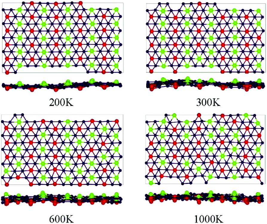 | ||
| Fig. 2 Snapshots for the equilibrium structures of BeB2 monolayer (δ phase) at the temperatures of 200 K, 300 K, 600 K, and 1000 K, at the end of 2 ps ab initio molecular dynamics simulations. The label of the atoms is the same as in Fig. 1. | ||
3.2 Electronic properties
Fig. 3 shows the band structures of the four structures that were calculated with PBE and SCAN functionals. We can see that all configurations should be metallic, and the band structures show Dirac points above the Fermi level in each case. They own unique characteristics that may allow us to modulate their electrical characteristics. The most important contributions of the density of states near the valence band maximum (VBM) come from the s orbital of Be atom and pz orbital of B atom. It suggests that the band crossing near Fermi level is due to the hybridization of s orbital and pz orbital between boron and beryllium atoms, as the origin of metallic behavior of the BeB2 monolayer. We checked the band structures by including the SOC effect. The Dirac points were opened by a tiny gap about 27 meV (α), 7 meV (β), 5 meV (γ), and 18 meV (δ), but all systems are still metallic as the SOC effect is weak in this system. Moreover, the SCAN functional was used to double check the band structures of the BeB2 monolayer, as shown by blue lines in Fig. 3. The electronic structure results are almost identical to that from PBE approach.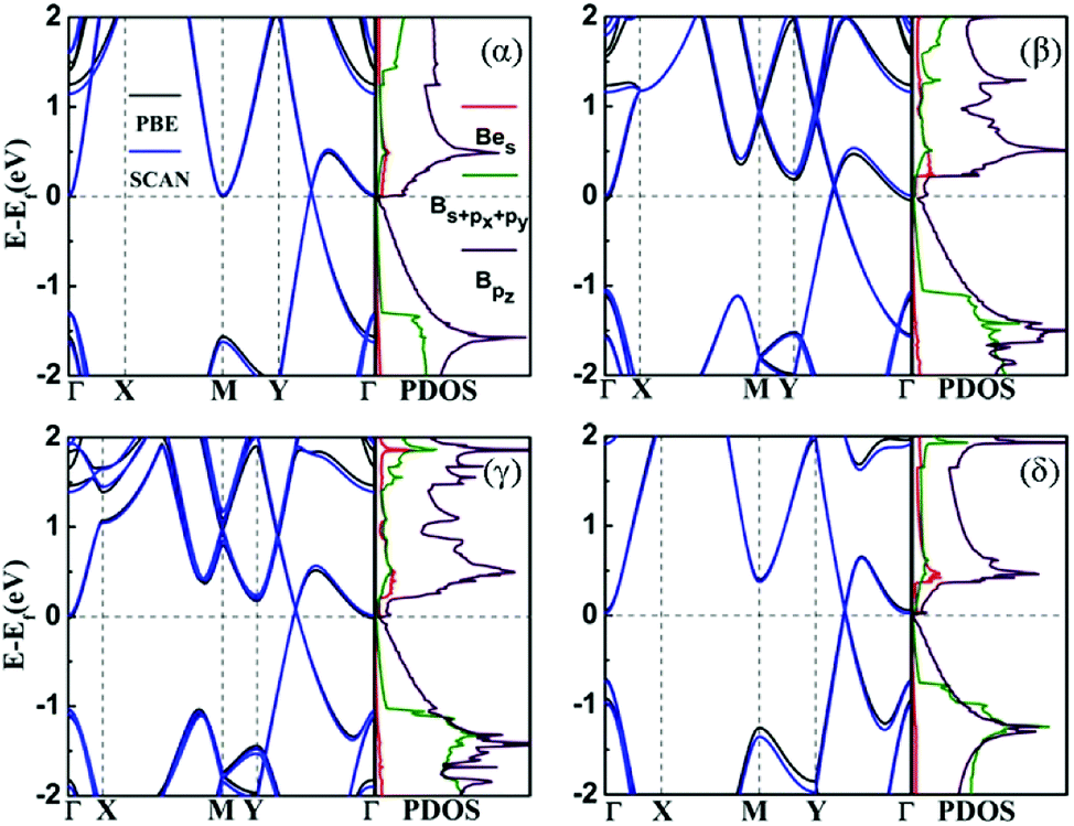 | ||
| Fig. 3 The band structures and projected density of states (PDOS) of four structures (α, β, γ, δ). The black lines in band structures and the PDOS were calculated by PBE functional, while the blue lines in band structures were calculated by SCAN functional. | ||
3.3 Strain engineering of BeB2 monolayer
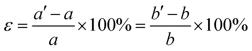
We also studied the influence of biaxial strain on the structural and electronic properties of the α, β, γ, δ monolayer structures, (α phase was reported previously by Mu et al.19 who studied the isotropic strain and uniaxial strain). The definition of biaxial strain was given by the following equation:where a′, b′ and a, b represent the lattice constants with and without applied strain respectively. The structural optimization was carried out for each specific lattice constant corresponding to a certain strain. The vertical distance h (h1, h2) of Be atom relative to the B sheet was correlated to the strain, especially in the δ phase which changed almost linearly. The compression strain will push Be atoms away from the B sheet, while the tensile strain will cause the Be atoms to approach the B sheet. In Fig. 4a, the relationship between the total energy and the strain magnitude is plotted. In the case of tensile strain, δ phase keeps the minimal energy solution from 0% to 10%. In the case of compressive strain, δ phase keeps being the minimal energy solution only under less than or equal to 6% compressive strain. When applying 7% or more compressive strain, the BeB2 sheet of β phase and γ phase strongly twist. And under such strong strain, those distorted structures show even lower energy than δ system.
 | ||
| Fig. 4 (a) The calculated total energy (eV f.u.−1) versus the biaxial strain characterized by lattice constant change (ε), with respect to the ground state of δ at zero strain. (b) The energy barriers between γ and δ phases, by artificially moving one Be atom's position (i.e. changing the middle red arrow in γ phase of Fig. 1 to green arrow) under the tensile strain ranged from 0% to 5%. (c) The separations of Dirac points from the Fermi level indicated by ΔEd of BeB2 monolayer can be tuned by the applied biaxial strain. | ||
This phenomenon indicates that the total energy of the system under compressive strain can be decreased by twisting its structure. This is not the only case in boron-based materials, for example, substrate of the flat Ag (111) can induce nanoscale undulations of borophene, which can be understood by anisotropic high bending flexibility of borophene described by a continuum model.42 More interestingly, we found a phenomenon that the Be atoms will pass through the B atomic layer in γ phase during the structure optimization under 2.5% tensile strain, namely a phase transition from γ to δ phase may take place when a tensile strain larger than 2.5% is applied. Fig. 4b indicates evidently that the energy barrier of the phase transition decreases with increasing tensile strain, which intuitively explains the mechanism that γ phase can change into δ phase. Different geometries are expected to give rise to distinct band structures, which will lead to different transport properties. The distance of Dirac point lying above Fermi level is easy to be modulated by strain (as shown in Fig. 4c). Significantly, we found a metal–semimetal transition with Dirac point lying exactly in Fermi level in α phase (under about 5% biaxial compressive strain) and δ phase (under about 3.2% and 7% biaxial tensile strain). When the strain increases, the structures return again to the normal metal state.
In Fig. 5a, we presented the three-dimensional (3D) band structure of δ phase under 3.2% biaxial tensile strain which has two Dirac cones in the first Brillouin zone locating at the Fermi level. Then we showed the band decomposed charge density of BeB2 monolayer of (Fig. 5a) at Dirac cones: the projection of the charge density of the highest valence band (Fig. 5b) and the lowest conduction band (Fig. 5c), indicating that the charge density distribution near the Fermi level exhibiting π bonding character is the physical origin of the Dirac cone. Fig. 6 presents the band structures of four structures (α, β, γ, δ) of BeB2 monolayer under biaxial strains of −10%, −5%, 5% and 10%. The Dirac cones are stable under biaxial strain ranging from −10% to 10% in α and δ phases, while they cannot maintain in β and γ phases under 10% compressive strain. Moreover, the biaxial compressive strain has more obvious modulation effect on the band structures than the biaxial tensile strain. This is corresponding to what we discussed above that the compressive strain would induce more complex structures.
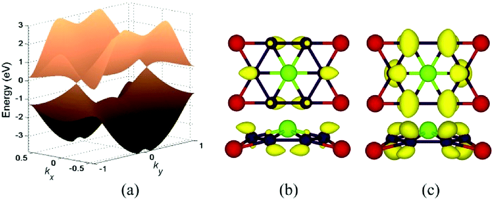 | ||
| Fig. 5 (a) The 3D band structure of δ phase under 3.2% biaxial tensile strain, which has Dirac point located at the Fermi level. Band decomposed charge density of BeB2 monolayer of (a) at Dirac point: the projection of the charge density of the highest valence band (b) and the lowest conduction band (c). The isosurface value was set at 0.21 a0−3 and 0.13 a0−3 (a0: Bohr radius) respectively. | ||
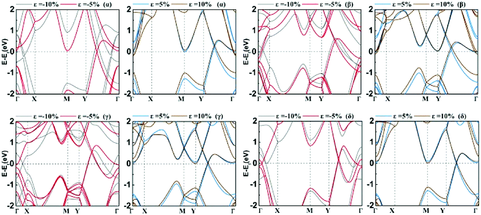 | ||
| Fig. 6 The band structures of four structures (α, β, γ, δ) of BeB2 monolayer under biaxial strains ε = −10%, −5%, 5% and 10%. | ||
4 Conclusions
In summary, three new phases (β, γ, δ) of BeB2 monolayer were proposed and discussed. Among these structures, the δ phase is the lowest energy state, as confirmed by a lower enthalpy of global searching approach. The structure of δ phase is both dynamically and thermodynamically stable as suggested by the phonon dispersions and ab initio MD simulations. All the three new structures are found to be metallic. When one Be atom crosses the B layer in the γ phase system under a tensile strain during structure optimization, one may get δ phase. We found the barrier between double wells of γ and δ phases decreases with increasing tensile strain. Interestingly, a metal–semimetal transition is found in α phase under biaxial compressive strain. Moreover, the δ phase can also have such metal–semimetal transition under biaxial tensile strain. The rich physical properties we found in the BeB2 monolayer structures will deepen our understanding of boron-based materials.Acknowledgements
This research was supported by the National Key Basic Research Program of China (Grant No. 2015CB921600), the National Natural Science Foundation of China (Grants No. 51672171, 11274222, 11547011), the QiMingXing Project (Project No. 14QA1402000) of the Shanghai Municipal Science and Technology Commission, the Eastern Scholar Program, the Shuguang Program (Grant No. 12SG34) from the Shanghai Municipal Education Commission and the fund of the State Key Laboratory of Solidification Processing in NWPU (SKLSP201703). Special Program for Applied Research on Super Computation of the NSFC Guangdong Joint Fund (the second phase) and Shanghai Supercomputer Center are also acknowledged.References
- A. J. Mannix, X.-F. Zhou, B. Kiraly, J. D. Wood, D. Alducin, B. D. Myers, X. Liu, B. L. Fisher, U. Santiago and J. R. Guest, Science, 2015, 350, 1513–1516 CrossRef CAS PubMed.
- X.-B. Li, S.-Y. Xie, H. Zheng, W. Q. Tian and H.-B. Sun, Nanoscale, 2015, 7, 18863–18871 RSC.
- C. Jin, F. Lin, K. Suenaga and S. Iijima, Phys. Rev. Lett., 2009, 102, 195505 CrossRef PubMed.
- X.-F. Zhou, X. Dong, A. R. Oganov, Q. Zhu, Y. Tian and H.-T. Wang, Phys. Rev. Lett., 2014, 112, 085502 CrossRef.
- A. H. Wasey, S. Chakrabarty, G. P. Das and C. Majumder, ACS Appl. Mater. Interfaces, 2013, 5, 10404–10408 CAS.
- L. Z. Zhang, Z. F. Wang, S. X. Du, H. J. Gao and F. Liu, Phys. Rev. B: Condens. Matter Mater. Phys., 2014, 90, 161402 CrossRef CAS.
- H. Tang and S. Ismail-Beigi, Phys. Rev. Lett., 2007, 99, 115501 CrossRef PubMed.
- G. Tai, T. Hu, Y. Zhou, X. Wang, J. Kong, T. Zeng, Y. You and Q. Wang, Angew. Chem., 2015, 127, 15693–15697 CrossRef.
- B. Feng, J. Zhang, Q. Zhong, W. Li, S. Li, H. Li, P. Cheng, S. Meng, L. Chen and K. Wu, Nat. Chem., 2016, 8, 563–568 CrossRef CAS PubMed.
- S. Xu, Y. Zhao, J. Liao, X. Yang and H. Xu, Nano Res., 2016, 9, 2616–2622 CrossRef CAS.
- J. Liu, X. Liu, X. Xu, J. Wang, C. Li, H. Wei, S. Yang, Q. Zhu, Y. Fan, X. Zhang and Z. Wang, Nanoscale Res. Lett., 2010, 5, 1340–1343 CrossRef CAS PubMed.
- A. Ramasubramaniam, D. Naveh and E. Towe, Nano Lett., 2011, 11, 1070–1075 CrossRef CAS PubMed.
- T. T. Tran, K. Bray, M. J. Ford, M. Toth and I. Aharonovich, Nat. Nanotechnol., 2016, 11, 37–41 CrossRef CAS PubMed.
- Y. G. Zhang, G. D. Cheng, W. Peng and Z. Tang, Comput. Mater. Sci., 2014, 95, 316–319 CrossRef CAS.
- Z. Qiao, W. Ren, H. Chen, L. Bellaiche, Z. Zhang, A. H. Macdonald and Q. Niu, Phys. Rev. Lett., 2014, 112, 116404 CrossRef PubMed.
- W. Ren, Z. Qiao, J. Wang, Q. Sun and H. Guo, Phys. Rev. Lett., 2006, 97, 066603 CrossRef PubMed.
- P. von Ragué Schleyer and A. I. Boldyrev, J. Chem. Soc., Chem. Commun., 1991, 1536–1538 RSC.
- H. Zhang, Y. Li, J. Hou, A. Du and Z. Chen, Nano Lett., 2016, 16, 6124–6129 CrossRef CAS PubMed.
- Y. Mu, F. Ding and H. Lu, RSC Adv., 2015, 5, 11392–11396 RSC.
- C. Lee, X. Wei, J. W. Kysar and J. Hone, Science, 2008, 321, 385–388 CrossRef CAS PubMed.
- W. Bao, F. Miao, Z. Chen, H. Zhang, W. Jang, C. Dames and C. N. Lau, Nat. Nanotechnol., 2009, 4, 562–566 CrossRef CAS PubMed.
- T. Mori, J. Mater. Sci. Lett., 2001, 20, 1857–1858 CrossRef CAS.
- M. C. Nguyen, X. Zhao, C.-Z. Wang and K.-M. Ho, RSC Adv., 2014, 4, 15061 RSC.
- P. Zhang and V. H. Crespi, Phys. Rev. Lett., 2002, 89, 056403 CrossRef PubMed.
- H. Wang, Y. Wang, J. Lv, Q. Li, L. Zhang and Y. Ma, Comput. Mater. Sci., 2016, 112, 406–415 CrossRef CAS.
- P. E. Blöchl, Phys. Rev. B: Condens. Matter Mater. Phys., 1994, 50, 17953–17979 CrossRef.
- G. Kresse and D. Joubert, Phys. Rev. B: Condens. Matter Mater. Phys., 1999, 59, 1758 CrossRef CAS.
- G. Kresse and J. Hafner, Phys. Rev. B: Condens. Matter Mater. Phys., 1993, 47, 558 CrossRef CAS.
- J. P. Perdew, K. Burke and M. Ernzerhof, Phys. Rev. Lett., 1996, 77, 3865 CrossRef CAS PubMed.
- A. Togo and I. Tanaka, Scr. Mater., 2015, 108, 1–5 CrossRef CAS.
- A. Togo, F. Oba and I. Tanaka, Phys. Rev. B: Condens. Matter Mater. Phys., 2008, 78, 134106 CrossRef.
- S. Baroni, S. De Gironcoli, A. Dal Corso and P. Giannozzi, Rev. Mod. Phys., 2001, 73, 515 CrossRef CAS.
- J. Sun, A. Ruzsinszky and J. P. Perdew, Phys. Rev. Lett., 2015, 115, 036402 CrossRef PubMed.
- R. Car, Nat. Chem., 2016, 8, 820–821 CrossRef CAS PubMed.
- J. Sun, R. C. Remsing, Y. Zhang, Z. Sun, A. Ruzsinszky, H. Peng, Z. Yang, A. Paul, U. Waghmare, X. Wu, M. L. Klein and J. P. Perdew, Nat. Chem., 2016, 8, 831–836 CrossRef CAS PubMed.
- Z.-h. Yang, H. Peng, J. Sun and J. P. Perdew, Phys. Rev. B: Condens. Matter Mater. Phys., 2016, 93, 205205 CrossRef.
- Y. Wang, J. Lv, L. Zhu and Y. Ma, Phys. Rev. B: Condens. Matter Mater. Phys., 2010, 82, 094116 CrossRef.
- H. Tang and S. Ismail-Beigi, Phys. Rev. Lett., 2007, 99, 115501 CrossRef PubMed.
- T. R. Galeev, Q. Chen, J.-C. Guo, H. Bai, C.-Q. Miao, H.-G. Lu, A. P. Sergeeva, S.-D. Li and A. I. Boldyrev, Phys. Chem. Chem. Phys., 2011, 13, 11575–11578 RSC.
- S. Cahangirov, M. Topsakal, E. Aktürk, H. Şahin and S. Ciraci, Phys. Rev. Lett., 2009, 102, 236804 CrossRef CAS PubMed.
- H. Wang, Q. Li, Y. Gao, F. Miao, X.-F. Zhou and X. G. Wan, New J. Phys., 2016, 18, 073016 CrossRef.
- Z. Zhang, A. J. Mannix, Z. Hu, B. Kiraly, N. P. Guisinger, M. C. Hersam and B. I. Yakobson, Nano Lett., 2016, 16, 6622–6627 CrossRef CAS PubMed.
Footnote |
| † Electronic supplementary information (ESI) available. See DOI: 10.1039/c7ra07137j |
| This journal is © The Royal Society of Chemistry 2017 |