
 Open Access Article
 This Open Access Article is licensed under a Creative Commons Attribution-Non Commercial 3.0 Unported Licence
Supercritical fluid electrodeposition, structural and electrical characterisation of tellurium nanowires†
Philip N. Bartlett *a,
David A. Cooka,
Mahboba M. Hasana,
Andrew L. Hectora,
Sam Marksb,
Jay Naikc,
Gillian Reida,
Jeremy Sloanb,
David C. Smithc,
Joe Spencerc and
Zondy Webberc
*a,
David A. Cooka,
Mahboba M. Hasana,
Andrew L. Hectora,
Sam Marksb,
Jay Naikc,
Gillian Reida,
Jeremy Sloanb,
David C. Smithc,
Joe Spencerc and
Zondy Webberc
aChemistry, University of Southampton, SO17 1BJ, UK. E-mail: p.n.bartlett@soton.ac.uk
bDepartment of Physics, University of Warwick, CV4 7AL, UK
cPhysics and Astronomy, University of Southampton, SO17 1BJ, UK
First published on 21st August 2017
Abstract
Supercritical fluid electrodeposition (SCFED) was employed for rapid deposition (2.5 μm min−1) of tellurium nanowires (TeNW) of nominal size range 13 nm to 55 nm diameter and tens of micrometers in length. Anodic aluminium oxide (AAO) membranes were used as hard templates for the electrodeposition by evaporation of platinum or gold onto one face to form the electrode. TeNWs were characterised both in situ and after removal of the AAO template by XRD, Raman spectroscopy and electron microscopy. The nanowires were crystalline with a strong preferred orientation in all cases. The typical 〈001〉 growth direction was always observed for samples produced using platinum coated membranes; however for the gold coated membranes, a chemical reaction between the tellurium(IV) precursor and the gold led to atypical 〈110〉 growth. Transistor devices were fabricated from individual TeNWs and their electrical properties characterised.
Introduction
Tellurium is a narrow band gap (∼0.35 eV) p-type semiconductor1 with interesting thermoelectric,2,3 photoconductive,4 piezoelectric5,6 and non-linear optical7 properties. As such, tellurium, and in particular nanostructured tellurium, may find applications in areas ranging from optoelectronics to gas sensing.8 Due to the highly anisotropic crystal structure of trigonal tellurium it has a propensity to form one-dimensional structures; tending to crystallise along the c axis.9 There is a great deal of literature where this anisotropy is exploited to form tellurium nanowires (TeNW) or nanotubes (TeNT) (a concise review is provided in the ESI†). The two most common synthetic routes are either by the chemical reduction of a soluble tellurium compound (often TeO2) frequently with hydrazine, or by solvothermal synthesis (often with addition of a reducing reagent such as hydrazine).These methods tend to form wires or rods with relatively large diameters (>100 nm) and to use solution additives, such as dodecanethiol, cetyl trimethylammonium bromide (CTAB) or poly(vinyl pyrrolidone) (PVP), as structure directing agents. In some cases these surfactants are claimed to form soft templates such as micellar/lyotropic liquid crystal phases,10,11 but typically they are present in low concentration, merely inhibiting the growth of certain Te crystal planes by adsorption.12,13 The advantage of these methods is their high yield and simplicity, however they invariably produce an untethered, disordered mass of wires or tubes. For many of the potential TeNW applications it is desirable to have structural order, which can be achieved by the use of hard templates such as mesoporous silica,14 track etched polycarbonate membranes15 or anodic aluminium oxide (AAO).16,17 Here there is no fine tuning of chemical or thermal parameters required to achieve the right nanowire dimensions and ordered arrays are formed in one step.
Electrodeposition is an attractive route to filling nanoporous templates with all sorts of conducting and semiconducting materials.18 Dense, ordered arrays of wires can be rapidly formed with their length controlled by monitoring the charge passed. However, of the 43 papers describing Te nanowires reviewed in Table S1 of the ESI,† only six report electrodeposition of Te and of these only four use porous templates as a route to TeNW formation. One of these four uses a hierarchical mesoporous silica–anodic alumina template14 and the other three use AAO templates.16,17,19 The ∼60 nm TeNWs produced in AAO by Ivanuo et al.16 were amorphous whereas those produced by Zhao et al.17 were crystalline, typically 60 nm diameter, with characteristic growth perpendicular to the (001) crystal planes. Zhao et al. also report results for optical polarization measurements for their TeNW–AAO composite. Xiang et al.19 do no report the crystallinity of their ∼27 nm TeNWs, but did demonstrate electrodeposition into micrometer scale, discretely addressable, fingers of AAO, offering the potential to fabricate single chip, multiplex nanowire devices and sensors.
One potential issue with AAO is the lack of availability of smaller pore sizes; in the three examples the pore sizes ranged from 27–60 nm on average. Keilbach et al.14 solved this problem by filing an AAO template with mesoporous silica, following the work of Wu et al.,20 to produce highly ordered pores of average diameter 10 nm. TeNWs were electrodeposited from an aqueous TeO2 solution. The one TEM result presented for the TeNWs in this mesophase system suggests that only partial filling of the pores was possible even after more than 12 hours electrodeposition.
Electrodeposition into nanoporous templates becomes more difficult with reduction in pore diameter because of problems of pore wetting caused by surface tension, slow mass transport rates down high aspect ratio pores, and pore blocking by gas evolution. Consequently, although electrodeposition into pores larger than ∼100 nm is common21 the number of successful examples in the literature significantly reduces as the pores get smaller and the number of sub 20 nm examples is very limited.22 Further, deposition into sub 20 nm pores is often slow and patchy.23
The use of supercritical fluid electrodeposition (SCFED) can overcome these problems because of the particular properties of supercritical fluids. These include the absence of surface tension, or phase separation, which allows the fluid to penetrate the smallest nanopores irrespective of chemistry of the pore wall, and low viscosity with fast rates of mass transport for solutes in supercritical fluids. The solvent properties of the fluid may be tuned by changing the pressure and temperature. In addition, it is possible to select supercritical fluids with high chemical stability and resistance to oxidation or reduction, allowing the deposition of highly reactive materials and deposition at elevated temperatures. Previously we have demonstrated the use of supercritical fluids as solvents for electrodeposition of metals and semiconductors,24,25 and Atobe et al. have reported the electrodeposition of conducting polymers into 200 nm pores in AAO.26,27 In this paper we report the first example of the electrodeposition of sub 20 nm high quality crystalline semiconducting nanowires by supercritical fluid electrodeposition.
We have shown that it is possible to electrodeposit from a range of p-block halometalates of general formula [NnBu4]x[MCly] dissolved in supercritical difluoromethane (scR32).28 In this work we use one such tellurium salt ([NnBu4]2[TeCl6]) to electrodeposit tellurium into porous AAO membranes (with pore sizes of 13, 35 and 55 nm). Rapid and complete filling of these membranes has been achieved using this highly penetrating solvent and we provide characterisation of the resulting TeNWs by XRD, STEM and EDS both within the alumina support and after removal from the membranes. Further, we demonstrate the effect of different electrode metals applied to the AAO membranes on the crystal growth direction of the TeNWs. Finally, results for resistance measurements are presented for individually contacted TeNWs.
Experimental
Chemicals
CH2F2 (R32) was purchased from Apollo Scientific Ltd (99.9%); tetrabutylammonium chloride ([NnBu4]Cl, ≥99.0%) and sodium hydroxide (≥98%) were purchased from Sigma-Aldrich Company Ltd and used without further purification. Isopropyl alcohol (IPA) was purchased from Rathburn. Tetrabutylammonium hexachlorotellurate ([NnBu4]2[TeCl6]) was prepared by the method described previously.29All reagents were handled under rigorously anhydrous conditions under a dry dinitrogen atmosphere and by using standard Schlenk and glove box techniques.
Preparation of AAO membranes for electrodeposition
Membranes, with a range of pore diameters, were purchased from Synkera Technologies Inc. as either 1 × 1 cm squares or 13 mm diameter discs. All membranes were unsupported with the pores open at both faces. Pores were nominally 13 ± 2 nm diameter (membrane thickness 51 ± 1 μm and pore density 1 × 1011 cm−2), 35 ± 3 nm diameter (membrane thickness 48 ± 1 μm and pore density 1 × 1010 cm−2), or 55 ± 5 nm diameter (membrane thickness 50 ± 2 μm and pore density 1 × 109 cm−2).AAO membranes were first coated with a thin chromium adhesion layer (5–10 nm) by evaporation. The electrode metal was then evaporated to a thickness of approximately 200 nm (Leybold Lab 700 e-beam evaporator). After metal coating, the membranes were divided into smaller sections (typically 0.22 to 0.24 cm2) and contacted (silver epoxy resin: CircuitWorks®) to steel wires of 0.5 mm diameter that were insulated with 1/16′′ polyether etherketone (PEEK) tubing. The contact, steel and metal coated face of the membrane were then insulated by coating with epoxy resin (Struers EpoFix).
Supercritical fluid electrochemistry
Cyclic voltammetry (CV) and chronoamperometry (CA) were performed with an Autolab PGSTAT302 potentiostat (Metrohm) using a standard 3 electrode configuration with a 0.5 mm Pt disc quasi reference electrode (the Pt quasi reference was used to avoid contamination of the Te nanowires, its potential is ca. −0.14 V vs. DMFc/DMFc+,30 DMFc is decamethylferrocene) and Pt grid counter electrode. Working electrodes were Pt or Au coated AAO membranes or polished platinum discs of 0.5 mm or 30 μm diameter. The electrodes were sealed into the high pressure electrochemistry cell (described elsewhere31) using PEEK tubing insulation and 2 piece nut and ferrule compression fittings. [NnBu4]2[TeCl6] and [NnBu4]2Cl were transferred into the cell inside a nitrogen-purged glove box (Belle Technology). Once loaded, the cell was sealed and transferred to a high pressure line, where it was heated to the operating temperature of 86 °C before introducing the R32 using a Jasco PU-1580-CO2 pump. The final solution pressure during experiments was 172 (±1) bar.Freeing TeNWs from AAO membrane
When required the alumina membranes were dissolved by immersing in 4 M NaOH leaving the nanowires still contacted to the residual metal film. These were then washed with deionised water and HPLC grade IPA. TeNWs could then be imaged at this stage as bundles attached to the metal film or could be dispersed into IPA by sonication and then drop cast onto substrates for electrical measurements or 3.05 mm copper grids with lacy carbon support film (Agar Scientific) for TEM/STEM imaging.Raman measurements
Raman spectra were measured on contacted and uncontacted TeNWs on substrates which had been prepared for electrical characterisation; i.e. uncontacted TeNWs that had been exposed to the same processes, but were away from the metal contacts. Individual TeNWs were located and imaged by a white light microscope built into the Raman system32 which allows the laser excitation spot to be positioned onto the nanowire with a precision of 1 μm. The excitation source was a Coherent MIRA-900p titanium:sapphire laser source in continuous-wave mode set to 702 nm incident wavelength (1.766 eV) and filtered using a PhotonETC TLS 820 laser line filter. Raman spectra were taken in a back-scattering geometry using an Olympus LMPan IR 50× objective to focus the excitation beam onto the sample to produce a 2 μm diameter spot with an excitation intensity of 0.6 μW μm−2. The back scattered light was collected and focused into a Princeton Instruments TriVista triple 600 nm spectrometer, configured in subtractive mode, using 900, 900 and 1800 lines mm−1 gratings in the three stages. The spectra were measured on a Princeton Instruments, deep depleted, liquid N2 cooled silicon CCD. Measurements were made at room temperature with the sample exposed to the ambient atmosphere and their dependence on excitation and scattered polarisation determined.X-ray diffraction
X-ray diffraction (XRD) patterns were collected in parallel beam θ–2θ geometry using Cu-Kα radiation with a Rigaku Smartlab Thin Film diffractometer with a DTex 250 1D detector. Phase matching and lattice parameter refinements used the Rigaku PDXL2 package and standard patterns from ICSD. Pole figure measurements used the in-plane pole figure geometry.Electron microscopy
Imaging was undertaken using a JEOL ARM 200F operating at 200 kV with a Schottky emitter. TEM and STEM analysis was undertaken with probe and image CEOS correction. TEM data were recorded on an unshuttered Gatan Orius SC1000 CCD camera and ADF STEM images obtained using a JEOL annular field detector. EDX maps were acquired using an Oxford Instruments 100 mm2 windowless energy-dispersive X-ray detector and Aztec software.Thin sections of the AAO/TeNW composite were prepared using conventional focused ion beam milling (FIB) and lift out techniques.33 FIB cross sections were prepared using a JEOL 4500FIB/SEM operating with a 30 kV LaB6 electron gun and 30 kV Ga+ ion source.
Electrical characterization of TeNWs
In order to enable electrical characterisation of the deposited nanowires, transistor structures were manufactured using standard microfabrication techniques. Freed nanowires were drop cast onto specially prepared 1 cm squares of 100 nm thick silicon oxide coated N〈100〉P silicon wafers with resistivity 1–10 Ω cm−1 (IDB Technologies Ltd.). Four point contacts to individual nanowires were made Ni, Cr/Au or W by either e-beam lithography and lift-off (Ni or Cr/Au) or e-beam induced deposition (W and C). Full details of the various steps in the device preparation are presented in the ESI.†The electrical characterisation of the nanowire transistor devices was performed using a Cascade M150 probe station and a MSA-400 Micro System Analyser with the device in the dark and at room temperature. Each sample was characterised to determine the pairwise resistances between all of the electrodes and the leakage behaviour between the electrodes and the silicon back gate. Any devices with significant defects were then discarded. Finally, the gate dependent 4 point resistance of each nanowire was measured as a function of gate voltage. For some samples the combination of high channel resistance and bond pad capacitance meant that charging times were long, i.e. on the scale of seconds, and so care was taken to ensure that the measurement time was sufficiently long that it had no effect on the final results.
Results
Voltammetry
Previously we reported the voltammetry of the tellurium complex in scR32 at a gold disc working electrode28 and this was complicated slightly by a reaction between the Te(IV) species and the gold. Here platinum electrodes were used to avoid such complications. The electrochemistry of the tellurium complex was first investigated by cyclic voltammetry (Fig. 2a–c). Using the method described previously,31 microdisc voltammetry in different tellurium concentrations was used to estimate the solubility limit as 1.7 mM. The voltammograms at the platinum disc electrodes shown in Fig. 2a and b were recorded in solution concentrations lower than this limit, but for deposition experiments a saturated solution was used.It is common for Te(IV) species to reduce to tellurium in a single, 4e− step in aprotic solvents34,35 and for each working electrode used here we see a single reduction wave with an onset potential of around −0.2 V vs. Pt. Typically the mass transport controlled current in scR32 is very erratic due to the low viscosity and high thermal convection in the supercritical fluid; in Fig. 1a only small variations in the cathodic wave are observed at cathodic potential and this is due to the use of a short plastic baffle fitted to the end of the electrode. This baffle significantly reduces the effects of convection at the macroelectrode. In the case of the microelectrode (Fig. 1b) no baffle was needed as the thickness of the diffusion layer of such a disc is much smaller (<100 μm hemisphere) and is scarcely affected by the turbulence in the solution. This cathodic wave is due to the 4e− reduction of Te(IV) to Te(0) at the platinum surface. This was confirmed by analysis of the solid deposit formed by holding the potential at various values along the wave.
 | ||
| Fig. 1 (A–C) Cyclic voltammetry in 1 mM [NnBu4]2[TeCl6] with 50 mM [NnBu4]Cl supporting electrolyte in scR32 at 86 °C and 172 bar. Working electrodes were swept from 0 V at 100 mV s−1 (direction of scan indicated by arrows). CE = Pt grid, RE = 0.5 mm Pt disc and WE = (A) 0.5 mm Ø Pt disc, (B) 30 μm Ø Pt disc, (C) 0.2 cm2 AAO membrane (nominally 13 nm Ø pores) coated with Pt film. (D) 0.25 cm2 AAO membrane (nominally 13 nm Ø pores) coated with Pt film held at −1.0 V (charge passed = 0.536 C). | ||
The diffusion coefficient of the Te(IV) species was estimated from the plateau of the cathodic wave (Fig. 1b) using
| iL = 4nFDca | (1) |
The charge under the stripping peak (centred at 0.29 V and 0.11 V for the macro and microdiscs respectively) is consistently 50% of the charge passed during the cathodic plating wave which suggests that the tellurium is re-oxidised to a soluble Te(II) species. There is also a shoulder to this peak (anodic of the current maximum) that we attribute to a 2nd phase of tellurium deposit. Indeed, it was observed in SEM images that the tellurium first forms a compact layer of small crystallites near the electrode surface and then the tellurium continues to grow on top of this as filaments.
The electrodes used to deposit the TeNWs were AAO membranes, sputtered on one side with a platinum film. In the case of these porous membrane electrodes (Fig. 1c) the main stripping peak at 0.13 V is accompanied by a second at 0.38 V. In this case, the solution near the surface of the platinum is stagnant and the stripping of Te may be hindered slightly by the solubility of Te(II) and this could be why we see a slightly lower stripping efficiency of 41.5% here. On the other hand, the quiescent nature of the solution in the pores means that (unlike the polished electrodes in the bulk solution) the Te(II) lingers long enough near the electrode to be oxidised further to Te(IV) and this is the process occurring during the 2nd anodic peak.
Electrodeposition of TeNWs
TeNWs were electrodeposited into AAO membranes with nominal pore sizes of 13 nm, 35 nm and 55 nm. The electrode potential was fixed at −1.0 V and the current transient recorded. Fig. 1d shows the chronoamperometric response for a typical deposition experiment. The initial current drops sharply as the Te(IV) is depleted at the Pt surface. Once the diffusion profile is established the current slowly creeps up. We believe this is because the transport rate is fixed by the length of the pore, but as the TeNWs grow the effective pore length decreases and so the current increases.The current gradient increases after a time due to the tellurium completely filling the pores and overgrowing on the membrane surface. For 13 nm pores (as in Fig. 1d) this typically occurs at around 1200 s; using this inflection in current we are able to estimate the rate of deposition as 2.5 μm min−1. This is fast compared to deposition into AAO from aqueous solvents. Ivanou et al.16 reported deposition of Te into 60 nm diameter AAO pores from 1 mM TeO2 in 0.1 M HNO3 and from their publication it is possible to estimate a deposition rate of approximately 0.031 μm min−1.
The nature of the current inflection was investigated by stopping the deposition experiment at times before and after this feature and analysing the membrane surface by SEM. If the deposition is stopped prior to the inflection then the membrane surface is clean and the pores are still visible; however if the deposition is stopped after, then Te deposits are visible on the surface.
Raman measurements on TeNWs
Representative Raman spectra obtained from an uncontacted and a contacted Te nanowire are shown in Fig. 2 with additional spectra given in the ESI.† In both cases presented in Fig. 2 the spectra were obtained with incoming and scattered polarisation parallel to the nanowire direction observed using the microscope built into the Raman system. No significant Raman scattering was obtained when incoming or scattered polarisations were perpendicular to the nanowire. The Raman spectrum of the uncontacted nanowire shows three clear features that are characteristic of elemental Te,37 together with a small peak due to the silicon substrate,38 but none of the peaks characteristic of tellurium oxides.39 Fitting both spectra to Lorentzian line shapes yielded a centre Raman shift of 96.5 cm−1 for the 1st ETO/LO mode, 126.5 cm−1 for the A1 mode and 145 cm−1 for the 2nd ETO/LO mode in the isolated nanowire. In the contacted nanowire, only the A1 mode was observable and was centred at 123.5 cm−1. In both samples the uncertainty to the fitted shifts was +/−0.4 cm−1, based on the pixel resolution of the spectrometer. The mode labelled at ∼303 cm−1 seen in both spectra corresponds to a second-order Raman peak of the silicon substrate. Whilst in principle the Raman spectrum observed should depend on the growth direction of the Te, the small differences between the various options,37 and the possibility of shifts due to confinement and strain mean that we cannot separately confirm the growth direction using the Raman spectrum. The Raman spectrum from the contacted nanowire shows a single peak at the same shift as the main Te Raman peak, which is significantly suppressed compared with the uncontacted nanowire. This spectrum confirms that the Te nanowire has survived the contacting process. The reduction in scattering efficiency is greater than the fraction of the wire which is obscured by the metal contacts, however as the separation of the contacts (∼750 nm) is comparable with the wavelength of the radiation, near field effects could easily account for the additional suppression.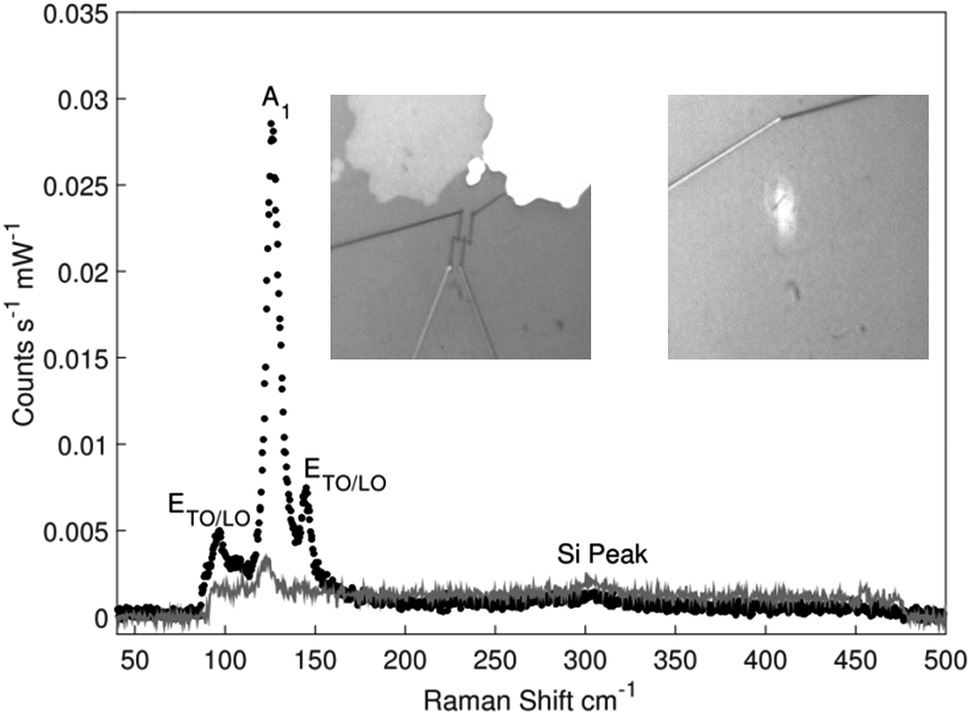 | ||
| Fig. 2 Representative Raman spectra of an isolated Te nanowire (black circles) and a Cr/Au contacted Te nanowire (grey line). In both cases the input/collection polarisation was set parallel to the orientation of the nanowire on the substrate. The insets show optical microscope images of the contacted TeNW (left) and the isolated TeNW (right) used. | ||
X-ray diffraction results
X-ray diffraction patterns of tellurium samples deposited into anodic alumina membranes were collected in a symmetric θ–2θ geometry with the membrane flat, to maximise penetration of the X-rays into the membrane. Tellurium was found in all cases after deposition. Strong preferred orientation was observed, with 〈001〉 texture (Fig. 3). | ||
| Fig. 3 (A) The XRD patterns of Te wires deposited into 13 nm pores in AAO membranes showing the two different orientations. Refined lattice parameters were a = 4.469(12) and c = 5.84(3) Å in the 〈110〉 sample, and a = 4.436(15) and c = 5.923(16) Å in the 〈001〉 sample. The top pattern shows a standard literature pattern for tellurium in P3121 with a = 4.458(3) and c = 5.925(1) Å.40 (B) The crystal structure of Te showing the spiral chains of atoms along the [001] axis.40 | ||
It is worth noting that preliminary TeNW deposition experiments were conducted with gold coated AAO membranes. Once again, strong preferred orientation was observed, but here the reaction of the Te(IV) species with the gold interface had a significant influence on the crystal orientation of the deposited TeNWs. The typical 〈001〉 texture could be observed only if the AAO membrane electrode was polarised immediately upon introducing the electrolyte to the cell. Where the fluid was left in contact with the gold-backed membrane for a period before deposition, the TeNWs grew with a strong 〈110〉 orientation (Fig. 3). These orientation effects were observed in 13, 35 and 55 nm pore sizes.
The symmetric geometry maintains the diffraction vector at the membrane surface normal, and hence the observed texture is consistent with growth of the nanowires along the [110] or [001] crystallographic axis. Pole figure studies (Fig. 4) confirmed growth along these axes with fibre texture, i.e. all wires within a sample grow along the same axis but there is rotational freedom in the plane of the membrane. For the TeNWs grown in Pt backed AAO the 〈003〉 pole figure (Fig. 4a) shows a strong surface normal peak suggesting this is the main axis of the Te wires. In the Te crystal structure the angle between the [001] and [111] axes is 69.4°, so 〈001〉 fibre texture should result in a ring in the 〈111〉 pole figure with radius of 69.4° around the surface normal (the diffuse ring that is seen). For the TeNWs grown in Au backed AAO where the fluid was left in contact with the gold-backed membrane for a period before deposition the 〈110〉 pole figure (Fig. 4b) shows a strong, sharp surface normal peak suggesting this is the main axis of the Te wires. In the Te crystal structure the angle between the [110] and [111] axes is 21.6°, so 〈110〉 fibre texture should result in a ring in the 〈111〉 pole figure with radius of 21.6° around the surface normal (the small sharp ring that is seen).
 | ||
| Fig. 4 Pole figure measurements on Te wires deposited into 13 nm pores. (A) Wires deposited on Pt coated AAO membranes, in which the symmetric scan (Fig. 3) showed 〈001〉 texture. (B) Wires deposited in Au coated AAO membranes, where the fluid was left in contact with the gold-backed membrane for a period before deposition, for which the symmetric scan (Fig. 3) showed 〈110〉 texture. | ||
Electron microscopy of TeNWs
After removal of the anodic alumina template with NaOH, the TeNWs were first imaged while still in contact with the evaporated metal film (Fig. 5a). Unsupported, the wires lay on the metal substrate in long bundles looking something like cooked spaghetti. EDX measurements of these bundles confirmed them to be pure Te and while it is possible to see that they are continuous over tens of micrometers in length, it is not possible to assess their crystallinity or precise dimensions at this resolution. Therefore, samples of these wires were suspended in isopropyl alcohol and dropped onto TEM grids for high resolution imaging. Thin sections were also removed by FIB milling in order to analyse the TeNWs inside the templates. | ||
| Fig. 5 (A) Bundles of TeNWs still attached to the gold substrate after dissolving the 13 nm AAO membrane in NaOH imaged using a JEOL-JSM 6500F microscope (the wires were confirmed to be Te by EDX). (B) Composite image of thin section of TeNWs inside AAO membrane (nominally 35 nm Ø pores) including EDX mapping. (C) STEM image of an individual “13 nm” TeNW, with SAXD pattern inserted. | ||
Crystalline Te nanowires were directly observed in both the 13 nm and 55 nm diameter membranes (Fig. 5b). The images show gold at the bottom of the pores in the case of the gold coated AAO membranes (Fig. 5b). The nanowires grown on Pt backed AAO were found to have a uniform growth orientation parallel to the 〈001〉 axis, shown in Fig. 5c, left panel, which was independent of the nanowire diameter. EDX analyses of the nanowires show no contaminants within the bulk of the nanowire, but does highlight the amorphous alumina coating on the nanowires, remnant from the membrane. The TEM images show that the (nominally) “13 nm” membranes produce nanowires with a diameter range typically between 10 and 20 nm with some diameter constrictions around 7 nm. The “55 nm” membrane nanowires have a much wider range with nanowire diameters, typically between 50 and 80 nm, but with some outliers and diameter constrictions of 30 nm and greater than 90 nm. The volume filling of the AAO template is excellent and this is the cause of the variations in wire diameters observed in the TEM images; as the AAO pores are never perfectly straight or uniform in diameter.
Electrical characterization of individual TeNWs
19 devices covering a range of nanowire diameters and contact metals were studied (for details see ESI†). The zero gate voltage four point resistances of the devices varied by over three orders of magnitude from around 10 MΩ to around 10 GΩ with the majority of devices (13 of the 19) having a four point resistance greater than 1 GΩ. There was no clear dependence of the device resistance on nanowire diameter or contact metal.The gate dependence of the four point resistance of the transistors was measured for all 19 devices. In general, these were often noisy with the best results obtained on low resistance devices. In each case there was a small increase in the conductance of the device for negative gate potentials consistent with p-type behaviour and in agreement with results in the literature although the on/off ratios for our devices were much smaller than for some of the previously published results for TeNWs prepared by hydrothermal synthesis.41,42
Conclusions
Crystalline TeNWs of varying diameters, including down to ca. 10 nm, were readily prepared by electrodeposition from supercritical R32 using metal coated AAO membranes as templates. Tellurium reduction proceeds under potentiostatic control, completely filling the AAO pores without voids and accurately replicating the shape of the template. The diameter of the TeNWs produced here is comparable to the smallest reported in the literature, but with the advantage of rapid deposition rate (2.5 μm min−1) and precise control of wire length. This represents the first example of semiconductor nanowires fabricated using the SCFED technique. There is a strong alignment of the crystal planes in these wires that is influenced by the choice of electrode metal used to coat the AAO membrane. For Pt coated AAO the TeNWs have strong 〈001〉 alignment however for Au coated AAO the alignment changes to 〈110〉 if the electrolyte is left in contact with the Au coated template for some time. Individual Te nanowires were successfully contacted for electrical characterization and showed p-type behaviour with high resistances.Based on the high pore penetration and fast diffusion rates inherent to the supercritical fluid, it is reasonable to expect that the SFCED technique will enable production of even more extreme TeNW dimensions.
Conflicts of interest
There are no conflicts of interest to declare.Acknowledgements
This work is part of the Supercritical Fluid Electrodeposition project, a multi-disciplinary collaboration of British universities investigating the fundamental and applied aspects of SCFs funded by a Programme grant from the EPSRC (EP/I013394/1). The authors also thank EPSRC for funding the Smartlab diffractometer under EP/K00509X/1 and EP/K009877/1. PNB gratefully acknowledges receipt of a Wolfson Research Merit Award.Notes and references
- H. G. Junginger, Solid State Commun., 1967, 5, 509–511 CrossRef CAS.
- S. Q. Lin, W. Li, Z. W. Chen, J. W. Shen, B. H. Ge and Y. Z. Pei, Nat. Commun., 2016, 7, 10287 CrossRef CAS PubMed.
- V. D. Das, N. Jayaprakash and N. Soundararajan, J. Mater. Sci., 1981, 16, 3331–3334 CrossRef CAS.
- H. H. Li, P. Zhang, C. L. Liang, J. Yang, M. Zhou, X. H. Lu and G. A. Hope, Cryst. Res. Technol., 2012, 47, 1069–1074 CrossRef CAS.
- D.-B. Jeong, J.-H. Lim, J. Lee, H. Park, M. Zhang, Y.-I. Lee, Y.-H. Choa and N. V. Myung, Electrochim. Acta, 2013, 111, 200–205 CrossRef CAS.
- T. I. Lee, S. Lee, E. Lee, S. Sohn, Y. Lee, S. Lee, G. Moon, D. Kim, Y. S. Kim, J. M. Myoung and Z. L. Wang, Adv. Mater., 2013, 25, 2920–2925 CrossRef CAS PubMed.
- H. M. Isomaki and J. Vonboehm, Phys. Scr., 1982, 25, 801–803 CrossRef CAS.
- W. Zhenghua, W. Lingling, H. Jiarui, W. Hui, P. Ling and W. Xianwen, J. Mater. Chem., 2010, 20, 2457–2463 RSC.
- W. C. Cooper, Tellurium, Van Nostrand Reinhold Co., New York, 1971 Search PubMed.
- B. Xi, S. Xiong, H. Fan, X. Wang and Y. Qian, Cryst. Growth Des., 2007, 7, 1185–1191 CAS.
- G. Xi, Y. Liu, X. Wang, X. Liu, Y. Peng and Y. Qian, Cryst. Growth Des., 2006, 6, 2567–2570 CAS.
- Z. P. Liu, Z. K. Hu, Q. Xie, B. J. Yang, J. Wu and Y. T. Qian, J. Mater. Chem., 2003, 13, 159–162 RSC.
- G. S. Cao, X. J. Zhang, L. Su and Y. Y. Ruan, J. Exp. Nanosci., 2011, 6, 121–126 CrossRef CAS.
- A. Keilbach, J. Moses, R. Koehn, M. Doeblinger and T. Bein, Chem. Mater., 2010, 22, 5430–5436 CrossRef CAS.
- C. Frantz, N. Stein, Y. Zhang, E. Bouzy, O. Picht, M. E. Toimil-Molares and C. Boulanger, Electrochim. Acta, 2012, 69, 30–37 CrossRef CAS.
- D. K. Ivanou, Y. A. Ivanova, A. D. Lisenkov, M. L. Zheludkevich and E. A. Streltsov, Electrochim. Acta, 2012, 77, 65–70 CrossRef CAS.
- A. Zhao, L. Zhang, Y. Pang and C. Ye, Appl. Phys. A: Mater. Sci. Process., 2005, 80, 1725–1728 CrossRef CAS.
- W. Ahmed and N. Ali, Manufacturing nanostructures, One Central Press (OCP), 2014 Search PubMed.
- Y. Xiang, A. Keilbach, L. M. Codinachs, K. Nielsch, G. Abstreiter, A. Fontcuberta i Morral and T. Bein, Nano Lett., 2010, 10, 1341–1346 CrossRef CAS PubMed.
- Y. Y. Wu, G. S. Cheng, K. Katsov, S. W. Sides, J. F. Wang, J. Tang, G. H. Fredrickson, M. Moskovits and G. D. Stucky, Nat. Mater., 2004, 3, 816–822 CrossRef CAS PubMed.
- X.-J. Wu, F. Zhu, C. Mu, Y. Liang, L. Xu, Q. Chen, R. Chen and D. Xu, Coord. Chem. Rev., 2010, 254, 1135–1150 CrossRef CAS.
- T. R. Kline, M. Tian, J. Wang, A. Sen, W. H. M. Chan and T. E. Mallouk, Inorg. Chem., 2006, 45, 7555–7565 CrossRef CAS PubMed.
- M. Arefpour, M. Almasi Kashi, A. Ramazani and A. H. Montazer, Nanotechnology, 2016, 27, 275605 CrossRef CAS PubMed.
- P. N. Bartlett, D. A. Cook, M. W. George, A. L. Hector, J. Ke, W. Levason, G. Reid, D. C. Smith and W. Zhang, Phys. Chem. Chem. Phys., 2014, 16, 9202–9219 RSC.
- J. Ke, W. T. Su, S. M. Howdle, M. W. George, D. Cook, M. Perdjon-Abel, P. N. Bartlett, W. J. Zhang, F. Cheng, W. Levason, G. Reid, J. Hyde, J. Wilson, D. C. Smith, K. Mallik and P. Sazio, Proc. Natl. Acad. Sci. U. S. A., 2009, 106, 14768–14772 CrossRef CAS PubMed.
- M. Atobe, S. Iizuka, T. Fuchigami and H. Yamamoto, Chem. Lett., 2007, 36, 1448–1449 CrossRef CAS.
- M. Atobe, N. Yoshida, K. Sakamoto, K. Sugino and T. Fuchigami, Electrochim. Acta, 2013, 87, 409–415 CrossRef CAS.
- P. N. Bartlett, J. Burt, D. A. Cook, C. Y. Cummings, M. W. George, A. L. Hector, M. M. Hasan, J. Ke, W. Levason, D. Pugh, G. Reid, P. W. Richardson, D. C. Smith, J. Spencer, N. Suleiman and W. Zhang, Chem.–Eur. J., 2016, 22, 302–309 CrossRef CAS PubMed.
- P. N. Bartlett, D. Cook, C. H. de Groot, A. L. Hector, R. Huang, A. Jolleys, G. P. Kissling, W. Levason, S. J. Pearce and G. Reid, RSC Adv., 2013, 3, 15645–15654 RSC.
- C. Y. Cummings, J. A. Branch, P. W. Richardson and P. N. Bartlett, Electrochim. Acta, 2016, 187, 323–328 CrossRef CAS.
- D. Cook, P. N. Bartlett, W. Zhang, W. Levason, G. Reid, J. Ke, W. Su, M. W. George, J. Wilson, D. Smith, K. Mallik, E. Barrett and P. Sazio, Phys. Chem. Chem. Phys., 2010, 12, 11744–11752 RSC.
- D. C. Smith, J. H. Spencer, J. Sloan, L. P. McDonnell, H. Trewhitt, R. J. Kashtiban and E. Faulques, J. Visualized Exp., 2016, e53434, DOI:10.3791/53434.
- L. A. Giannuzzi and F. A. Stevie, Micron, 1999, 30, 197–204 CrossRef.
- O. I. Kuntyi, E. V. Okhremchuk and V. T. Yavorskii, Russ. J. Appl. Chem., 2007, 80, 1327–1330 CrossRef CAS.
- Y. Liftman, M. Albeck, J. M. E. Goldschmidt and C. Yarnitsky, Electrochim. Acta, 1984, 29, 1673–1678 CrossRef CAS.
- P. N. Bartlett and J. Branch, J. Electroanal. Chem., 2016, 780, 282–289 CrossRef CAS.
- A. S. Pine and G. Dresselhaus, Phys. Rev. B: Solid State, 1971, 4, 356 CrossRef.
- P. A. Temple and C. E. Hathaway, Phys. Rev. B: Solid State, 1973, 7, 3685–3697 CrossRef CAS.
- J. C. Champarnaud-Mesjard, S. Blanchandin, P. Thomas, A. Mirgorodsky, T. Merle-Mejean and B. Frit, J. Phys. Chem. Solids, 2000, 61, 1499–1507 CrossRef CAS.
- N. Bouad, L. Chapon, R. M. Marin-Ayral, F. Bouree-Vigneron and J. C. Tedenac, J. Solid State Chem., 2003, 173, 189–195 CrossRef CAS.
- L. Lin-Bao, L. Feng-Xi, H. Xiao-Li, Y. Tian-Xin, H. Ji-Gang, Y. Yong-Qiang, W. Chun-Yan, W. Li, Z. Zhi-Feng, L. Qiang and J. Jian-Sheng, J. Nanopart. Res., 2012, 14, 967–969 CrossRef.
- F. Liang and H. Qian, Mater. Chem. Phys., 2009, 113, 523–526 CrossRef CAS.
Footnote |
| † Electronic supplementary information (ESI) available: Table of TeNW papers, experimental details, characterization results. See DOI: 10.1039/c7ra07092f |
| This journal is © The Royal Society of Chemistry 2017 |