
 Open Access Article
 This Open Access Article is licensed under a Creative Commons Attribution-Non Commercial 3.0 Unported Licence
Band gap opening of graphene by forming a graphene/PtSe2 van der Waals heterojunction†
Zhaoyong Guan *ab,
Shuang Nic and
Shuanglin Hu*a
*ab,
Shuang Nic and
Shuanglin Hu*a
aInstitute of Nuclear Physics and Chemistry, China Academy of Engineering Physics, Mianyang, Sichuan 621900, P. R. China. E-mail: guanzhaoyong@gmail.com; hushuanglin@caep.cn
bDepartment of Physics, State Key Laboratory of Low-Dimensional Quantum Physics, Tsinghua University, Beijing 100084, P. R. China
cResearch Center of Laser Fusion, China Academy of Engineering Physics, Mianyang, Sichuan 621900, P. R. China
First published on 22nd September 2017
Abstract
Opening a band gap and finding a suitable substrate for graphene are two challenges for constructing graphene based nano-electronic devices. Recently, a new two-dimensional layered crystal PtSe2 with novel electronic properties has been efficiently synthesized by direct “selenization”. In this work, we demonstrate that PtSe2 can be used as a suitable substrate for graphene by forming a graphene/PtSe2 van der Waals (vdW) heterojunction. Hybrid density functional calculations show that PtSe2 as a substrate could introduce a sizeable gap of 0.264 eV into graphene, which is sufficiently large enough for overcoming the thermal excitation of electrons at room temperature. The underlying mechanism for the band gap opening of graphene is that the PtSe2 substrate can produce inhomogeneous electrostatic potential to break the symmetry of the A and B sub-lattices of graphene. By applying a vertical strain to the graphene/PtSe2 vdW heterojunction, the electronic properties of the heterojunction can be effectively tuned. As the vertical strain increases, the band gap monotonously increases and can reach as large as 0.781 eV. The tunable band gap, together with the high carrier mobility of both graphene and PtSe2, suggests the great potential of the PtSe2/graphene heterojunction in high performance field effect transistors.
1 Introduction
Graphene, a single layer of carbon atoms arranged in a two-dimensional (2D) honeycomb lattice,1 has attracted considerable attention for its wide range of extraordinary properties,2–6 including fantastic electronic properties, 2.3% absorption in the white light spectrum, high specific surface area, high Young’s modulus, excellent thermal conductivity and so on. One of the most interesting characteristics of graphene is the massless low-energy excitations, Dirac fermions.7 Compared with ordinary electrons, Dirac fermions behave in an unusual way when subjected to a magnetic field, leading to new physical phenomena, such as the quantum Hall effect (QHE).7,8Unfortunately, the lack of a finite band gap in graphene implies that the current can never be tuned off completely, which is a major obstacle for using graphene in logic and high speed switching devices.9,10 The methods of opening the band gap of graphene11–21 include cutting the graphene into many kinds of chiral nano-ribbon, rolling the graphene into single-wall nanotubes,11,12 chemical functionalization and strain engineering.17 In addition, applying an external electric field to a bilayer graphene could also open a band gap,18–20 but the field strength required is too strong to be realized and controlled in the experiments.9,18,21
On the other hand, for graphene based electronic devices, the hybrid graphene/substrate vdW heterojunctions are easy to be fabricated, and the electronic properties of the graphene could be tuned by the substrate.22–37 Moreover, some excellent intrinsic characteristics such as high carrier mobility could be effectively preserved.22–30,33–36 So it is quite necessary to find out the proper substrate for graphene.22 In experiments, the most commonly used substrates are SiC23–25 and SiO2,26, metals such as Cu27 and Ni28, and semiconducting MoS2,29 but they may not be the ideal substrates because of surface roughness or the smaller opening band gaps of graphene when using them. For example, it was predicted that MoS2 could open quite a small band gap.30,31 Although SiC and SiO2 are widely adopted, their surfaces are too rough.23–26
In early work, g-C3N4 was proposed as a suitable substrate by forming a graphene/g-C3N4 vdW heterojunction,32 but g-C3N4 opened the band gap of the graphene as small as 0.07 eV. Graphite was also used as the substrate in experiment, but it could only open the band gap at about 0.03 eV,33 which suggests a probable low on/off ratio for graphene. Compared with the above mentioned substrates, hexagonal boron nitride (h-BN) with a rather smooth surface showed a small lattice mismatch with graphene.34,35 However, the electronic properties of the graphene/h-BN vdW heterojunction strongly depend on its stacking order, which cannot be easily controlled experimentally.34–37
Very recently, a PtSe2 monolayer has been successfully synthesized through an epitaxial growth on a Pt substrate by direct “selenization”.38–40 In the unit cell of PtSe2, two Se atoms are related to each other by inversion symmetry, and one Pt atom layer is sandwiched between two Se layers, with the space group P3m1. The PtSe2 monolayer is an indirect semiconductor with a band gap of 1.96 eV. Bulk PtSe2 has shown great potential in gas sensors,39,40 high powered electronic devices (such as field-effect transistors (FETs)) with high electron mobility,39,41,42 electrocatalysis,43 spin-layer locking materials,44 and type-II Dirac fermion materials.45 The carrier mobility of graphene is as high as 2.0 × 105 cm2 V−1 s−1,2,3 and the value for PtSe2 is 210 cm2 V−1 s−1, which is comparable to that of MoS2.41,42 From this point, both graphene and PtSe2 are suitable for constructing FETs. So it is interesting to know: (i) can PtSe2 be used as a substrate to open a large band gap of graphene for a high on/off ratio? (ii) Can the electronic properties of the formed graphene/PtSe2 vdW heterojunction be modulated by changing the interlayer interaction?
In this article, using a first-principles method with long-range dispersion correction,46,47 we calculated the structural and electronic properties of the graphene/PtSe2 vdW heterojunction. We found that PtSe2 can open the band gap of graphene to be as large as 0.264 eV (calculated by hybrid functionals) for the first time. The underlying mechanism for the band gap opening of graphene could be that the electrostatic potential produced by PtSe2 breaks the symmetry of the A and B sub-lattices of the graphene sheet. Due to the vdW interaction between graphene and PtSe2, about 0.070e electrons are transferred from PtSe2 to graphene. By changing the interlayer interaction, the vertical strain could efficiently tune the electronic properties of the graphene/PtSe2 heterojunction. As the compressive vertical strains increase, the charge transfer (Δq) is monotonically enhanced, and the band gap at the Γ point can be increased to 0.781 eV because of the enhancement of the interaction between graphene and the PtSe2 sheets.
2 Computational methods
The calculations were performed using the first-principles framework with a plane-wave basis-set, as implemented in the Vienna Ab initio Simulation Package (VASP) code,48,49 based on density functional theory under the generalized gradient approximation (GGA) with the Perdew–Burke–Ernzerhof (PBE) exchange–correlation functional.50 In order to well describe the weak van der Waals interactions, a van der Waals correction (DFT-D2 with pair approximation)46 developed by Grimme has been adopted, which could provide a good description of long-range vdW interactions.46,51 The calculated interlayer distance for the bilayer graphene is 3.25 Å, and the binding energy per carbon atom is about −25 meV, which are consistent with previous experimental measurements53,54 and theoretical studies55 (the binding energy, calculated by the adiabatic connection fluctuation dissipation theorem within random phase approximation (RPA), is also −25 meV).56 The RPA method considers many body effects, which should play an important role in describing the interaction between graphene and 2D layered materials.57,58 Although the RPA method is quite accurate for describing vdW interactions, the corresponding computational cost is very high (O(N6)).59 Considering the balance between accuracy and computational cost, DFT-D2 and DFT-D3 are widely used to study the vdW heterojunction.32,46,52,60,61 Furthermore, as for bilayer graphene, DFT-D2 and DFT-D3 have given similar results with the RPA method.52,56 For the graphene/PtSe2 heterojunction studied here, the RPA is unaffordable (30 atoms in the supercell) due to our resources limit. So we mainly use DFT-D2 and DFT-D3 in the following calculations.The vacuum space in the z-direction is set at 15 Å to avoid the artificial interaction between the periodic images. The kinetic energy cutoff for the plane waves is set at 520 eV. Brillouin zone integration is performed using 3 × 3 × 1 and 6 × 6 × 1 Monkhorst–Pack k-grids for the structure optimization and energy calculation, respectively. A more accurate Heyd–Scuseria–Ernzerhof (HSE06) hybrid functional62,63 is employed to calculate the electronic structure of the graphene/PtSe2 heterojunction. In addition, 240 uniform distributed k-points, which include Γ, M, and K points, along the two-dimensional Brillouin zone are adopted to obtain the band structure. The geometric structures are fully relaxed until the energy and forces are converged to 10−6 eV and 0.01 eV Å−1, respectively.
3 Results and discussion
The lattice parameters of the PtSe2 monolayer and graphene are 3.747 Å and 2.460 Å, respectively. Herein we used a supercell model to describe the graphene/PtSe2 heterojunction. We used the CellMatch program developed by Predrag64 to build the geometry (more details and discussions about stacking orders can be found in Fig. S1 in the ESI†). In this model, a supercell containing a 3 × 3 graphene supercell and a 2 × 2 PtSe2 supercell is employed, where the lattice mismatch between graphene and PtSe2 is reduced to only 1.5%. To further compensate for the lattice mismatch, the lattice of PtSe2 is compressed with 1.5% biaxial strain, while that of graphene is fixed, given the quite high Young’s modulus of graphene (more details can be found in Fig. S2 in the ESI†). It is noted that the artificial strain introduced to match the lattice parameters will not affect the main conclusions.3.1 Geometric structure and electronic properties of the PtSe2 monolayer
First, we calculated the electronic properties of the PtSe2 monolayer as a benchmark. The optimized geometry and band structure of the PtSe2 monolayer are shown in Fig. 1. The Pt–Se bond length was 2.53 Å, and the spacing between the Se sublayers in the Se–Pt–Se sandwich was found to be 2.62 Å, which are in agreement with experimental and theoretical values.38,44,45 The band structure calculated by the PBE functional is plotted in Fig. 1(c), which shows an indirect gap of 1.40 eV in accordance with previous results.38,45 Considering that the commonly used PBE functional could not give reliable band gap values for the semiconductors, the hybrid functional (HSE06) was adopted to calculate the electronic structure, which gives a band gap value of 1.96 eV for the PtSe2 monolayer. From Fig. 1(d), we can see that the valence band maximum (VBM) is located at the Γ point, while the conduction band minimum (CBM) is located between the Γ and M points, which is consistent with the quasiparticle calculations by the GW approach.65 The calculated partial density of states clearly shows that the VBM of PtSe2 is mainly contributed to by the px orbital of the Se and Pt atoms, while the CBM is composed of the dx2−y2 and dxy orbitals of Pt and px orbital of the Se atoms (more details are shown in Fig. S3 in the ESI†). In order to test the reliability of the HSE06 functional, the band structure of graphene was also calculated using the HSE06 functional. The graphene was still 0 eV semimetal, and there was still a Dirac cone at the K point (more details can be found in Fig. S4 in the ESI†). | ||
| Fig. 1 (a) Top and (b) side views of the optimized structure of the PtSe2 monolayer shown in a 2 × 2 supercell, where the blue and orange balls represent the Pt and Se atoms, respectively. (c–e) Band structure and density of states of the PtSe2 monolayer calculated by (c) PBE and (d and e) the HSE06 functional. The Fermi level (EF) was set to 0 eV. The size of the red and blue dots represents the weights of the Se and Pt atoms, respectively. The Γ, M, and K points are (0, 0, 0), (0, 1/2, 0), and (1/3, 1/3, 0), respectively. | ||
3.2 The geometries of the graphene/PtSe2 heterojunction
In the graphene/PtSe2 vdW heterojunction, as shown in Fig. 2(a) and (b), the calculated equilibrium distance between the graphene and PtSe2 layers with the PBE functional is 3.29 Å, which is larger than the corresponding values for graphene on Cu (3.26 Å),30 Ni (2.05 Å),30 and C3N4 (3.03 Å),32 but slightly smaller than those for graphene/MoS2 (3.32 Å)31 and graphene/h-BN (3.40 Å) heterojunctions35 (see Table 1). The total binding energy (Eb) is given by the following equation:| Eb = EGraphene/PtSe2 − EGraphene − EPtSe2 |
 | ||
| Fig. 2 (a) Top and (b) side views of the optimized geometry of the graphene/PtSe2 vdW heterojunction with pattern i. Band structure of graphene/PtSe2 vdW heterojunction calculated by the (c) PBE functional and (f) HSE06. Grey, blue and orange balls represent C atoms of the graphene and Pt and Se atoms of the PtSe2 monolayer, respectively. The size of the red and blue dots represents the weights of PtSe2 and graphene, respectively. The inset in (c) presents the magnified band structure at the Γ point. (d and e) Side views of the charge density of the (d) CBM and (e) VBM of the graphene/PtSe2 heterojunction. The isovalue is 0.02 e Å−3. | ||
3.3 Electronic structure, gap-opening and charge transfer
We next investigated the electronic properties of the graphene/PtSe2 heterojunction. The calculated band structure, as shown in Fig. 2(c), suggests that the graphene/PtSe2 heterojunction is a semiconductor with a direct band gap of 0.038 eV at the Γ point (calculated by PBE). This is in conformity with the result of the DFT-D3 method by Grimme47 (see Fig. S5†). Note that both the VBM and CBM mainly consist of the pz orbital of graphene (see Fig. 2(d) and (e)).It is well known that in isolated graphene, linear-dispersion Dirac cones are located at K (1/3, 1/3, 0) and K′ (−1/3, 1/3, 0) in the momentum space. Within the 3 × 3 supercell, the original K point in graphene is folded to the Γ point. Compared with the isolated graphene monolayer, the linear dispersion relation near the Dirac point is not preserved in the graphene/PtSe2 heterojunction, indicating an electronic transition of graphene from semimetal to semiconductor. In order to investigate the physical origin of the band opening of graphene, we examined the electrostatic potential of PtSe2. PtSe2 creates an inhomogeneous electrostatic potential over the graphene layer, thus breaking the symmetry of the original equal A and B sub-lattices. This removes the degeneracy of the π and π* bands at the Γ point.
The opened gap in graphene on PtSe2 is 0.038 eV (calculated by PBE), which is comparable with those in graphene on hydrogen (0.023 eV) and oxygen-terminated (0.044 eV) SiO2,66 and MoS2 (0.002 eV),31 (calculated by PBE), as shown in Table 1. It is widely known that the band gap values of semiconductors are usually underestimated by the PBE functional.38,63,67 To address this issue, the hybrid functional HSE06 was used to calculate the electronic properties of the graphene/PtSe2 heterojunction. The calculated band structure under HSE06 is shown in Fig. 2(f) with weights of graphene and PtSe2. The HSE06 band gap of the heterojunction (0.264 eV) is much larger than the gaps of graphene on graphite (0.03 eV)33 and h-BN substrates (0.03 eV), observed in experiments.34,68–70 Furthermore, the band gap opening under equilibrium conditions is very robust. As for the shorter distances of 3.19 and 3.24 Å, as well as the longer distances of 3.34 and 3.39 Å, the corresponding energy gap calculated by HSE06 is 0.269, 0.267, 0.258 and 0.252 eV, respectively. This indicates that the slight variation in equilibrium distances obtained by different methods would not affect the large band gap opening. This large and robust gap, in combination with the high carrier mobility of graphene and PtSe2, suggests that the graphene/PtSe2 heterojunction could be a promising candidate material for FET applications.71
To investigate the interlayer coupling between graphene and PtSe2, we also calculated the differential charge density between graphene and PtSe2. The xy-plane-averaged differential charge density is defined according to the following formula:
| Δρ(z) = ρgraphene/PtSe2(z) − ρgraphene(z) − ρPtSe2(z) |
where Rcut is defined as a graphene-PtSe2 cutoff distance from graphene to the point between graphene and PtSe2, at which charge depletion changes to charge accumulation. More details can be found in Fig. S6 in the ESI.† Similar electron-transfer phenomena also appear in the graphene/C3N4 (ref. 32) and graphene/h-BN heterojunctions.68

 | ||
| Fig. 3 Charge transfer at the graphene/PtSe2 interface: (a) top and (b) side views of the charge density difference of the graphene/PtSe2 heterojunction. The blue and red represent the electron depletion and accumulation with respect to the isolated graphene and PtSe2, respectively. The isovalue chosen to plot the isosurfaces is set at 0.06 e Å−3. (c) Plane-averaged differential charge density. Charge transfer Δq is calculated by integrating Δρ(z) from 0 Å to the Rcut labeled by the arrow, and the inset presents the changes of Δq with the vertical strains. Rcut is defined as the critical point. | ||
3.4 Effect of the vertical strain
The vertical strains which can be easily achieved in the vdW heterojunctions experimentally by the technique of diamond anvil cells72 have been widely used to modulate the electronic properties of the vdW heterojunctions.31,52,73,74 So the strain effect on the geometric and electronic properties of the graphene/PtSe2 heterojunction is also investigated. Given that the gap opening of graphene comes from the break of the sublattice symmetry of graphene by the different electronic potentials acting on graphene, the vertical strain, which is supposed to be able to effectively tune the onsite energy, may further increase the size of the gap in the graphene/PtSe2 heterojunction, achieving a high on/off ratio. Here, the vertical strain is defined as ε = d0 − d, where d0 is the equilibrium interlayer distance between the graphene and PtSe2 sheets, and d is the actual interlayer distance after applying the vertical strain. Clearly, ε < 0 corresponds to enlarged strain, while ε > 0 corresponds to compressive strain. As the interlayer distance d increases, the binding energy decreases slowly, as shown in Fig. 4(a).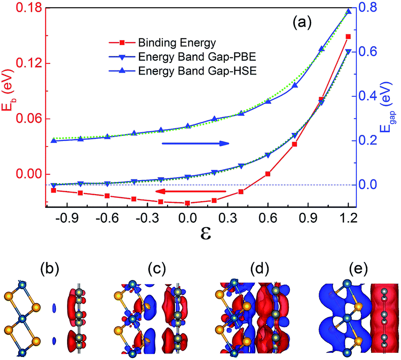 | ||
| Fig. 4 (a) Eb and Egap of the graphene/PtSe2 heterojunction as a function of vertical strains. The olive and green dots represent the fitted exponential curves calculated by PBE and HSE06, respectively. The side views of the differential charge density of the heterojunction under vertical strains of (b) −0.4, (c) 0.4, (d) 0.8 and (e) 1.2 Å. The isovalue chosen to plot the isosurfaces is set at 0.06 e Å−3. | ||
For enlarged ε = −0.2, −0.4, −0.6, −0.8, and −1.0 Å, the corresponding Eb values are −0.030, −0.027, −0.024, −0.020 and −0.018 eV, respectively. Under compressive strain, Eb quickly increases to 0 eV when the distance between the PtSe2 and graphene sheets approaches 2.69 Å (ε = 0.6 Å). When ε > 0.6 Å, Eb becomes positive, implying that the interaction between graphene and PtSe2 becomes repulsive. For ε = 0.8, 1.0, and 1.2 Å, the corresponding Eb values are as large as 0.972, 2.428 and 4.469 eV, respectively, indicating that the repulsive interaction is rapidly enhanced.
The change in the interaction between the PtSe2 and graphene layers caused by the orbital hybridization between them would be reflected by the intensity of the charge transfer between them. To explore the charge transfer process, the differential charge density of the graphene/PtSe2 heterojunction was calculated, as shown in Fig. 4(b)–(e) for the selected strains. For ε = 0 Å (deq = 3.29 Å), there is about a 0.070e amount of charge transferred from PtSe2 to graphene. As the distance between the graphene and PtSe2 sheets decreases, the charge transfer is obviously intensified due to the enhanced hybridization between the pz orbital of graphene and the p orbital of PtSe2, as shown in Fig. S7.† Similar phenomena also appear in other vdW heterojunctions, such as in the C2N/MoS2 vdW heterojunction.52 We also evaluated Δq as a function of strains, as shown in the inset of Fig. 3(c). For ε = 0.4, 0.8, and 1.2 Å, the corresponding Δq was 0.108, 0.196, and 0.387e, respectively. Such enhanced charge transfer under compressive vertical strain is expected to efficiently tune the electronic properties of the graphene/PtSe2 heterojunction.
The calculated electronic band gap at the Γ point (Egap) of the graphene/PtSe2 heterojunction as a function of the vertical strain is shown in Fig. 4(a). As the compressive vertical strain increases, the corresponding Egap monotonously increases, and the physical picture is founded on symmetry-breaking caused by the substrate potential.
For the ε values from −1.0 Å to 1.2 Å, the Egap under PBE as a function of strain is found to follow an exponential relationship: Egap = 0.003 + 0.032 × exp(2.451ε), while under HSE06, a different exponential relationship: Egap = 0.200 + 0.057 × exp(1.936ε) results, and a similar relationship also appears in the graphene/h-BN vdW heterojunction.75 We also calculated the relationship between Egap and vertical strains with DFT + D3, and a similar exponential relationship is also found, as shown in Fig. S8 in the ESI.† The corresponding band structures calculated by HSE06 are shown in Fig. 5. For ε = 0.2, 0.6 and 1.0 Å, the Egap values calculated by HSE06 are 0.297, 0.376, and 0.613 eV, respectively. As the compressive strain increases, the corresponding energies of the VBM at the K point are always increased. When ε = 1.0 Å, the energy of the VBM at the K point (−0.309 eV) is just a little lower than that of the VBM at the Γ point (−0.307 eV). When ε approaches 1.2 Å, the corresponding Egap value is as large as 0.781 eV at the Γ point. Meanwhile, the VBM is shifted from the original Γ point to the K point, so the graphene/PtSe2 heterojunction undergoes a direct-to-indirect band-gap transition, and the indirect gap is 0.467 eV. This is caused by the strong interaction between the sheets and the enhancement of the spin-orbital coupling (SOC) effect, and a similar phenomenon is also observed in the PtSe2 bilayer.76 More details and discussions can be found in Fig. S9 in the ESI.† As the enlarged vertical strain increases, the interlayer interaction becomes weak. So the band gap value of the graphene opened by PtSe2 decreases slowly. As ε is increased from −0.6 to −1.0 Å, the corresponding Egap value monotonously decreases to 0.216 and 0.199 eV, respectively. For larger enlarged vertical strains, graphene should be semimetal for the weak interaction between the sheets. So the vertical strains can effectively tune the electronic properties of the graphene/PtSe2 heterojunction.
 | ||
| Fig. 5 The evolution of the band structures in the graphene/PtSe2 heterojunction calculated by HSE06 as a function of the vertical strains: (a) −0.4, (b) 0.4, (c) 0.8, (d) 1.0, and (e) 1.2 Å. | ||
4 Conclusions
We have comprehensively investigated the structural and electronic properties of the graphene/PtSe2 heterojunction for the first time. Using first-principle calculations, energy-gap engineering has been studied. It is shown that under the inhomogenous electrostatic potential generated by PtSe2, the band gap of graphene is opened by PtSe2, which is as large as 0.264 eV, and sufficient enough to overcome the thermal excitation of electrons at room temperature. At the graphene/PtSe2 interface, a small amount of charge is transferred from PtSe2 to graphene. By applying vertical strain, the interface charge transfer and interlayer interaction in the graphene/PtSe2 heterojunction can be effectively modulated, which means that the band gap of graphene can be enlarged to as large as 0.781 eV. The graphene/PtSe2 heterojunction with a finite band gap and high carrier mobility has high potential to be used as a FET, promoting the application of graphene in nano-electronics.Conflicts of interest
There are no conflicts to declare.Acknowledgements
We thank Prof. Wenhui Duan for useful discussions and suggestion. We are grateful for the financial support from the Natural Science Foundation of China (Grant No. 21503201), the President Foundation of China Academy of Engineering Physics (YZJJLX2016004), and the National Key Research and Development Program of China (under Grants No. 2016YFB0201203). The computational resources from Shanghai Supercomputer Center, National Supercomputing Centers of Guangzhou, and Tsinghua Supercomputer Centers should also be acknowledged.References
- K. S. Novoselov, A. K. Geim, S. Morozov, D. Jiang, Y. Zhang, S. Dubonos, I. Grigorieva and A. Firsov, Science, 2004, 306, 666–669 CrossRef CAS PubMed.
- Y. Zhang, Y. W. Tan, H. L. Stormer and P. Kim, Nature, 2005, 438, 201–204 CrossRef CAS PubMed.
- C. Berger, Z. Song, X. Li, X. Wu, N. Brown, C. Naud, D. Mayou, T. Li, J. Hass, A. N. Marchenkov, E. H. Conrad, P. N. First and W. A. de Heer, Science, 2006, 312, 1191–1196 CrossRef CAS PubMed.
- P. Avouris, Nano Lett., 2010, 10, 4285–4294 CrossRef CAS PubMed.
- M. Xu, T. Liang, M. Shi and H. Z. Chen, Chem. Rev., 2013, 113, 3766–3798 CrossRef CAS PubMed.
- A. H. Castro Neto, N. M. R. Peres and S. K. Novoselov, Rev. Mod. Phys., 2009, 81, 109–162 CrossRef CAS.
- V. P. Gusynin and S. G. Sharapov, Phys. Rev. Lett., 2005, 95, 146801 CrossRef CAS PubMed.
- K. S. Novoselov, Z. Jiang, Y. Zhang, S. V. Morozov, H. L. Stormer, U. Zeitler, J. C. Maan, G. S. Boebinger, P. Kim and A. K. Geim, Science, 2007, 315, 1379 CrossRef CAS PubMed.
- A. J. Du and S. C. Smith, J. Phys. Chem. Lett., 2011, 2, 73–80 CrossRef CAS PubMed.
- G. Brumfiel, Nature, 2009, 458, 390–391 CrossRef CAS PubMed.
- D. V. Kosynkin, A. L. Higginbotham, A. Sinitskii, J. R. Lomeda, A. Dimiev, B. Katherine Price and J. M. Tour, Nature, 2009, 458, 872–876 CrossRef CAS PubMed.
- L. Y. Jiao, L. Zhang, X. R. Wang, G. Diankov and H. J. Dai, Nature, 2009, 458, 877–880 CrossRef CAS PubMed.
- F. Guinea, M. I. Katsnelson and A. K. Geim, Nat. Phys., 2010, 6, 30–33 CrossRef CAS.
- Z. H. Ni, T. Yu, Y. H. Lu, Y. Y. Wang, Y. P. Feng and Z. X. Shen, ACS Nano, 2008, 2, 2301–2305 CrossRef CAS PubMed.
- R. Balog, B. Jorgensen, L. Nilsson, M. Andersen, E. Rienks, M. Bianchi, M. Fanetti, E. Laegsgaard, A. Baraldi and S. Lizzit, et al., Nat. Mater., 2010, 9, 315–319 CrossRef CAS PubMed.
- A. J. Du, Z. H. Zhu and S. C. Smith, J. Am. Chem. Soc., 2010, 132, 2876–2877 CrossRef CAS PubMed.
- C. Si, Z. M. Sun and F. Liu, Nanoscale, 2016, 8, 3207–3217 RSC.
- F. Wang, Y. B. Zhang, C. S. Tian, C. Girit, A. Zettl, M. Crommie and Y. R. Shen, Science, 2008, 320, 206–209 CrossRef CAS PubMed.
- Y. B. Zhang, T. T. Tang, C. Girit, Z. Hao, M. C. Martin, A. Zettl, M. F. Crommie, Y. R. Shen and F. Wang, Nature, 2009, 459, 820–823 CrossRef CAS PubMed.
- H. Miyazaki, K. Tsukagoshi, A. Kanda, M. Otain and S. Okada, Nano Lett., 2010, 10, 3888–3892 CrossRef CAS PubMed.
- Y.-W. Son, M. L. Cohen and S. Louie, Nature, 2006, 444, 347–349 CrossRef CAS PubMed.
- R. Decker, Y. Wang, V. W. Brar, W. Regan, H. Z. Tsai, Q. Wu, W. Gannett, A. Zettl and M. F. Crommie, Nano Lett., 2011, 11, 2291–2295 CrossRef CAS PubMed.
- C. Berger, Z. M. Song, X. B. Li, X. S. Wu, N. Brown, C. Naud, D. Mayou, T. B. Li, J. Hass, A. N. Marchenkov, E. H. Conrad, P. N. First and W. A. de Heer, Science, 2006, 312, 1191–1196 CrossRef CAS PubMed.
- Y. M. Lin, C. Dimitrakopoulos, K. A. Jenkins, D. B. Farmer, H. Y. Chiu and A. Grill, Science, 2010, 327, 662 CrossRef CAS PubMed.
- C. Si, G. Zhou, Y. Li, J. Wu and W. Duan, Appl. Phys. Lett., 2012, 100, 103105 CrossRef.
- L. Liao, Y. C. Lin, M. Q. Bao, R. Cheng, J. W. Bai, Y. Liu, Y. Q. Qu, K. L. Wang, Y. Huang and X. F. Duan, Nature, 2010, 467, 305–308 CrossRef CAS PubMed.
- X. S. Li, W. W. Cai, J. H. An, S. Kim, J. Nah, D. X. Yang, R. Piner, V. Aruna, I. Jung and E. Tutuc, et al., Science, 2009, 324, 1312–1314 CrossRef CAS PubMed.
- Y. Zhang, L. Gomez, F. N. Ishikawa, A. Madaria, R. Koungmin, C. Wang, A. Badmaev and C. W. Zhou, J. Phys. Chem. Lett., 2010, 1, 3101–3107 CrossRef CAS.
- W. J. Zhang, C. P. Huang Chuu, J. K. C. H. Chen, M. L. Tsai, Y. H. Chang, C. Y. Liang, Y. Z. Chen, Y. L. Chueh, J. H. He, M. Y. Chou and L. Y. Li, Sci. Rep., 2014, 4, 3826 CrossRef PubMed.
- P. Khomyakov, A. G. Giovannetti, P. C. Rusu, G. Brocks, J. van den Brink and P. J. Kelly, Phys. Rev. B: Condens. Matter Mater. Phys., 2009, 79, 195425 CrossRef.
- Y. D. Ma, Y. Dai, M. Guo, C. Niu and B. B. Huang, Nanoscale, 2011, 3, 3883–3887 RSC.
- A. J. Du, S. Sanvito, Z. Li, D. W. Wang, Y. Jiao, T. Liao, Q. Sun, Y. H. Ng, Z. H. Zhu, R. Amal and S. C. Smith, J. Am. Chem. Soc., 2012, 134, 4393–4397 CrossRef CAS PubMed.
- W. X. Wang, L. J. Yin, J. B. Qiao, T. C. Cai, S. Y. Li, R. F. Dou, J. C. Nie, X. S. Wu and L. He, Phys. Rev. B: Condens. Matter Mater. Phys., 2015, 92, 165420 CrossRef.
- C. R. Dean, A. F. Young, I. Meric, C. Lee, L. Wang, S. Sorgenfrei, K. Watanabe, T. Taniguchi, P. Kim, K. L. Shepard and J. Hone, Nat. Nanotechnol., 2010, 5, 722–726 CrossRef CAS PubMed.
- N. Kharche and S. K. Nayak, Nano Lett., 2011, 11, 5274–5278 CrossRef CAS PubMed.
- M. Yankowitz, J. M. Xue, D. Cormode, J. D. Sanchez-Yamagishi, K. Watanabe, T. Taniguchi, P. Jarillo-Herrero, P. Jacquod and B. J. LeRoy, Nat. Phys., 2012, 8, 382–386 CrossRef CAS.
- G. Argentero, A. Mittelberger, M. R. A. Monazam, Y. Cao, T. J. Pennycook, C. Mangler, C. Kramberger, J. Kotakoski, A. K. Geim and J. C. Meyer, Nano Lett., 2017, 17, 1409–1416 CrossRef CAS PubMed.
- Y. L. Wang, L. F. Li, W. Yao, S. R. Song, J. T. Sun, J. B. Pan, X. Ren, C. Li, E. J. Okunishi and Y. Q. Wang, et al., Nano Lett., 2015, 15, 4013–4018 CrossRef CAS PubMed.
- C. Y. Yim, K. H. Lee, N. McEvoy, M. O’Brien, S. Riazimehr, N. C. Berner, C. P. Cullen, J. Kotakoski, J. C. Meyer and M. C. Lemme, et al., ACS Nano, 2016, 10, 9550–9558 CrossRef CAS PubMed.
- S. Muhammad, M. Enrique, S. Nirpendra and S. Udo, Adv. Mater. Interfaces, 2017, 1600911 Search PubMed.
- W. X. Zhang, Z. S. Huang, W. L. Zhang and Y. R. Li, Nano Res., 2014, 7, 1731–1737 CrossRef CAS.
- Y. D. Zhao, J. S. Qiao, Z. H. Yu, P. Yu, K. Xu, S. P. Lau, W. Zhou, Z. Liu, X. R. Wang, W. Ji and Y. Chai, Adv. Mater., 2016, 29, 1604230 CrossRef PubMed.
- X. Y. Chia, A. Adriano, P. Lazar, Z. Sofer, J. Luxa and M. Pumera, Adv. Funct. Mater., 2016, 26, 4306–4318 CrossRef CAS.
- W. Yao, E. Y. Wang, H. Q. Huang, K. Deng, M. Z. Yan, K. N. Zhang, K. Miyamoto, T. Okuda, L. Y. Li and Y. L. Wang, et al., Nat. Commun., 2017, 8, 14216 CrossRef CAS PubMed.
- H. Q. Huang, S. Y. Zhou and W. H. Duan, Phys. Rev. B: Condens. Matter Mater. Phys., 2016, 94, 121117(R) CrossRef.
- T. Bučko, J. Hafner, S. Lebegue and J. G. Angyan, J. Phys. Chem. A, 2010, 114, 11814–11824 CrossRef PubMed.
- S. Grimme, J. Antony, S. Ehrlich and S. Krieg, J. Chem. Phys., 2010, 132, 154104 CrossRef PubMed.
- G. Kresse and J. Furthmüller, Comput. Mater. Sci., 1996, 6, 15–50 CrossRef CAS.
- G. Kresse, Phys. Rev. B: Condens. Matter Mater. Phys., 1996, 54, 11169–11186 CrossRef CAS.
- J. P. Perdew, K. Burke and M. Ernzerhof, Phys. Rev. Lett., 1996, 77, 3865–3868 CrossRef CAS PubMed.
- R. Zhang, B. Li and J. Yang, J. Phys. Chem. C, 2015, 119, 2871–2878 CAS.
- Z. Y. Guan, C. S. Lian, S. L. Hu, S. Ni, J. Li and W. H. Duan, J. Phys. Chem. C, 2017, 12, 3654–3660 Search PubMed.
- Y. Baskin and L. Meyer, Phys. Rev., 1955, 100, 544 CrossRef CAS.
- A. K. Geim and K. S. Novoselov, Nat. Mater., 2007, 6, 183–191 CrossRef CAS PubMed.
- D. W. Boukhvalov and M. I. Katsnelson, Phys. Rev. B: Condens. Matter Mater. Phys., 2008, 78, 085413 CrossRef.
- T. Olsen and K. S. Thygesen, Phys. Rev. B: Condens. Matter Mater. Phys., 2013, 88, 115131 CrossRef.
- A. Ambrosetti, N. Ferri, R. A. DiStasio Jr and A. Tkatchenko, Science, 2016, 351, 1171–1176 CrossRef CAS PubMed.
- A. Ambrosetti, P. L. Silvestrelli and A. Tkatchenko, Phys. Rev. B: Condens. Matter Mater. Phys., 2017, 95, 235417 CrossRef.
- H. Eshuis, J. E. Bates and F. Furche, Theor. Chem. Acc., 2012, 131, 1084 CrossRef.
- Y. M. He, Y. Yang, Z. H. Zhang, Y. J. Gong, W. Zhou, Z. L. Hu, G. L. Ye, X. Zhang, E. Bianco and S. D. Lei, et al., Nano Lett., 2016, 16, 3314–3320 CrossRef CAS PubMed.
- S. Daniele, N. R. Papior, O. Hansen and M. Brandbyge, Nano Lett., 2017, 17, 2660–2666 CrossRef PubMed.
- J. Heyd, G. E. Scuseria and M. Ernzerhof, J. Chem. Phys., 2003, 118, 8207 CrossRef CAS.
- J. Paier, M. Marsman, K. Hummer, G. Kresse, I. C. Gerber and J. G. Angyan, J. Chem. Phys., 2006, 124, 154709–154722 CrossRef CAS PubMed.
- P. Lazie, Comput. Phys. Commun., 2015, 197, 324 CrossRef.
- H. L. L. Zhuang and R. G. Hennig, J. Phys. Chem. C, 2013, 117, 20440–20445 CAS.
- N. T. Cuong, M. Otani and S. Okada, Phys. Rev. Lett., 2011, 106, 106801 CrossRef PubMed.
- X. H. Zheng, X. L. Wang, L. F. Huang, H. Hao, J. Lan and Z. Zeng, Phys. Rev. B: Condens. Matter Mater. Phys., 2013, 87, 165415 CrossRef.
- E. J. Kan, H. Ren, F. Wu, Z. Y. Li, R. F. Lu, C. Y. Xiao, K. M. Deng and J. L. Yang, J. Phys. Chem. C, 2012, 116, 3142–3146 CAS.
- J. Jeil, M. D. Ashley, H. MacDonald Allan and A. Shaffique, Nat. Commun., 2015, 6, 6308 CrossRef PubMed.
- E. Y. Wang, X. B. Lu, S. J. Ding, W. Yao, M. Z. Yan, G. L. Wan, K. Deng, S. P. Wang, G. R. Chen, L. G. Ma and J. Jung, et al., Nat. Phys., 2016, 12, 1111–1115 CrossRef CAS.
- K. S. Novoselov, D. Jiang, F. Schedin, T. J. Booth, W. Khotkevich, S. V. Morozov and A. K. Geim, Proc. Natl. Acad. Sci. U. S. A., 2005, 102, 10451–10453 CrossRef CAS PubMed.
- Y. Matthew, K. Watanabe, T. Taniguchi, P. San-Jose and J. L. Brian, Nat. Commun., 2016, 7, 13168–13175 CrossRef PubMed.
- X. G. Liu and Z. Y. Li, J. Phys. Chem. Lett., 2015, 6, 3669–3675 Search PubMed.
- F. W. Chen, H. Ilatikhameneh, G. Klimeck, R. Rahman, T. Chu and Z. H. Chen, Simulation of Semiconductor Processes and Devices (SISPAD), 2015 International Conference on IEEE, 2015, pp. 177–181 Search PubMed.
- G. Giovannetti, P. A. Khomyakov, G. Brocks, P. J. Kelly and J. van den Brink, Phys. Rev. B: Condens. Matter Mater. Phys., 2007, 76, 073103 CrossRef.
- S. D. Guo, J. Mater. Chem. C, 2016, 4, 9366–9374 RSC.
Footnote |
| † Electronic supplementary information (ESI) available. See DOI: 10.1039/c7ra06865d |
| This journal is © The Royal Society of Chemistry 2017 |