
 Open Access Article
 This Open Access Article is licensed under a
 Creative Commons Attribution 3.0 Unported Licence
Encapsulation of transition metal dichalcogenides crystals with room temperature plasma deposited carbonaceous films†
Rakesh D. Mahyavanshi *a,
Golap Kalita*a,
Rupesh Singhc,
Masaharu Kondob,
Takehisa Dewab,
Toshio Kawaharac,
Masayoshi Umenoc and
Masaki Tanemuraa
*a,
Golap Kalita*a,
Rupesh Singhc,
Masaharu Kondob,
Takehisa Dewab,
Toshio Kawaharac,
Masayoshi Umenoc and
Masaki Tanemuraa
aDepartment of Physical Science and Engineering, Nagoya Institute of Technology, Gokiso-cho, Showa-ku, Nagoya 466-8555, Japan. E-mail: rmahyavanshi@gmail.com; kalita.golap@nitech.ac.jp; Fax: +81-527355216; Tel: +81-527355216
bDepartment of Life Science and Applied Chemistry, Nagoya Institute of Technology, Gokiso-cho, Showa-ku, Nagoya 466-8555, Japan
cDepartment of Electronics and Information Engineering, Chubu University, 1200 Matsumoto-cho, Kasugai, 487-8501, Japan
First published on 22nd August 2017
Abstract
Encapsulation and its effect on two-dimensional (2D) dichalcogenides layered materials are of significant importance for electronic device fabrication. Here, we developed a dry and rapid encapsulation method for the 2D dichalcogenides by coating a carbonaceous film at room temperature using a plasma technique. Thin encapsulation film is coated on dichalcogenide crystals by microwave assisted surface wave plasma (MW-SWP) chemical vapor deposition (CVD) within a very short duration. Photoluminescence (PL) analysis shows the influence on excitation as well as the emission light with the coating of a carbonaceous film. The encapsulated dichalcogenide samples remain intact after heating at 200 °C as observed by PL and microscopic analysis. We also demonstrate obtaining stable photoconductivity for the dichalcogenide layers with encapsulation of a carbonaceous film. The rapid and dry coating technique at room temperature can be extended to various other 2D materials as the MW-SWP process allows damage-free encapsulation.
1. Introduction
In recent years, transition metal dichalcogenides (TMDCs) and other two-dimensional (2D) layered materials have attracted significant interest for nanoelectronic and optoelectronic device applications.1–5 The TMDCs are a large family of semiconductors (e.g. MoS2, WS2 etc.), metals (e.g. TiS2, VSe2), superconductors (e.g. TaS2, NbSe2), semimetals (e.g. WTe2 and TiSe2) and insulators (e.g. HfS2).6–16 The thickness dependent electronic and optoelectronic properties of group VI dichalcogenides (MX2, M = Mo, W; X = S, Se, etc.) semiconductors are quite promising for novel optoelectronic devices.17,18 Transition from indirect band gap to direct band gap for the semiconducting trigonal prismatic MX2 has been revealed as the thickness reduces to monolayer.19–22 The MX2 semiconductor with excellent optical absorption in visible range and large exciton binding energy has attracted wide attention for high-performance photodetectors, efficient solar cells, and multifunctional nanoelectronics.23–26 TMDCs layered materials have been derived by exfoliation process, hydrothermal synthesis and chemical vapor deposition (CVD) techniques.27–30 The CVD technique has a significant advantage for the synthesis of large-area polycrystalline films, single crystal domains, vertical or lateral heterostructures of two different dichalcogenides.29–32Recent studies show structural transformation and degradation of MX2 layered materials with oxygen exposure, UV irradiation, ozone exposure and heating under ambient conditions.33–36 Significant structural degradation of MX2 layers has been also observed with long-term exposure to ambient conditions.36 The other 2D layered semiconductors, such as black phosphorus are more unstable and degradable under ambient conditions.37 In this context, encapsulation and device engineering are the key aspects that need to be addressed in the coming years for practical application of these layered semiconductors. Gao et al., has demonstrated coating of poly(methyl methacrylate) (PMMA) and Parylene C on MoS2 and WS2 layers to protect from ageing.36 Ahn et al. has demonstrated the transferring process of PMMA/h-BN layer on WSe2 layer as degradation protective layer.38 Recently, Woodhead et al. have developed an optical solution to encapsulate monolayer MX2 from physical damage and degradation.39 It has been also reported that depending on the layered materials a compressive or other lattice strain can be observed with the encapsulation layer.39,40 In contrast to the previous reports, we developed a rapid and dry approach to fully encapsulate MX2 layered materials preventing degradation in ambient conditions. As follows, we demonstrate the encapsulation and PL emission properties with the plasma CVD deposited carbonaceous film on MX2 layers.
2. Experimental section
2.1 Synthesis of MoS2 and WS2 crystals
MoS2 and WS2 crystals were grown on SiO2/Si substrate by thermal chemical vapor deposition (CVD) method by controlling the growth parameters. The synthesis was performed in a quartz tube CVD system with a mixture of argon (Ar) and H2 gas flow at atmospheric pressure. Prior to the thermal CVD growth, the substrate was cleaned using acetone and following isopropyl alcohol (IPA) for 15 min each by sonication. Sulfur powder (1 g) in a ceramic boat was inserted into the quartz tube of length 90 cm and diameter of 4.5 cm. It was placed in a low-temperature furnace (LTF) heated to 180 °C. The substrate and MoO3 and WO3 powder (10 mg) were kept on a ceramic boat for the growth of MoS2 and WS2 crystals, respectively in two separate experiments. MoS2 and WS2 crystals were synthesized at 750 and 850 °C, respectively in the high-temperature furnace (HTF). Both the experiments were carried out using 100 standard cubic centimeters per minute (sccm) of argon and H2 gas mixture (97![[thin space (1/6-em)]](https://www.rsc.org/images/entities/char_2009.gif) :3).
:3).
2.2 Deposition of a carbonaceous film by plasma CVD
Carbonaceous film was deposited by microwave assisted surface wave plasma (MW-SWP) chemical vapor deposition (CVD) technique on the MoS2 and WS2 crystals synthesized on SiO2/Si substrates. A metal grid was placed above the MoS2 and WS2 crystal samples (Fig. S1†) to avoid plasma induced deformation of the TMDCs layers. The MW-SWP CVD chamber was evacuated to 5 × 10⁻⁴ Pa prior to the deposition. The thin film deposition was performed at 10–20 Pa gas composition pressure with a flow rate of 100–200 sccm of Ar and 10–50 sccm of CH4. The microwave power was fixed as 800 W with negligible amount of fluctuation. Deposition of the thin films was carried out for a duration of 60–240 s at room temperature (∼24 °C).2.3 Characterization of prepared samples
Prepared samples were characterized by optical microscopy, Raman spectroscopy, field-emission scanning electron microscopy (FE-SEM), photoluminescence (PL) spectroscopy and X-ray photoelectron spectroscopy (XPS). Optical microscopy analysis was performed using the digital optical microscope VHX-500 in reflectance mode with a Moticam 2000 2.0 M pixel camera. Raman analysis was carried out using the NRS 3300 laser Raman spectrometer with a laser excitation wavelength of 532.08 nm. FE-SEM study was performed with JEOL JSM-7800F with an accelerating voltage of 5 kV. Infrared (IR) spectroscopy analysis was carried out with grazing incident using JASCO IRT-5000 FT-IR microscope. Absorbance and transmittance of the carbonaceous film was measured by JASCO V-670K spectrophotometer. XPS analysis was performed by VersaProbe using monochromated Al Kα excitation source (1486.6 eV). PL analysis was carried with a confocal laser scanning microscope (NX-3DFLIM-N03, Tokyo Instruments, Japan) equipped with a Nd:YVO4 diode laser. For the device fabrication, Au electrodes were deposited by the thermal evaporation technique using ULVAC VPC-260F. The current–voltage (I–V) characteristics were measured using a two probe system and a Keithley 2401 SourceMeter.3. Results and discussion
Fig. 1a shows optical microscope image of MoS2 crystal synthesized on the SiO2/Si substrate by thermal CVD technique. Triangular shaped MoS2 crystals with curved edges and size of around 20 μm were obtained in the particular growth condition. Fig. 1b shows an AFM image of the as-synthesized MoS2 crystal. The line profile shows a thickness of nearly ∼0.9 nm for the individual MoS2 crystals. The synthesized samples were transferred to MW-SWP CVD chambers for coating without any other treatment. Microwave excited plasma sources have been used for effective deposition of an insulating encapsulation layer for the conventional semiconductors.41,42 We explore the possibility of 2D layered materials encapsulation at room temperature by SW-MWP technique. The MW-SWP can produce an over-dense plasma even at a low gas pressure, with a density higher than the cut-off density (7.4 × 10¹⁶ m−3 for 2.45 GHz). The deposition process was rapid and substrates were place at a longer distance from plasma shower which allowed to maintain the substrate temperature at ∼24 °C. Fig. 1c shows an optical microscope image of the coated MoS2 crystals. The triangular MoS2 crystal remain intact without any visible structural damage. Fig. 1d shows a higher resolution optical microscopy image of the MoS2 triangular crystals, where the morphology is unaffected by deposition of the encapsulation film. Unlike other plasma technique, the MW-SWP is a promising tool for large-area carbonaceous film deposition and useful to avoid plasma induced damages of the substrate surface.43 The details of the deposition process and photograph of the deposited film are included in ESI (Fig. S1 and S2†).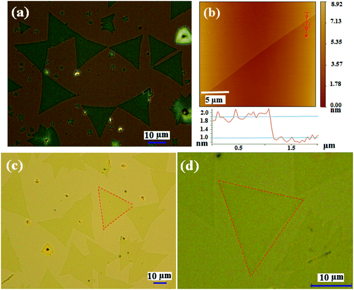 | ||
| Fig. 1 (a) Optical microscope images of as-synthesized MoS2 crystals on the SiO2/Si substrate. (b) AFM image of MoS2 crystal and line profile presenting the thickness. Optical microscope images of carbonaceous film coated (c) MoS2 crystals and (d) higher resolution view of a triangular MoS2 crystal. | ||
Fig. 2a shows an IR absorption spectra of the carbonaceous film coated on the MoS2/SiO2/Si sample (∼15 nm). Few weak peaks are observed in the frequency range from 1300 to 1600 cm−1, where the peak centered at ∼1530 cm−1 can be assigned to C![[double bond, length as m-dash]](https://www.rsc.org/images/entities/char_e001.gif) C stretching vibrations. At a higher frequency range, three sharper peaks at 2870, 2925 and 2961 cm−1 were observed corresponding to the C–H vibrations. These absorption peaks can be assigned to sp3 CHx symmetric and asymmetric bands. Fig. 2b shows a typical Raman spectra of the carbonaceous coating. There was no significant Raman features for the plasma deposited carbonaceous film, other than a broad hump and reduction in intensity of Si Raman peak. A carbon film coated around ∼150 °C with similar plasma parameters shows broad D and G peaks, clearly indicating the difference in carbon structures for room temperature deposited film (Fig. S3†). The presence of sp3 CHx bonds and no clear Raman peaks (D and G bands) signifies formation of insulating carbonaceous film with polymeric nature.43,44 The room temperature deposited carbon film is significantly different than that of normal crystalline and amorphous carbon forms. Fig. 2c shows transmittance and absorbance of the carbonaceous film deposited on glass substrate. The coated film shows excellent transparency in the wavelength range of 0.3–2 μm. More than 95% transparency is obtained in the visible light region, which can be tuned with appropriate thickness of the deposited film. The coated film on SiO2/Si substrate was characterized by Raman spectroscopy with and without the TMDCs crystals. Fig. 2d and e shows Raman spectra of the MoS2 crystals with and without encapsulated film. The Raman vibration modes E12g and A1g for MoS2 are observed at 383.2 and 403.3 cm−1, (frequency difference of ∼20 cm−1) corresponding to in-plane vibration of molybdenum and sulfur and out-of-plane vibration of sulfur atoms, respectively. We observed a reduction in Raman peak intensity for the encapsulated sample, while no significant shift in peak position. Influence of the coated layer was further analyzed by PL study to investigate the possible effect on PL excitation and light emission.
C stretching vibrations. At a higher frequency range, three sharper peaks at 2870, 2925 and 2961 cm−1 were observed corresponding to the C–H vibrations. These absorption peaks can be assigned to sp3 CHx symmetric and asymmetric bands. Fig. 2b shows a typical Raman spectra of the carbonaceous coating. There was no significant Raman features for the plasma deposited carbonaceous film, other than a broad hump and reduction in intensity of Si Raman peak. A carbon film coated around ∼150 °C with similar plasma parameters shows broad D and G peaks, clearly indicating the difference in carbon structures for room temperature deposited film (Fig. S3†). The presence of sp3 CHx bonds and no clear Raman peaks (D and G bands) signifies formation of insulating carbonaceous film with polymeric nature.43,44 The room temperature deposited carbon film is significantly different than that of normal crystalline and amorphous carbon forms. Fig. 2c shows transmittance and absorbance of the carbonaceous film deposited on glass substrate. The coated film shows excellent transparency in the wavelength range of 0.3–2 μm. More than 95% transparency is obtained in the visible light region, which can be tuned with appropriate thickness of the deposited film. The coated film on SiO2/Si substrate was characterized by Raman spectroscopy with and without the TMDCs crystals. Fig. 2d and e shows Raman spectra of the MoS2 crystals with and without encapsulated film. The Raman vibration modes E12g and A1g for MoS2 are observed at 383.2 and 403.3 cm−1, (frequency difference of ∼20 cm−1) corresponding to in-plane vibration of molybdenum and sulfur and out-of-plane vibration of sulfur atoms, respectively. We observed a reduction in Raman peak intensity for the encapsulated sample, while no significant shift in peak position. Influence of the coated layer was further analyzed by PL study to investigate the possible effect on PL excitation and light emission.
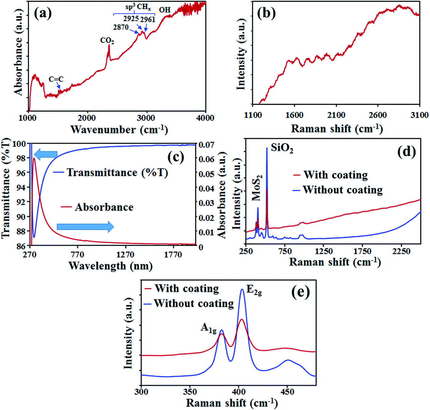 | ||
| Fig. 2 (a) IR (b) Raman (c) transmittance and absorbance spectra of the carbonaceous film on SiO2/Si and glass substrates, deposited along with the coating of TMDCs crystals samples. Raman spectra of the (d) MoS2 crystal on SiO2/Si substrate (e) A1g and E2g peaks with and without encapsulation film. | ||
Fig. 3a shows FE-SEM image of the as-synthesized MoS2 crystals on SiO2/Si substrate by the CVD technique. The triangular shaped MoS2 crystals can be confirmed by the FE-SEM analysis. Fig. 3b shows the FE-SEM image of the plasma deposited carbonaceous film on MoS2 crystals. The surface morphology of the encapsulated MoS2 sample was observed by FE-SEM analysis using the upper electron detector (UED) and 2 kV accelerating voltage. The triangular MoS2 crystals can be confirmed below the encapsulation layer, although the non-conducting encapsulation film significantly affects the micrograph. Previously, plasma functionalization of TMDCs layer has been also demonstrated for modification of electronic properties. PL properties of the encapsulated MoS2 layer were investigated considering the surface functionalization by the plasma process and possible effect on PL emission.45 Fig. 3c shows the PL spectra of coated and non-coated MoS2 crystal. Quenching and red shift of the PL peak for the encapsulated MoS2 sample was observed (Fig. 3c). The PL quenching and shift confirm influence of PL excitation and emission of light for the MoS2 crystal with the encapsulation. Woodhead et al. have also reported significant suppression of the PL peak of MoS2 monolayer by solution coated epoxy due to the compressive strain.39 Compressive strain can modulate the direct to indirect band gap of MoS2 crystals, which reduces the emission intensity. The required values of strain to induce a shift from direct to indirect bandgaps for MoS2 and WS2 are 0.5% and 1% respectively.22 However, the reduction and red shift of the PL peak with the carbonaceous encapsulated layer cannot solely confirm as compressive strain, which was further investigated for the triangular WS2 crystals.
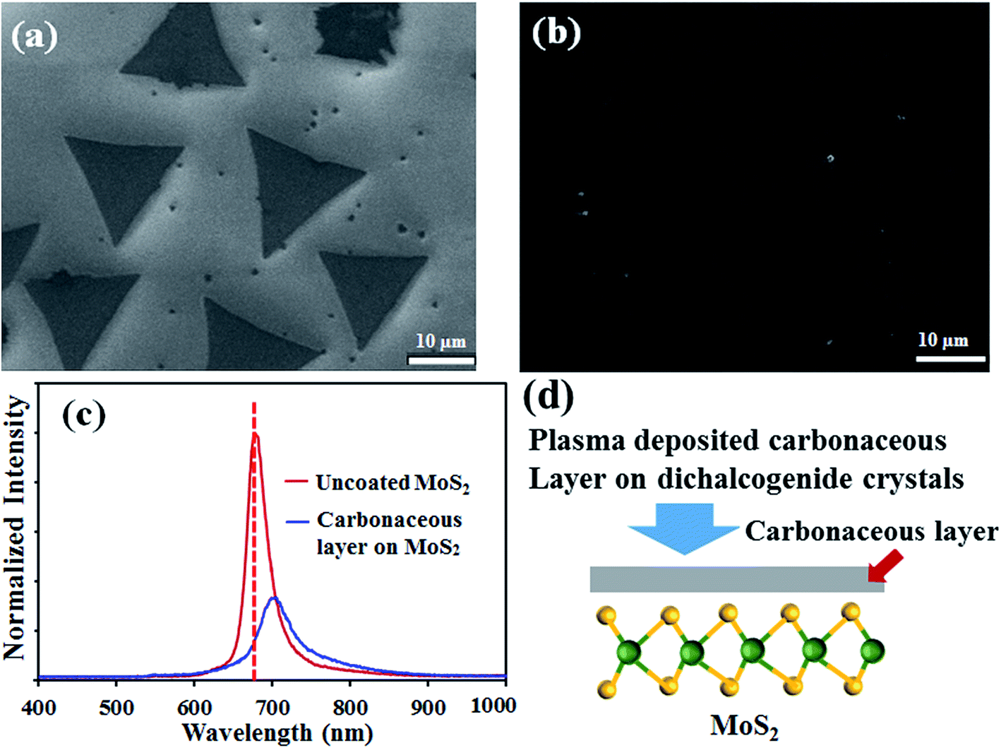 | ||
| Fig. 3 FE-SEM image of (a) as-synthesized and (b) carbonaceous film coated MoS2 crystals. (c) Photoluminescence (PL) spectra of the uncoated and coated MoS2 crystal. (d) Schematic of plasma deposited carbonaceous film encapsulation on MoS2 crystal. | ||
Fig. 4a shows optical microscope image of CVD synthesized triangular WS2 crystals on SiO2/Si substrate. Fig. 4b shows optical microscope image of WS2 crystals on the SiO2/Si substrate after coating a thin carbonaceous film (∼15 nm). Similarly, Fig. 4c shows an optical microscope image of WS2 sample with a thicker coated layer (∼30 nm). The difference in coating thickness can be also identified with variation in contrast of the optical images. The WS2 crystals remain unaffected after the room temperature deposited encapsulation layer as observed from the optical microscopy images. Further, Raman and X-ray photoelectron spectroscopy (XPS) analysis were carried out to investigate the structural properties. XPS analysis of the as growth dichalcogenide layers and encapsulated samples are included in ESI (Fig. S4 and S5†). Fig. 4d shows the Raman spectra of the WS2 crystals before and after coating the encapsulation layer. The as-synthesized WS2 crystals on SiO2/Si substrate shows characteristic Raman shift at ∼356 and ∼423 cm−1 corresponding to E2g mode for in-plane vibration of tungsten and sulfur atoms and A1g mode for out-of-plane vibration of sulfur atoms, respectively. Although, the Raman shift does not show any considerable change from the original sample, the intensity of Raman peak show reduction with increasing thickness of encapsulation layer. The structure and the chemical nature of the WS2 crystals is virtually unaffected by carbonaceous coating as the Raman vibration modes are at the same frequency for as synthesized as well as coated samples. Raman analysis also does not show substantial evidence of strain, while significant reduction and shift of PL peak were evident.36,39,46,47 Fangfei Li et al. has reported only small shift in Raman peaks with applying a significantly high pressure (0.84 GPa) to induce a compressive strain.46
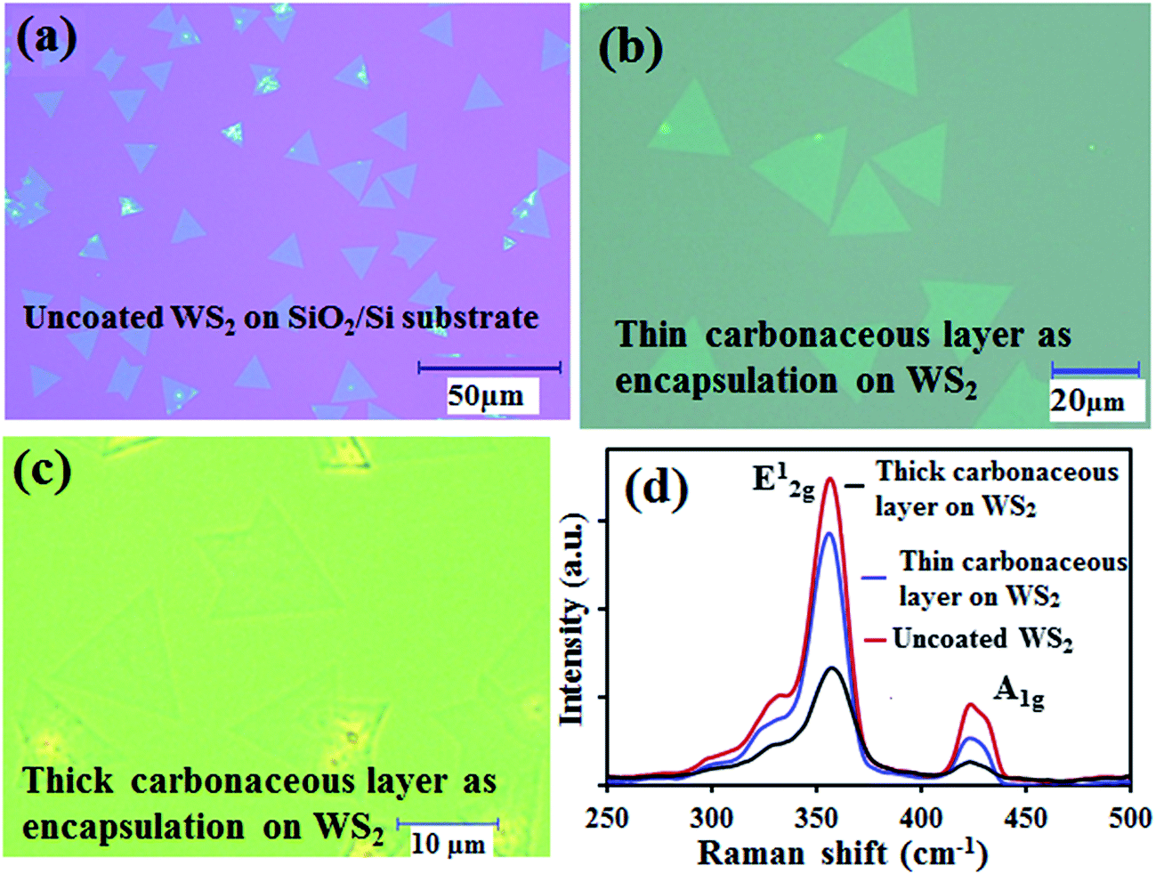 | ||
| Fig. 4 Optical microscope image of (a) CVD synthesized triangular WS2 crystals on SiO2/Si substrate, (b) and (c) MW-SWP deposited carbonaceous film on the CVD synthesized WS2 crystals with different thickness. (d) Raman spectra of the WS2 crystal before and after encapsulation. | ||
The encapsulation behavior of WS2 crystals with the plasma deposited carbonaceous film was investigated by accelerated heating test in atmospheric condition. Fig. 5a shows FE-SEM image of a pristine triangular WS2 crystals after heating in atmosphere at 200 °C for 1 hour. White traces and their branched structures appear thought-out the crystals, signifying the heat-induced degradation of the MX2 layer under atmospheric conditions. Fig. 5b shows FE-SEM image of the encapsulated WS2 crystals after the same accelerated heating test. The triangular WS2 crystals remain intact, however, it is difficult to identify any kind of traces as observed for the uncoated sample due to the presence of the encapsulation layer. PL analysis was carried out to investigate the encapsulation effect of the WS2 crystals before and after the heating of the samples. Fig. 5c shows PL spectra for the uncoated and encapsulated WS2 samples. The intensities were normalized for maximum value to obtain a clear idea of the relative changes in PL. A sharp PL peak at 655 nm (1.89 eV) was obtained for the pristine WS2 crystals. Significant difference in PL peak was observed with coating a carbonaceous layer on the WS2 crystals. Coating a thin encapsulation layer (∼15 nm) on the WS2 crystals, decrease in PL intensity and red shift (shifted to 662 nm corresponding to 1.87 eV) was observed (Fig. 5c). By increasing the thickness of the encapsulation layer (∼30 nm), we observed a much reduced PL peak with the similar red shift. It confirms the influence of the carbonaceous film thickness on the PL excitation as well as the emitted light. Then, PL analysis was performed for the coated and uncoated WS2 samples after heating at 200 °C in atmospheric condition. Fig. 5d shows the normalized PL spectra for the heating tested samples. After the heating process, both the encapsulated WS2 samples show similar intensity PL peaks with a peak position at 650 nm (1.90 eV). The PL peak of the uncoated WS2 crystals was reduced due to the degradation under atmospheric heating as observed from the SEM analysis. Interestingly, the PL peak position of the coated sample slightly blue shifted (∼5 nm) and significantly differed prior to the heating (∼12 nm). The effect is complicated to understand, as different process can occurs, such as reduction in internal absorption of emitted light and change in induced strain.48 Then, the coated samples were further tested by heating at a higher temperature (250 °C) in atmospheric condition. Fig. 5e shows the optical image of the carbonaceous coated WS2 sample after the heating experiment. We observed crack formation in some of the WS2 crystals after the heating process. Fig. 6d shows a higher magnified view of the coated WS2 crystals with clearly visible cracks. The cracks appeared in the WS2 crystals, which propagate in hexagonal patterns, with nearly 120° angles. This signifies localized heat induced defect enhancement in the individual encapsulated WS2 crystals.36 Significantly, we observed the appearance of the cracks only in few WS2 crystals, where all other crystals remain unaffected. The reason behind this anomaly can be attributed to the difference in defect level of individual crystals and variation in induced strain with thermal expansion differences. It can be expected that better thermal conductivity of the TMDCs crystals will lead to relatively higher local temperature of WS2 than the other areas of carbonaceous encapsulated sample. Previously, Yan et al. has reported the local heat induced thermal expansion properties of the TMDCs layer.40
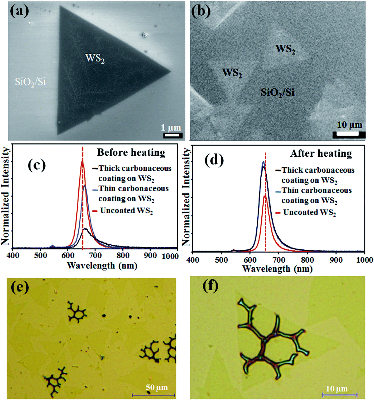 | ||
| Fig. 5 FE-SEM images of triangular WS2 crystals (a) without and (b) with coating a carbonaceous film after heating in atmosphere at 200 °C for 1 hour. PL spectra for (c) before and (d) after heating of the WS2 crystals with different thickness of encapsulation layers in comparison with uncoated sample. Optical microscope images of encapsulated (e) WS2 sample and (f) cracks formation in a WS2 crystals after heating in atmosphere at 250 °C. | ||
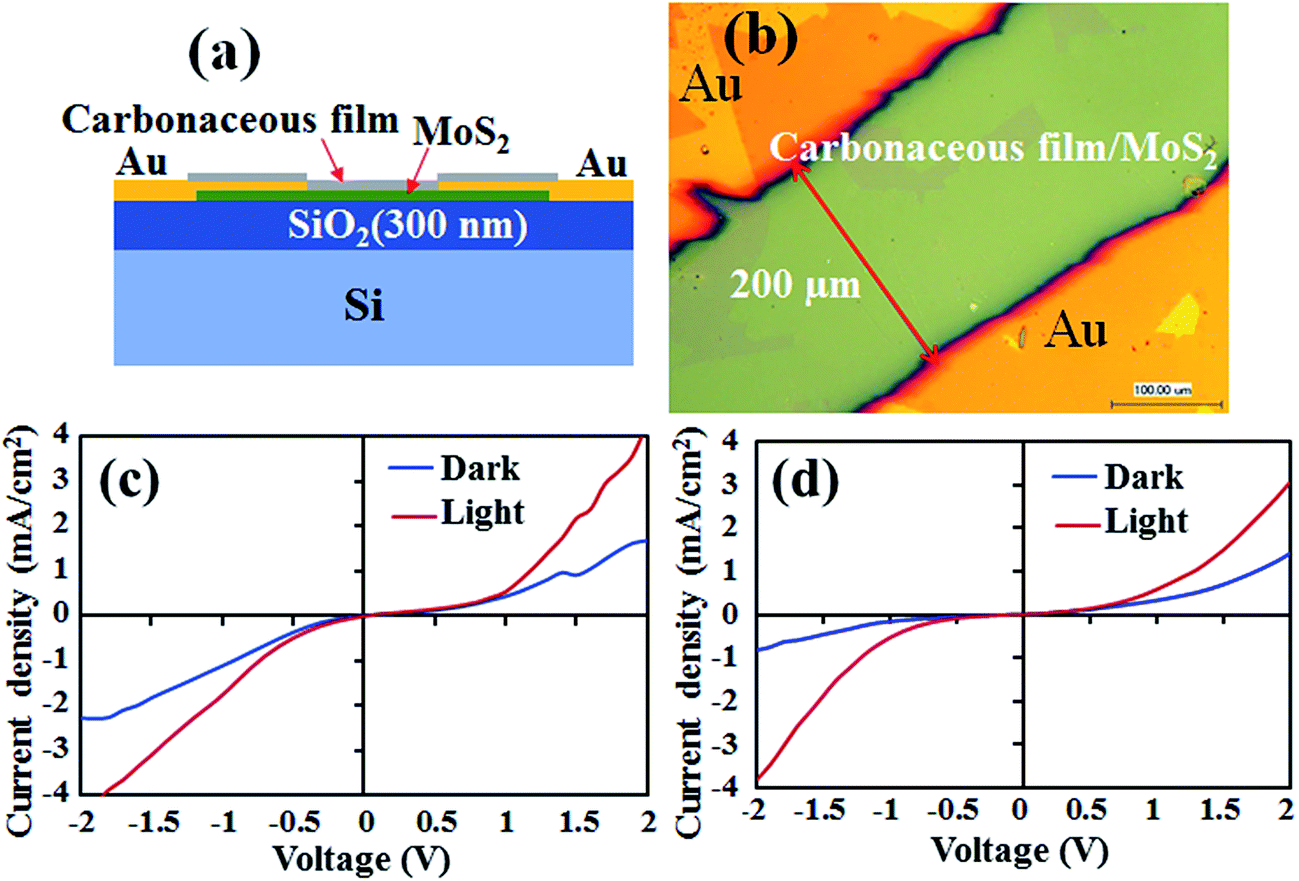 | ||
| Fig. 6 (a) Schematic diagram and (b) optical microscope image of Au/MoS2/Au device with encapsulating carbonaceous layer. Current–voltage (I–V) characteristics of (c) as-fabricated and (d) after annealing at 200 °C for 1 h Au/MoS2/Au device under dark and light illumination. | ||
The effect of encapsulation layer on electrical and optical properties of MoS2 was studied by Schottky junction fabrication. Fig. 6a shows the schematic diagram of the Au/MoS2/Au device with the carbonaceous layer. The distance between two Au electrodes was approximately 200 μm covering MoS2 layer in between as shown in the optical microscope image (Fig. 6b). I–V characteristics of the device was measured with (white light, ∼100 mW cm−2) and without light illumination conditions. Fig. 6c shows I–V characteristic under dark and light conditions of the as-fabricated device with plasma deposited encapsulated layer. Nonlinear Schottky junction behavior was obtained for the semiconducting MoS2 layer and Au metal electrode, where the encapsulated layer did not show much influence on junction behavior. With illumination of light, we observed significant photo-response for Schottky junction with photo-exciton in the MoS2 layer. Then, the device was annealed at 200 °C under atmospheric condition for 1 h as discussed above. Fig. 6d shows I–V characteristic of the same device after annealing. The Schottky junction behavior and photo-responsivity was unchanged and no hysteresis was observed with the annealing in presence of the encapsulating layer. Thus, the effectiveness of carbonaceous encapsulating layer on electrical and photo-responsive properties of MoS2 layer was confirmed.
4. Conclusion
In conclusion, we have demonstrated deposition of a carbonaceous film at room temperature on MoS2 and WS2 crystals by the SW-MWP CVD technique as an encapsulation layer. The encapsulation process is dry, rapid and nondestructive, which can be carried out at room temperature for large area substrate. PL analysis showed the influence on excitation as well as the emission light with the coating of a carbonaceous film. The encapsulated samples remained intact as observed by the optical microscopy, SEM and PL analysis in an accelerated degradation test by heating in ambient condition (humidity ∼65%). We also observed change in PL emission for the encapsulated WS2 layer after heating process, attributing to reduction in internal absorption of emitted light and change in induced strain. We have also demonstrated obtaining stable photoconductivity for the TMDCs dichalcogenide layers with encapsulation of a carbonaceous film. The rapid and dry coating technique at room temperature can be extended to various other 2D materials as MW-SWP process allows damage free encapsulation.Conflicts of interest
There are no conflicts to declare.References
- K. F. Mak, C. Lee, J. Hone, J. Shan and T. F. Heinz, Phys. Rev. Lett., 2010, 105, 136805 CrossRef PubMed.
- Q. H. Wang, K. Kalantar-Zadeh, A. Kis, J. N. Colema and M. S. Strano, Nat. Nanotechnol., 2012, 7, 699–712 CrossRef CAS PubMed.
- K. S. Novoselov, A. K. Geim, S. V. Morozov, D. Jiang, Y. Zhang, S. V. Dubonos, I. V. Grigorieva and A. A. Firsov, Science, 2004, 306, 666–669 CrossRef CAS PubMed.
- P. Vogt, P. De Padova, C. Quaresima, J. Avila, E. Frantzeskakis, M. C. Asensio, A. Resta and B. G. Le Lay, Phys. Rev. Lett., 2012, 108, 155501 CrossRef PubMed.
- L. Li, Y. Yu, G. Jun Ye, Q. Ge, X. Ou, H. Wu, D. Feng, X. H. Chen and Y. Zhang, Nat. Nanotechnol., 2014, 9, 372–377 CrossRef CAS PubMed.
- Z. Y. Zeng, C. L. Tan, X. Huang, S. Y. Bao and H. Zhang, Energy Environ. Sci., 2014, 7, 797–803 CAS.
- F. Y. Li, K. X. Tu and Z. F. Chen, J. Phys. Chem. C, 2014, 118, 21264–21274 CAS.
- L. Ma, C. Ye, Y. Yu, X. F. Lu, X. Niu, S. Kim, D. Feng, D. Tomanek, Y. W. Son, X. H. Chen and Y. Zhang, Nat. Commun., 2016, 7, 10956 CrossRef CAS PubMed.
- X. Xi, L. Zhao, Z. Wang, H. Berger, L. Forro, J. Shan and K. F. Mak, Nat. Nanotechnol., 2015, 10, 765–769 CrossRef CAS PubMed.
- M. M. Ugeda, A. J. Bradley, Y. Zhang, S. Onishi, Y. Chen, W. Ruan, C. Ojeda-Aristizabal, H. Ryu, M. T. Edmonds, H. Z. Tsai, A. Riss, S. K. Mo, D. H. Lee, A. Zettl, Z. Hussain, Z. X. Shen and M. F. Crommie, Nat. Phys., 2016, 12, 92–97 CrossRef CAS.
- T. R. Chang, S. Y. Xu, G. Chang, C. C. Lee, S. M. Huang, B. Wang, G. Bian, H. Zheng, D. S. Sanchez and I. Belopolski, et al., Nat. Commun., 2016, 7, 10639 CrossRef CAS PubMed.
- K. Sugawara, Y. Nakata, R. Shimizu, P. Han, T. Hitosugi, T. Sato and T. Takahashi, ACS Nano, 2016, 10, 1341–1345 CrossRef CAS PubMed.
- Y. I. Joe, X. M. Chen, P. Ghaemi, K. D. Finkelstein, G. A. de la Pena, Y. Gan, J. C. T. Lee, S. Yuan, J. Geck and G. J. MacDougall, et al., Nat. Phys., 2014, 10, 421–425 CrossRef CAS.
- B. Radisavljevic, A. Radenovic, J. Brivio, V. Giacometti and A. Kis, Nat. Nanotechnol., 2011, 6, 147–150 CrossRef CAS PubMed.
- W. Yang, J. Shang, J. Wang, X. Shen, B. Cao, N. Peimyoo, C. Zou, Y. Chen, Y. Wang and C. Cong, et al., Nano Lett., 2016, 16, 1560–1567 CrossRef CAS PubMed.
- A. Thangaraja, S. M. Shinde, G. Kalita and M. Tanemura, Appl. Phys. Lett., 2016, 108, 053104 CrossRef.
- K. F. Mak, K. He, J. Shan and T. F. Heinz, Nat. Nanotechnol., 2012, 7, 494–498 CrossRef CAS PubMed.
- J. K. Ellis, M. J. Lucero and G. E. Scuseria, Appl. Phys. Lett., 2011, 99, 261908 CrossRef.
- T. Cheiwchanchamnangij and W. R. L. Lambrecht, Phys. Rev. B, 2012, 85, 205302 CrossRef.
- A. Splendiani, L. Sun, Y. Zhang, T. Li, J. Kim, C. Y. Chim, G. Galli and F. Wang, Nano Lett., 2010, 10, 1271–1275 CrossRef CAS PubMed.
- M. Amani, D. H. Lien, D. Kiriya, J. Xiao, A. Azcatl, J. Noh, S. R. Madhvapathy, R. Addou, S. Kc and M. Dubey, et al., Science, 2015, 350, 1065–1068 CrossRef CAS PubMed.
- Z. Wang, Z. Dong, Y. Gu, Y. Chang, L. Zhang, L. Li, W. Zhao, G. Eda, W. Zhang and G. Grinblat, et al., Nat. Commun., 2016, 7, 11283 CrossRef CAS PubMed.
- R. Cheng, D. Li, H. Zhou, C. Wang, A. Yin, S. Jiang, Y. Liu, Y. Chen, Y. Huang and X. Duan, Nano Lett., 2014, 14, 5590–5597 CrossRef CAS PubMed.
- O. Lopez-Sanchez, D. Lembke, M. Kayci, A. Radenovic and A. Kis, Nat. Nanotechnol., 2013, 8, 497–501 CrossRef CAS PubMed.
- X. Hong, J. Kim, S. F. Shi, Y. Zhang, C. Jin, Y. Sun, S. Tongay, J. Wu, Y. Zhang and F. Wang, Nat. Nanotechnol., 2014, 9, 682–686 CrossRef CAS PubMed.
- M. L. Tsai, S. H. Su, J. K. Chang, D. S. Tsai, C. H. Chen, C. I. Wu, L. J. Li, L. J. Chen and J. H. He, ACS Nano, 2014, 8, 8317–8322 CrossRef CAS PubMed.
- G. Eda, H. Yamaguchi, D. Voiry, T. Fujita, M. Chen and M. Chhowalla, Nano Lett., 2011, 11, 5111–5116 CrossRef CAS PubMed.
- Q. Ji, Y. Zhang, Y. Zhang and Z. Liu, Chem. Soc. Rev., 2015, 44, 2587 RSC.
- Y. Zhang, Y. Zhang, Q. Ji, J. Ju, H. Yuan, J. Shi, T. Gao, D. Ma, M. Liu and Y. Chen, et al., ACS Nano, 2013, 7, 8963–8971 CrossRef CAS PubMed.
- J. Yang, Y. Gu, E. Lee, H. Lee, S. H. Park, M. H. Cho, Y. H. Kim, Y. H. Kim and H. Kim, Nanoscale, 2015, 7, 9311–9319 RSC.
- K. N. Kang, K. Godin and E. H. Yang, Sci. Rep., 2015, 5, 13205 CrossRef CAS PubMed.
- Y. Lee, X. Zhang, W. Zhang, M. Chang, C. Lin, K. Chang, Y. Yu, J. Wang, C. Chang, L. Li and T. Lin, Adv. Mater., 2012, 24, 2320–2325 CrossRef CAS PubMed.
- D. Mahalu, M. Peisach, W. Jaegermann, A. Wold and R. Tenne, J. Phys. Chem., 1990, 94, 8012–8013 CrossRef CAS.
- Y. Rong, K. He, M. Pacios, A. W. Robertson, H. Bhaskaran and J. H. Warner, ACS Nano, 2015, 9, 3695–3703 CrossRef CAS PubMed.
- Y. Liu, C. Tan, H. Chou, A. Nayak, D. Wu, R. Ghosh, H. Y. Chang, Y. Hao, X. Wang and J. Kim, et al., Nano Lett., 2015, 15, 4979–4984 CrossRef CAS PubMed.
- J. Gao, B. Li, J. Tan, P. Chow, T. M. Lu and N. Koratkar, ACS Nano, 2016, 10, 2628–2635 CrossRef CAS PubMed.
- J. D. Wood, S. A. Wells, D. Jariwala, K. S. Chen, E. Cho, V. K. Sangwan, X. Liu, L. J. Lauhon, T. J. Marks and M. C. Hersam, Nano Lett., 2014, 14, 6964–6970 CrossRef CAS PubMed.
- S. Ahn, G. Kim, P. K. Nayak, S. I. Yoon, H. Lim, H. J. Shin and H. S. Shin, ACS Nano, 2016, 10, 8973–8979 CrossRef CAS PubMed.
- C. S. Woodhead, J. Roberts, Y. J. Noori, Y. Cao, R. Bernardo-Gavito, P. Tovee, A. Kozikov, K. Novoselov and R. J. Young, 2D Mater., 2017, 4, 015032 CrossRef.
- R. Yan, S. Bertolazzi, J. Brivio, T. Fang, A. Konar, A. G. Birdwell, N. V. Nguyen, A. Kis, D. Jena and H. Xing, 2013, arXiv:1211.4136.
- D. R. Cote, G. Y. Lee, S. V. Nguyen, A. K. Stamper, D. S. Armbrust, D. Tobben, R. A. Conti and G. Y. Lee, IBM J. Res. Dev., 1999, 43, 5–38 CrossRef CAS.
- S. Uenoa, Y. Konishi and K. Azuma, ECS J. Solid State Sci. Technol., 2016, 5, R21–R25 CrossRef.
- J. Xiao, M. Yao, K. Zhu, D. Zhang, S. Zhao, S. Lu, B. Liu, W. Cui and B. Liu, Nanoscale, 2013, 5, 11306–11312 RSC.
- G. Kalita, H. R. Aryal, S. Adhikari, D. C. Ghimire, R. A. Afre, T. Soga, M. Sharon and M. Umeno, Diamond Relat. Mater., 2008, 17, 1697–1701 CrossRef CAS.
- Y. Kim, Y. Jhon, J. Park, C. Kim, S. Lee and Y. Jhon, Sci. Rep., 2016, 6, 21405 CrossRef CAS PubMed.
- F. Li, Y. Yan, B. Han, L. Li, X. Huang, M. Yao, Y. Gong, X. Jin, B. Liu, C. Zhu, Q. Zhou and T. Cuia, Nanoscale, 2015, 7, 9075–9082 RSC.
- G. Plechinger, F. X. Schrettenbrunner, J. Eroms, D. Weiss, C. Schuller and T. Korn, Phys. Status Solidi RRL, 2012, 6(3), 126–128 CrossRef CAS.
- C. Hu, X. Zeng, J. Cui, H. Chen and J. Lu, J. Phys. Chem. C, 2013, 117, 20998–21005 CAS.
Footnote |
| † Electronic supplementary information (ESI) available. See DOI: 10.1039/c7ra06816f |
| This journal is © The Royal Society of Chemistry 2017 |