
 Open Access Article
 This Open Access Article is licensed under a
 Creative Commons Attribution 3.0 Unported Licence
An organic semiconductor as an anode-buffer for the improvement of small molecular photovoltaic cells
Lu Wanga,
Xin Lib,
Tian Wen Tana,
Ying Shib,
Xin Yan Zhaoc,
Bao Xiu Mi *a and
Zhi Qiang Gao*b
*a and
Zhi Qiang Gao*b
aKey Laboratory for Organic Electronics and Information Displays (KLOEID), Institute of Advanced Materials (IAM), Jiangsu National Synergetic Innovation Center for Advanced Materials (SICAM), Nanjing University of Posts & Telecommunications, 9 Wenyuan Road, Nanjing 210023, China. E-mail: iambxmi@njupt.edu.cn
bSchool of Material Science and Engineering, Jiangsu Engineering Centre for Plate Displays & Solid State Lighting, Nanjing University of Posts & Telecommunications, 9 Wenyuan Road, Nanjing 210023, China. E-mail: iamzqgao@njupt.edu.cn
cInstitute of Advanced Materials (IAM), Jiangsu National Synergetic Innovation Center for Advanced Materials (SICAM), Nanjing Tech University (Nanjing Tech), 30 South Puzhu Road, 211816, China. E-mail: iamxyzhao@njtech.edu.cn
First published on 3rd August 2017
Abstract
A hole transport material, 1,3,4,5,6,7-hexaphenyl-2-{3′-(9-ethylcarbazolyl)}-isoindole (HPCzI), was used to serve as an efficient organic anode-buffer for organic photovoltaic cells (OPVs) with a bulk heterojunction structure comprising a copper phthalocyanine (CuPc) and fullerene (C60) mixture. Compared with a CuPc or molybdenum trioxide (MoO3) anode-buffer layer, the HPCzI based OPV device exhibits improved performance. Due to its highest occupied molecular orbital (HOMO) energy level being well matched with ITO and its relatively high hole conductivity, HPCzI can facilitate hole-extraction and reduce device resistance, leading to a significantly improved fill factor (FF) in the OPV device. Furthermore, when HPCzI was doped with MoO3, additional promotion of the device performance was achieved, which is supposedly attributed to the increase of the hole transport ability in an anode-buffer interface and better ohmic contact with ITO.
Introduction
Organic photovoltaic cells (OPVs) are attractive for clean power generation, especially in flexible substrates, due to the flexibility and solution-processability of organic materials, originating from the weak nature of the van de Waals forces between organic molecules/chains. Other advantages pertaining to OPVs include being inexpensive, low-temperature and easy to fabricate, as well as being compatible with the roll-to-roll method.1,2 Until now, by the development of new photon-active materials and employing solution processing with film morphology engineering, the best power conversion efficiencies (PCEs) are reported to be 11–12% for polymer devices3,4 and 9–10% for small molecule devices,5–8 showing their great potential for practical applications. To achieve high PCE of OPVs, besides the light harvesting ability by the active-layer and the afterwards exciton dissociation, the other most important issue is the carrier extraction efficiency from the active-layer to the electrodes, which depends on electrical property of the device as well as interfacial properties between the active-layer and electrodes.9–11 The interfacial properties can be generally improved by the insertion of buffer layer between electrode and active-layer. It has been reported that besides improving interfacial properties, electrode buffer can also prevent exciton quenching by electrode,12 facilitate exciton dissociation,13 improve charge selectivity14–16 and/or induce crystalline phase in active-layer.17In terms of anode buffer layer (ABL), the commonly used material is poly(3,4-ethylenedioxy-thiophene):poly(styrenesulfonate) (PEDOT:PSS), contributing to its high optical transparency in the visible-NIR region, appropriate work function and good hole transport.18 However, it has been reported that the highly hygroscopic and acidic PEDOT:PSS may interact with the active-layer,19,20 leading to the chemical instability. Alternatively, various transition metal oxides (TMOs), such as V2O5,21 MoO3,22,23 NiO,24 and WO3,25 have been investigated as ABLs, demonstrating their comparable efficiencies to those using the PEDOT:PSS layer. However, TMOs are limited by the incompatible high deposition temperature, low optical transparency or material toxicity.
Continued research efforts are still being devoted to find high performance ABL materials. Choi et al. reported polymer based ABLs in OPV. These polymers have strong dipole moment, which decreases the work function of ITO electrode and the surface potential between the active-layer and the ABL, thus hole collection is improved.26 Liu et al. used F16CuPc as an ABL in OPV and improved performance was realized.17 They mainly attributed the improvement to the increased crystalline of the CuPc film when it was deposited on F16CuPc film, which resulted in the increase of the hole mobility and exciton diffusion length of the CuPc film. Subbiah et al. proposed a thin double-inorganic–organic-interlayer of MoO3 and poly(9,9-dioctylfluorene-co-N-[4-(3-methylpropyl)-diphenylamine]) (TFB), the performance of OPV was constantly improved by the combined effects of electron blocking and enhanced charge extraction from the active-layer to the anode.27 Zhang et al. had demonstrated the improved performance of OPV cells by using a bi-layer of PTFE and MoO3 as the ABL. The enhanced of holes, effective electron blocking and the suppressed carrier recombination occurred at the interface.28
Previously, our group had designed a hole-transporting material, 1,3,4,5,6,7-hexaphenyl-2-{3′-(9-ethylcarbazolyl)}-isoindole (HPCzI), which possesses good thermal/chemical stabilities, and it had been successfully utilized in double-layered OLED devices as hole transport layer.29 In our recent research of mixed small molecules OPV devices,30 HPCzI was preliminarily used as ABL. To investigate the mechanism of HPCzI as ABL in detail, in this study we prepared a series of OPV devices based on small molecule mixture composing cupper phthalocyanine (CuPc) and fullerene (C60). When HPCzI was used as the anode buffer, 40% and 3% PCE improvements were obtained comparing with devices based on ABL of MoO3 and CuPc. We further investigated the OPV devices with MoO3 doped HPCzI as ABL. Through varying doping concentrations, it was found that different doping level of MoO3 in HPCzI resulted in different OPV performance. When MoO3 doping concentration was 25%, compared to pure HPCzI ABL, the PCE of OPV device increased from 1.62% to 1.71%. To interpret device physics, cyclic voltammogram, UV-visible absorption spectra, as well as hole-only devices were further studied.
Experimental
Device fabrication and characterization
Before used in device, indium tin oxide (ITO) glass substrates were cleaned by sonication in a sequence of diluted Hellmanex solution, deionized (DI) water, acetone, and ethyl alcohol baths for 15 min each and then dried at 80 °C for 1 h prior to use. After drying, the cleaned ITO-coated glasses were treated by oxygen plasma for 50 s before loaded into the vacuum fabrication chamber. All layers were deposited by thermal evaporation in vacuum chamber (3.5 × 10⁻⁴ Pa). The deposition rates were 0.5 Å s−1 for the organic materials and MoO3 layer, and 10 Å s−1 for the metal cathode. The thickness of each layer was monitored by quartz crystal monitor. The device active area was 0.1 cm2 defined by the overlap of anode and cathode.The current–voltage (J–V) characteristic of the studied devices were measured with a computer-controlled Keithley 2400 source meter under the AM 1.5G illumination (100 mW cm−2) of a solar simulator. All the measurements were performed in atmospheric environment without device encapsulation. Absorption spectra of solutions (about 1.0 × 10⁻⁵ M in DCM (dichloromethane)) were recorded with Shimadzu UV-3600 spectrophotometer from 250 nm to 800 nm. Electrochemical analysis was performed on a Bioanalytical Systems CHI660E operating in cyclic voltammetry (CV) mode. A three-electrode system consisting of glass carbon and platinum wire as working and auxiliary electrodes, and an Ag/AgCl as reference electrode were used. The scan rate was 100 mV s−1. Tetrabuty-lammonium perchlorate (0.1 M) in DCM was used as a supporting electrolyte.
Results and discussion
CuPc:C60 blend with the mixing ratio of 3![[thin space (1/6-em)]](https://www.rsc.org/images/entities/char_2009.gif) :1 was employed as active-layer, which was the best mixing condition as reported in our former study.30 Fig. 1 shows the device structure of ITO/ABL (15 nm)/75% CuPc:C60 (25 nm)/C60 (20 nm)/TPBi (8 nm)/Al (100 nm), where TPBi is 2,2′,2′′-(1,3,5-benzinetriyl)-tris(1-phenyl-1-H-benzimidazole) serving as cathode buffer for charge extraction and preventing exciton quenching from cathode side. CuPc, HPCzI, MoO3, and MoO3 doped HPCzI were used as ABLs, respectively. The doping concentrations of MoO3 (weight percentage) were 25% and 50%.
:1 was employed as active-layer, which was the best mixing condition as reported in our former study.30 Fig. 1 shows the device structure of ITO/ABL (15 nm)/75% CuPc:C60 (25 nm)/C60 (20 nm)/TPBi (8 nm)/Al (100 nm), where TPBi is 2,2′,2′′-(1,3,5-benzinetriyl)-tris(1-phenyl-1-H-benzimidazole) serving as cathode buffer for charge extraction and preventing exciton quenching from cathode side. CuPc, HPCzI, MoO3, and MoO3 doped HPCzI were used as ABLs, respectively. The doping concentrations of MoO3 (weight percentage) were 25% and 50%.
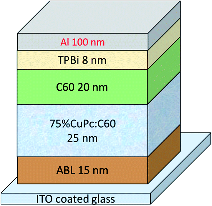 | ||
| Fig. 1 Device structure of organic solar cells, with CuPc, HPCzI, MoO3 and MoO3 doped HPCzI as anode buffer layer (ABL), respectively. | ||
Fig. 2a depicts the J–V characteristics of the best OPV devices. The device performance data deduced from the J–V characteristics are listed in Table 1, with shunt resistance (Rsh) and series resistance (Rs) included.31 Among the three devices with pure material (i.e., CuPc, HPCzI, and MoO3) as ABL, HPCzI device has the highest PCE of 1.62%, showing the potential of HPCzI as ABL in OPV devices. Since VOC is mainly determined by the energy level difference between HOMO of the donor and LUMO of the acceptor;32 and all our devices are based on the same donor–acceptor system, they show similar VOC. While the slight differences in VOCs still exist and agree well with the values of Rs. The relatively large Rs of the MoO3 device could be caused by the unsatisfied film formation of MoO3, e.g., rough surface, pin hole and overshoot,33 which may induce bad morphologies of the next active-layer. The decreased VOC of MoO3 device can be ascribed to a inhomogeneous surface.34 For devices with MoO3 doped HPCzI as ABL, when doping concentration was 25%, best performance was achieved, with the Jsc = 6.63 mA cm−2, VOC = 0.49 V, FF = 53%, PCE = 1.71%.
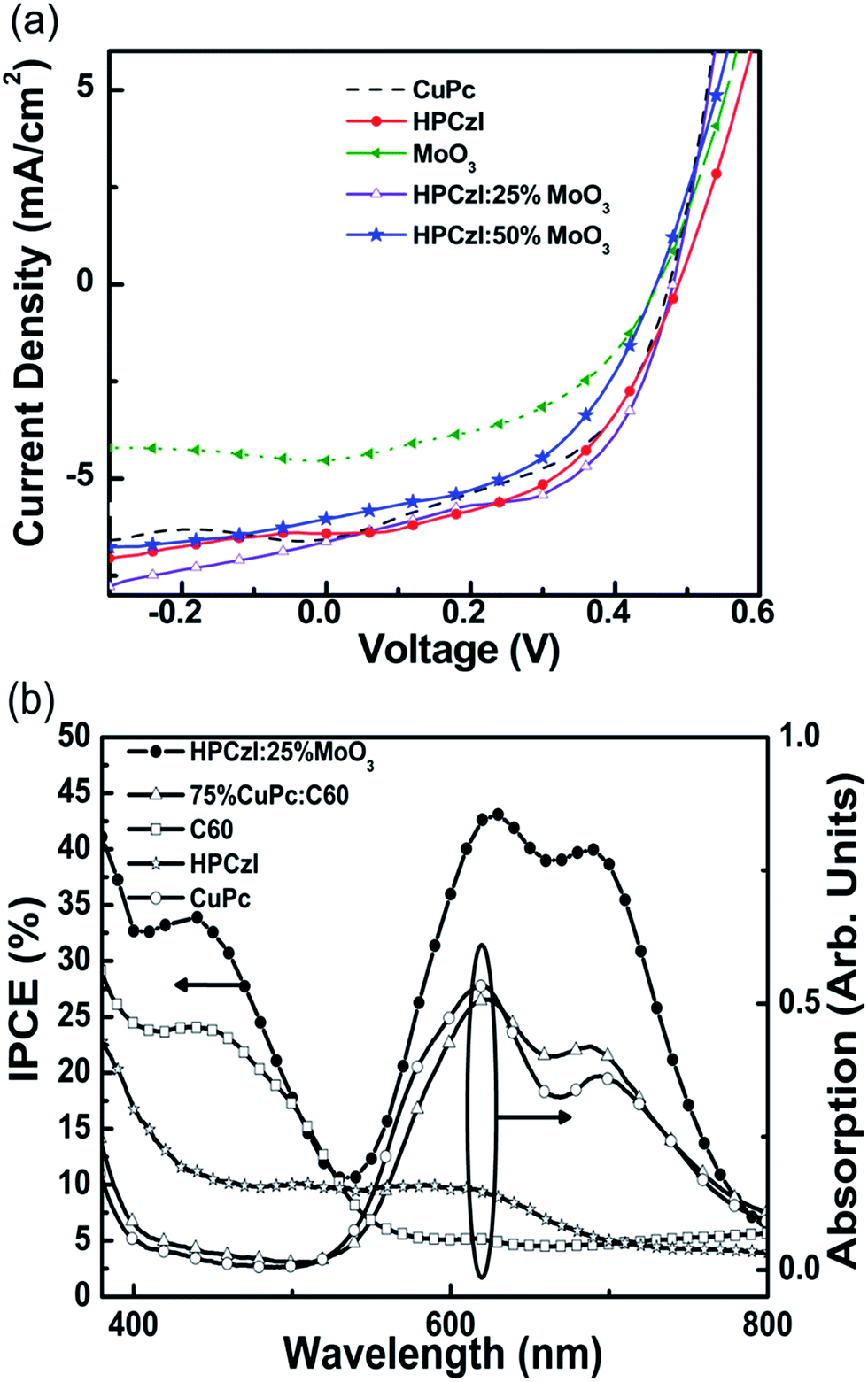 | ||
| Fig. 2 (a) J–V curves for devices with CuPc, HPCzI, MoO3 and HPCzI: Y% MoO3 as anode buffers, Y = 25, 50. (b) The IPCE of device with structure of ITO/HPCzI: 25% MoO3 (15 nm)/75% CuPc:C60 (25 nm)/C60 (20 nm)/TPBi (8 nm)/Al (100 nm), and the film absorptions of C60, HPCzI, CuPc and CuPc:C60 (3:1). | ||
| Anode buffer | Jsc (mA cm−2) | VOC (V) | PCE (%) | FF (%) | Rs (Ω) | Rsh (Ω) |
|---|---|---|---|---|---|---|
| CuPc | 6.56 | 0.47 | 1.48 | 48 | 20 | 190 |
| HPCzI | 6.22 | 0.49 | 1.62 | 53 | 23 | 267 |
| MoO3 | 4.58 | 0.47 | 0.97 | 45 | 30 | 133 |
| HPCzI:25% MoO3 | 6.63 | 0.49 | 1.71 | 53 | 15 | 222 |
| HPCzI:50% MoO3 | 6.01 | 0.47 | 1.37 | 49 | 22 | 181 |
Fig. 2b shows IPCE of the 25% MoO3 doped HPCzI device and the film absorption spectrum for the active layer (75% CuPc:C60 film) of this device, as well as the absorption curves for HPCzI, C60 and CuPc films. In the absorption spectrum of 75% CuPc:C60 blend film, there are only peaks at 620–693 nm, showing discrepancy with the IPCE curve which presents peaks both at 400–500 nm and 620–693 nm regions. This can be understood by examining the device structure and the absorption of C60 film. In this device above the active layer, there is an additional layer of C60 (20 nm) functioning as cathode buffer.30 As can be seen from Fig. 2b, the C60 film presents an absorption peak at 400–500 nm, which contribute mainly to the IPCE response at this region. Based on this IPCE curve, the theoretical Jsc can be calculated as 6.09 mA cm−2, which is slightly smaller than the value of 6.63 mA cm−2 by J–V curve. The difference between integrated photocurrent and measured photocurrent may result from the mismatch between the simulated light and the AM 1.5G spectra.
To investigate the working principles of HPCzI as ABL in OPV device, we studied its electronic structure by cyclic voltammogram (CV) along with UV-visible absorption spectra, and the results are shown in Fig. 3. The CV curve of HPCzI shows a well reversible redox wave for oxidation, which indicates excellent electrochemical stability for hole injection and transport, beneficial to its usage as ABL in OPV devices. The oxidation potential (EOX), determined as the mean value between the anodic current peak voltage and its corresponding cathodic peak, is 0.33 V (vs. Ag/AgCl). Based on this, the HOMO was obtained using the equation:35–39 EHOMO = −4.72 eV − EOX = −5.05 eV, while LUMOs were obtained via HOMO plus the energy gap of the absorption cutoff from absorption spectra, i.e., ELUMO = EHOMO + 2.90 eV = −2.15 eV. These HOMO and LUMO values agree well with those obtained by UPS in our previous study.29
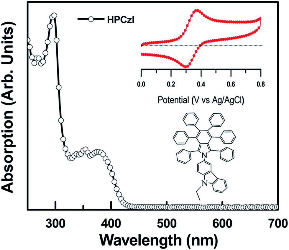 | ||
| Fig. 3 Absorption, CV curve, and molecular structure of HPCzI. | ||
According to the literature, the work function of ITO is 4.70 eV,40 and the HOMO/LUMO of CuPc and MoO3 are −5.20 eV/−3.50 eV and −5.30 eV/−2.30 eV, respectively.41,42 In OPV devices, after dissociation of photo-excited excitons in the active-layer, holes transport from CuPc in the active-layer passing the ABL, then reach the ITO anode. The routes for hole collection can be schematically shown in Fig. 4. With HPCzI as ABL, the hole collection barriers at active-layer/ABL and ABL/ITO are −0.1 and −0.4 eV; while those are 0.0 and −0.5 eV for devices with CuPc as ABL; 0.1 and −0.6 eV for device with MoO3 as ABL. In terms of energy barrier, CuPc ABL has no additional effect since the active-layer also contains CuPc; HPCzI ABL serves as energy-flattering step; while MoO3 ABL introduces hole collection barrier of 0.1 eV. The introduced hole barrier by MoO3 ABL may reduce hole collection efficiency. Compared to devices with CuPc ABL, the energetically positive location of HPCzI HOMO above CuPc can ensure facile hole extraction and less charge recombination. Therefore, cells with HPCzI anode buffer collect holes effectively and this indicates that HPCzI may serve as a better ABL compared to CuPc and MoO3 ABLs.
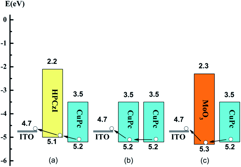 | ||
| Fig. 4 Hole collection in devices with different ABL: (a) HPCzI, (b) CuPc, (c) MoO3. | ||
To further investigate the mechanism for the improvement of device with HPCzI ABL, a series of hole-only devices were fabricated with the structure of ITO/NPB (10 nm)/X (60 nm)/NPB (100 nm)/Al, where X are pure films of CuPc, HPCzI, MoO3 and MoO3 doped HPCzI films, respectively. The NPB layer contacting with ITO plays a role of hole injection and circumvents the influence of the studied films contacting with ITO directly. The NPB layer before Al blocks electron injection as well as prevents device leak-current. This was especially important for a MoO3 film. We found that after the pure MoO3 film deposition, if the following NPB layer was not thick enough, the device often suffered from short circuit. Fig. 5 shows the J–V characteristics of these hole-only devices. As can be seen, there exist significant differences in the hole transport properties of these films, and 50% MoO3 doped HPCzI film exhibits the highest values.
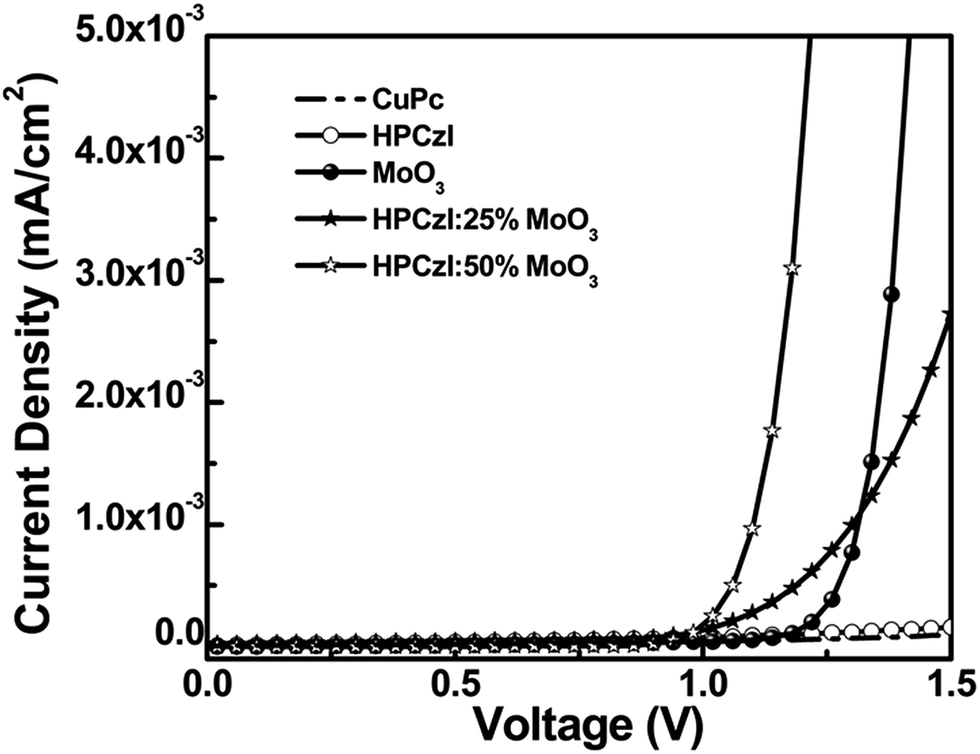 | ||
| Fig. 5 The J–V characteristics of hole-only devices with structure of ITO/NPB (10 nm)/X (60 nm)/NPB (100 nm)/Al (100 nm). The X are pure films of CuPc, HPCzI, MoO3 and MoO3 doped HPCzI films. | ||
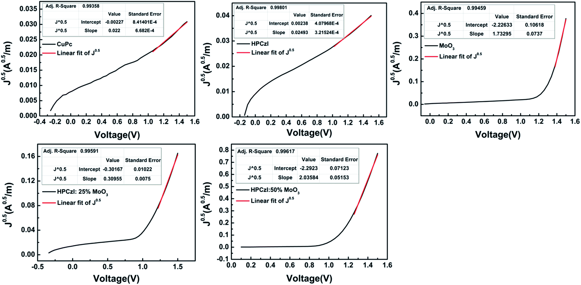 | ||
| Fig. 6 The plots of square root of J versus the voltage for the hole-only devices. The red lines are fit to the SCLC behaviour. | ||
The hole mobilities of the films can be extracted from these J–V curves at large voltage, where the current is limited by the space charge accumulation and can be described by Mott–Gurney's space charge limited current (SCLC) model,
 | (1) |
Taking the square root form of eqn (1), we got,
 | (2) |
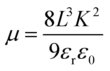
Drawing J0.5–V curves, and fitting the SCLC regime (shown as red lines in Fig. 6), slopes (K) of each curve can be obtained. Then, based on eqn (2), the hole mobility can be calculated according to eqn (3):
 | (3) |
Since these hole-only devices contain organic layers other than the concerned ABL, the mobility values cannot exactly represent those of the corresponding ABL. However, with the similar device structures, for the hole-conduction comparison among these ABLs, these are adequate. These data are shown in Table 2. It was found that the hole mobility of the HPCzI film was slightly higher than the CuPc film. However, the OPV device with ABL of CuPc showed smaller Rs. This contradictory result may come from the better interfacial property when CuPc was used as ABL for active-layer containing the same component of CuPc. Nevertheless, the HPCzI device gave better PCE, which agrees with the larger FF resulting from its larger Rsh (see Table 1). The film comprising a pure layer of MoO3 showed an even higher value of hole mobility which turned out to be three or four order of magnitude higher than that of CuPc and HPCzI films. However, pure MoO3 based OPV device presented the poorest PCE with high Rs and low Rsh. This may be due to rough surface morphology of MoO3 with overshoots,33 causing bad interface between the MoO3 and the active-layer, hence leading to high Rs and low Rsh. Furthermore, when doping MoO3 into HPCzI, compared with pure HPCzI device, hole mobility significantly increased. Although the 50% MoO3 doped HPCzI possesses the highest mobility, its OPV device is not the best. More MoO3 doped in HPCzI may cause worse film morphology, hence deteriorating device interface. As a result, the device with HPCzI containing 25% MoO3 as ABL shows the best performance.
Conclusions
In summary, we fabricated CuPc:C60 OPV devices with CuPc, HPCzI and MoO3 as ABLs. In the case of pure HPCzI, larger FF than CuPc and higher Jsc than MoO3 were obtained, due to its lower leakage current and improved interface, respectively. Through energy level analysis, the HOMO level of HPCzI provided satisfactory energy alignment, which may lead to efficient hole extraction and reduced charge recombination. For further improvement, devices with MoO3 doped HPCzI as ABL were fabricated. Study of the hole-only devices of the four ABLs material/composition indicates that the hole mobility of the MoO3 doped HPCzI devices is three or four order of magnitude higher than that for pure CuPc and pure HPCzI devices. However, the device performance decreased dramatically with the MoO3 concentration increased to 50%, which might be mainly due to the worse film morphology caused by more MoO3 composition. Therefore, the device with 25% MoO3 doped HPCzI as ABL showed the most highly performance.Acknowledgements
This work was financially supported by the National Natural Science Foundation of China (No. 61474064, 61504063, 61605076), Natural Science Foundation of Jiangsu Province (No. BK20150836), Nanjing University of Posts and Telecommunications (No. NY212076, NY212050, NY214177), National Basic Research Program of China 973 Program (2015CB932200), the Priority Academic Program Development of Jiangsu Higher Education Institutions (PAPD: YX03001), the Synergistic Innovation Center for Organic Electronics & Information Displays, and Jiangsu National Synergetic Innovation Center for Advanced Materials (SICAM).References
- H. E. Unalan, P. Hiralal, D. Kuo, B. Parekh, G. Amaratunga and M. Chhowalla, J. Mater. Chem., 2008, 18, 5909 RSC.
- B. Song and S. R. Forrest, Nano Lett., 2016, 16, 3905 CrossRef CAS PubMed.
- S. Li, L. Ye, W. Zhao, S. Zhang, S. Mukherjee, H. Ade and J. Hou, Adv. Mater., 2016, 28, 9423 CrossRef CAS PubMed.
- J. Zhao, Y. Li, G. Yang, K. Jiang, H. Lin, H. Ade, W. Ma and H. Yan, Nat. Energy, 2016, 1, 15027 CrossRef CAS.
- L. Yang, S. Zhang, C. He, J. Zhang, H. Yao, Y. Yang, Y. Zhang, W. Zhao and J. Hou, J. Am. Chem. Soc., 2017, 139, 1958 CrossRef CAS PubMed.
- S. D. Collins, N. A. Ran, M. C. Heiber and T. Q. Nguyen, Adv. Energy Mater., 2017, 7, 1602242 CrossRef.
- B. Kan, M. Li, Q. Zhang, F. Liu, X. Wan, Y. Wang, W. Ni, G. Long, X. Yang and H. Feng, J. Am. Chem. Soc., 2015, 137, 3886 CrossRef CAS PubMed.
- B. Kan, Q. Zhang, M. Li, X. Wan, W. Ni, G. Long, Y. Wang, X. Yang, H. Feng and Y. Chen, J. Am. Chem. Soc., 2014, 136, 15529 CrossRef CAS PubMed.
- A. W. Hains, J. Liu, A. B. F. Martinson, M. D. Irwin and T. J. Marks, Adv. Funct. Mater., 2010, 20, 595 CrossRef CAS.
- R. Steim, F. R. Kogler and C. J. Brabec, J. Mater. Chem., 2010, 20, 2499 RSC.
- L. M. Chen, Z. Xu, Z. Hong and Y. Yang, J. Mater. Chem., 2010, 20, 2575 RSC.
- H. Ma, H. L. Yip, F. Huang and A. K. Y. Jen, Adv. Funct. Mater., 2010, 20, 1371 CrossRef CAS.
- J. Wang, T. Wang, D. Cao, X. Zhao, J. Liu, M. Zhuo, B. X. Mi and Z. Q. Gao, Org. Electron., 2015, 23, 11 CrossRef CAS.
- M. T. Lloyd, C. H. Peters, A. Garcia, I. V. Kauvar, J. J. Berry, M. O. Reese, M. D. Mcgehee, D. S. Ginley and D. C. Olson, Sol. Energy Mater. Sol. Cells, 2011, 95, 1382 CrossRef CAS.
- H. Zhou, Y. Zhang, C. K. Mai, S. D. Collins, T. Q. Nguyen, G. C. Bazan and A. J. Heeger, Adv. Mater., 2014, 26, 780 CrossRef CAS PubMed.
- C. E. Petoukhoff, D. K. Vijapurapu and D. M. O'Carroll, Sol. Energy Mater. Sol. Cells, 2014, 120, 572 CrossRef CAS.
- Y. D. Liu, B. Chu, Z. S. Su, W. L. Li, T. J. Zhuang, F. M. Jin, X. W. Yan, B. Zhao, F. Zhang and D. Fan, Org. Electron., 2012, 13, 2865 CrossRef CAS.
- A. Godoy, L. Cattin, L. Toumi, F. Diaz, M. Del Valle, G. Soto, B. Kouskoussa, M. Morsli, K. Benchouk and A. Khelil, Sol. Energy Mater. Sol. Cells, 2010, 94, 648 CrossRef CAS.
- H. P. Kim, S. J. Lee, A. R. bin Mohd Yusoff and J. Jang, RSC Adv., 2016, 6, 28599 RSC.
- C.-H. Chang and S.-A. Chen, Appl. Phys. Lett., 2007, 91, 103514 CrossRef.
- F. A. S. Lima, M. J. Beliatis, B. Roth, T. R. Andersen, A. Bortoti, Y. Reyna, E. Castro, I. F. Vasconcelos, S. A. Gevorgyan and F. C. Krebs, APL Mater., 2016, 4, 026104 CrossRef.
- W. J. Dong, G. H. Jung and J.-L. Lee, Sol. Energy Mater. Sol. Cells, 2013, 116, 94 CrossRef CAS.
- T. Zhuang, T. Sano and J. Kido, Org. Electron., 2015, 26, 415 CrossRef CAS.
- K. X. Steirer, J. P. Chesin, N. E. Widjonarko, J. J. Berry, A. Miedaner, D. S. Ginley and D. C. Olson, Org. Electron., 2010, 11, 1414 CrossRef CAS.
- H. Choi, B. Kim, M. J. Ko, D.-K. Lee, H. Kim, S. H. Kim and K. Kim, Org. Electron., 2012, 13, 959 CrossRef CAS.
- M.-H. Choi, E. J. Lee, J. P. Han and D. K. Moon, Sol. Energy Mater. Sol. Cells, 2016, 155, 243 CrossRef CAS.
- J. Subbiah, D. Y. Kim, M. Hartel and F. So, Appl. Phys. Lett., 2010, 96, 27 CrossRef.
- P. Zhang, X. Xu, Y. Dang, S. Huang, X. Chen, B. Kang and S. R. P. Silva, ACS Sustainable Chem. Eng., 2016, 4, 6473 CrossRef CAS.
- B.-X. Mi, P.-F. Wang, M.-W. Liu, H.-L. Kwong, N.-B. Wong, C.-S. Lee and S.-T. Lee, Chem. Mater., 2003, 15, 3148 CrossRef CAS.
- X. Li, Y. Chen, J. Sang, B.-X. Mi, D.-H. Mu, Z.-G. Li, H. Zhang, Z.-Q. Gao and W. Huang, Org. Electron., 2013, 14, 250 CrossRef CAS.
- M.-S. Kim, B.-G. Kim and J. Kim, ACS Appl. Mater. Interfaces, 2009, 1, 1264 CAS.
- S. Cho, L. Piper, A. DeMasi, A. Preston, K. Smith, K. Chauhan, P. Sullivan, R. Hatton and T. S. Jones, J. Phys. Chem. C, 2010, 114, 1928 CAS.
- A. Arfaoui, S. Touihri, A. Mhamdi, A. Labidi and T. Manoubi, Appl. Surf. Sci., 2015, 357, 1089 CrossRef CAS.
- M. D. Irwin, J. D. Servaites, D. B. Buchholz, B. J. Leever, J. Liu, J. D. Emery, M. Zhang, J. H. Song, M. F. Durstock and A. J. Freeman, Chem. Mater., 2011, 23, 2218 CrossRef CAS.
- Z. Q. Gao, B. X. Mi, G. Z. Xu, Y. Q. Wan, M. L. Gong, K. W. Cheah and C. H. Chen, Chem. Commun., 2007, 46, 117 Search PubMed.
- M. R. Andersson, M. Berggren, O. Inganäs, G. Gustafsson, J. Gustafsson-Carlberg, D. Selse, T. Hjertberg and O. Wennerström, Macromolecules, 1995, 28, 7525 CrossRef CAS.
- B. W. D'Andrade, S. Datta, S. R. Forrest, P. Djurovich, E. Polikarpov and M. E. Thompson, Org. Electron., 2005, 6, 11 CrossRef.
- A. K. Agrawal and S. A. Jenekhe, Chem. Mater., 1996, 8, 579 CrossRef CAS.
- I. Seguy, P. Jolinat, P. Destruel, J. Farenc, R. Mamy, H. Bock, J. Ip and T. Nguyen, J. Appl. Phys., 2001, 89, 5442 CrossRef CAS.
- J. Park, H. M. Kim, D. W. Kim and J. S. Choi, Appl. Phys. Lett., 2010, 97, 191 Search PubMed.
- C. W. Chu, V. Shrotriya, G. Li and Y. Yang, Appl. Phys. Lett., 2006, 88, 183 Search PubMed.
- S. Fengler, T. Dittrich and M. Rusu, J. Appl. Phys., 2015, 118, 183 CrossRef.
- N. Shi and R. Ramprasad, Appl. Phys. Lett., 2006, 89, 102904 CrossRef.
- T. Y. Chu and O. Song, Appl. Phys. Lett., 2007, 90, 151 Search PubMed.
- J. Simmons and G. Nadkarni, J. Vac. Sci. Technol., 1969, 6, 12 CrossRef.
| This journal is © The Royal Society of Chemistry 2017 |