
 Open Access Article
 This Open Access Article is licensed under a
 Creative Commons Attribution 3.0 Unported Licence
Enhanced polarization and dielectricity in BaTiO3:NiO nanocomposite films modulated by the microstructure†
M. J. Chen,
X. K. Ning *,
S. F. Wang* and
G. S. Fu
*,
S. F. Wang* and
G. S. Fu
Hebei Key Lab of Optic-electronic Information and Materials, The College of Physical Science and Technology, Hebei University, 180 Wusi Road, Baoding 071000, China. E-mail: xkning@alum.imr.ac.cn; sfwang@hbu.edu.cn
First published on 3rd August 2017
Abstract
Parallel and vertical interfaces in vertically and parallelly aligned nanocomposite thin films have been shown to be an effective method to manipulate functionalities. However, tuning the physical properties by modulating the microstructure of the self-assembled nanocomposite films and understanding the physical properties underlying the manipulation is still a challenge. In this work, BaTiO3:NiO (BTO:NiO) nanocomposite films with nanomultilayer, nanocolumnar and nanogranular structures have been prepared on Nb:SrTiO3 (Nb:STO) substrates by a pulsed laser deposition (PLD) method. These films have been used as a model system to investigate the relationship between the microstructure and the ferroelectric properties. The polarization, dielectricity and leakage can be separately modulated by tuning the microstructures. The experimental results show that the remanent polarization of the nanocomposite films is much higher than that of the pure BTO films. By precisely modulating the microstructure, a significantly enhanced polarization (>70% higher than pure BTO for the nanomultilayer structure) and dielectricity (>60% and >240% higher than pure BTO for the nanomultilayer and nanocolumnar structure, respectively) are realized in these films. These results demonstrate that tunable ferroelectric properties can be realized by controlling the microstructures in the epitaxial BTO:NiO nanocomposite thin films, which will be expected to be applied in the devices such as supercapacitors, solar cells and non-volatile memory applications.
Introduction
Artificially layered and self-assembled nanocomposites, in which two phases grow epitaxially with each other, provide many opportunities to develop systems with novel and enhanced functionalities.1,2 These materials have shown tremendous potential in technological applications in recent years because of their potential application in next-generation technological devices, for instance, non-volatile random access memories (RAM),3 tunnel junctions,4 and photocatalysis as well as energy conversion.5,6 The properties of these nanostructures depend significantly on nanostructure morphology as well as orientation.7–9 Especially, functional properties of these nanocomposite films, such as low-field magnetoresistance (LFMR),10,11 magnetoelectric properties,12,13 electronic-transport properties,14,15 ferroelectric (FE) properties16,17 and dielectric properties18 tremendously depend on the size, shape, and arrangement of each constituted phase in these composite films. Therefore, manipulation of the micro-structures of nanocomposite films can be expected to give rise to rich tunable functionalities.As far as FE nanocomposites are concerned, due to the possibilities for applications that include supercapacitors as well as the increased storage densities for the FE random storage,19,20 the perovskite FE oxides (e.g., Pb(ZrTi)O3, BaTiO3, and BiFeO3) have to date been the most popular materials to synthesis of nanocomposite films with highly controllable microstructure. Recently, remarkable improvement in oxide thin-film techniques have allowed for the growth and characterization of FE heterostructures with (near) atomic precision, opening an avenue for the fabrication of the nanocomposite films with different microstructures. The highly ordered nanocomposite FE films show enhanced polarization and dielectric properties, leading to the rapidly development of the research in the field of FE-RAM devices.
Up to now, due to the deepening cognition of the intrinsic and extrinsic polarization, dielectric and FE nanodomain, growing attention has been paid to BaTiO3 (BTO) FE nanocomposite films. In these nanocomposite films, microstructures with nanogranular, nanomultilayer and nanocolumnar characteristics according to the distribution and arrangement of the second phase have been well studied. For example, firstly, artificial BTO nanocomposites films with the nanomultilayer configuration have drawn considerable attention due to a remarkable enhancement in polarization and resistivity. Unusual ferroelectricity in this structure is expected to be used in the preparation of high-performance microelectronic devices.21,22 In 1994, Tabata et al. have firstly synthetized BTO/SrTiO3 (BTO/STO) nanocomposites films with nanomultilayer structure by Pusled Laser Deposition (PLD), in which BTO and STO formed layered structure and epitaxially grown with each other.23 Lee et al. fabricated a series of CaTiO3/BTO/STO superlattices, and found an enhancement in the FE properties with respect to pure BTO films.24 In charge- or orbital-mediated artificial layered structure of the BTO/Pb(Zr0.52Ti0.48)O3 (BTO/PZT) and BTO/LaNiO3, the interfacial charge carrier density modulated by polarization charge determined the functional properties. For the nanomultilayer structure, the polarization properties could be improved as compared with the pure films, due to the preserving full strain and combining heterointerfacial couplings.23–26 In addition, oxygen vacancy accumulation as well as the charge transfer at the interface for the nanomultilayer structure also plays an important role in inducing the local polarization enhancement.27 Secondly, BTO based naonocomposite thin films with nanogranular configuration also produced a tremendous flurry of research interest because of their unique physical and chemical properties. Ge et al. have shown that the Co and Ni nanocrystals in the face-center cubic structure dispersed well in the single BTO matrix.28,29 Their results provide an effective way to engineer BTO/Ni or BTO/Co nanocomposite films with desired qualities. Metal-BTO nanocomposite films, such as BTO/Ag, BTO/Co and PbTiO3/Pb (PTO/Pb) composite films, have showed enhanced optical and electrical properties.30–32 For the nanogranular structure, the embedded nanoparticles lead to the coarsening and coalescence of crystal grains of the FE films and improve the polarization properties for the nanogranular structure.28,30 The permittivity and tunability in this structure also been tuned by conductive nanoparticles as the field-induced permittivity was estimated for different volume fraction of conductive particles.30,33 Thirdly, BTO based naonocomposite thin films with nanocolumnar structure have also been studied extensively as the enhanced dielectric properties. Vertical interfaces in vertically aligned nanocomposite thin films have been approved to be an effective method to manipulate functionalities. Zheng et al. have studied the BTO:CoFe2O4 (BTO:CFO) nanocomposite films with the nanocolumnar structure to explore the ferroelectromagnets. Thermodynamic analyses show that the magnetoelectric coupling in such a nanostructure can be understood on the basis of the strong elastic interactions between the two phases.34 Lee et al. have created a nanoscaffold Ba0.6Sr0.4TiO3:Sm2O3 (BSTO:SmO) composite films with nanocolumnar structure which have a very high tunability which scales inversely with loss.35 In addition, (BTO)1−x:(SmO)x thin films with nanocolumnar configuration show a dielectric relaxation behavior due to the sinks to attract oxygen vacancies at the vertical interfaces.18 For the nanocolumnar structure, the large vertical strain and strong elastic interactions could lead to the enhancement for the polarization and permittivity.34,35
However, on the one hand, the reported enhancement of dielectric for BTO based naocompsoites films with nanomultilayer structure is still too slight compared with the pure films. For the nanogranular structure, most of these studies have just focused on the dielectric or optical properties of these nanocomposite thin films, very little has been done to understand the polarization properties as they are too conducting for application of macroscopic electric fields. What's more, very weak polarization properties have been measured for the nanocolumnar structure which hinder the application for polarization-controllable functional devices. On the other hand, the microstructure plays the key role in determining the electrical properties for the BTO based nanocomposite films. Experimental studies on controlling the microstructure of the composite films are usually carried out by changing the volume fraction of the second phase. However, interestingly, extreme enhancement of the functionalities always appears in the vicinity of one critical content of the second phase which correlates with the transformation of the microstructures.7,10,36 Therefore, the tuning of the microstructures of the nanocomposite films at a critical content of the second phase could help us to tailor their desirable functionalities.
In this study, the NiO, which is economical, eco-friendly, stability, lattice-matching with BTO and owns unique properties at nanometer sizes, has been used to prepare BTO nanocomposite thin films by PLD method. Of the transition-metal monoxides, NiO has received by far the greatest amount of attention, prompted by a remarkable range of motivations.37 The values of the dielectric constant of NiO have a weak temperature dependence which is important for the stability of the device.38 It is noted that NiO has been one of the most promising candidates because it has a high melting point and exhibits the highest increase in the dielectric constant compared to other metal monoxides for the BTO FE materials.39,40 What's more, as compared to their corresponding counterparts epitaxially grown on the substrates, the type of the perovskite titanate and structure is one of the most important issues to modulated the FE properties.41 In the bulk composites, the addition of NiO was more effective in broadening dielectric constant peaks and values.42,43 For the BTO:NiO composties, the switching polarities for the two semiconductors are opposite to each other and the interdiffusion between the BTO grains and NiO can affect the rather complex dielectric dispersion and conductivity spectra.44,45 Hence, the enhanced polarization and dielectric constant may be realized by controlling the geometry structures of NiO with BTO in the BTO:NiO nanocomposite thin films. The experimental results show that the remanent polarization, leakage and dielectric constant, can be well modulated by tuning the NiO fraction and the microstructure.
Experimental
Synthesis of the films
BTO:NiO nanocomposite thin films with a thickness of 120–180 nm were grown on Nb-doped SrTiO3 single-crystal (Nb:SrTiO3 with 0.7 wt% of Nb, abbreviated as Nb:STO) (001) substrates by PLD using a XeCl (λ = 308 nm) excimer laser. The laser flux is approximately 1.2 J cm−2 with a repetition rate of 2 Hz. BTO and NiO thin films were deposited on Nb:STO substrates at 0.2 mbar pressure of pure O2 at a substrate temperature of 630 °C. The distance between the target and the substrate was 35 mm. Prior to deposition, the substrates were ultrasonically cleaned with acetone followed by ethanol. The chamber was evacuated using a turbo-pump down to about 2 do10−5 Pa to remove any extraneous particles. The samples were finally annealed at a pressure of 0.5 bar of pure O2 to remove oxygen vacancies (deposition parameters and their levels see Table S1†). For fabricating the composite films with different geometry microstructures with the same NiO ratios, the composite (BTO)0.9:(NiO)0.1 and (BTO)0.8:(NiO)0.2 targets and two single BTO and NiO targets have been used. The (BTO)0.9:(NiO)0.1 and (BTO)0.8:(NiO)0.2 ceramic target were made by BTO, and NiO powders (99.99%) in proper ratios and following multiple steps of standard solid state reaction processes. The single BTO and NiO targets are directly synthetized by BTO and NiO powder (99.99%), respectively (targets parameters and their synthetized materials see Table S2†). In this paper, to produce the BTO:NiO nanocomposite films with the nanomultilayer and nanocolumnar structures, two separated targets of BTO and NiO were alternately used to deposit BTO and NiO on the Nb:STO substrate, as shown in Fig. 1(a) and (b). The preparation process can be expressed as a formula of [(BTO)t1/(NiO)t2]n, where, t1 and t2 are the deposition times for BTO and NiO, respectively, and n is their repeat number. These three important parameters, t1, t2, and n, were used to control the composition, thickness, and microstructure of the BTO:NiO nanocomposite films. First, we tune the microstructure for the NiO volume fractions of 10%, 20%, and 30%, where the deposition times were taken as t1 = 8–30 and t2 = 100 s, respectively, and the growth shows Frank–van der Merwe, or layer-by-layer growth behavior.46 When the seed layers of the BTO and NiO phases expand in two dimensions, a planar layer of the BTO and NiO phases will form, as shown in Fig. 1(a). The samples will hereafter be denoted as M-1, M-2 and M-3 with the NiO ratio about 10, 20% and 30% for the nanomultilayer configuration, respectively. The parameters for each sample are summarized in Table 1. To obtain a nanocolumnar microstructure, the deposition times for BTO and NiO are t1 = 1–3 s and t2 = 10 s. The targets have to be rotated sufficiently fast to ensure that BTO or NiO seed nuclei were not attached with each other to initiate an island-type growth mode (Volmer–Weber model) at an early stage, as shown in Fig. 1(b). The samples will hereafter be denoted as C-1, and C-2 with the NiO ratio about 10% and 20% for the nanocolumnar configuration, respectively. In our previous study,7 under this island-type growth mode, the deposited particles of BTO and NiO more strongly bond to their own phase and coherently build up the columnar configuration, as shown in Fig. 1(b). This is energetically favorable for the growth because the lattice mismatch and strain are decreased, giving rise to the formation of a nanocolumnar microstructure.7 For nanocomposite films with a nanogranular structure (the samples will be denoted as G-1 and G-2) have been deposited by using a single composite (BTO)0.9:(NiO)0.1 and (BTO)0.8:(NiO)0.2 target, as shown in Fig. 1(c).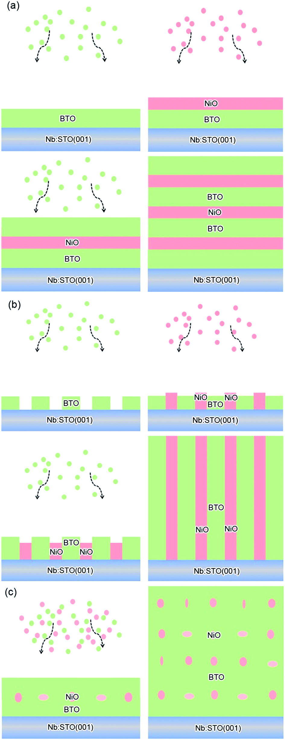 | ||
| Fig. 1 Schematic illustrations of the growth modes for the BTO:NiO nanocomposite films with equal volume fractions of BTO and NiO but with different microstructures: (a) nanocolumnar nanomultilayer configuration, (b) configuration and (c) nanogranular configuration. | ||
| Label | Samples | Target | t1 (s) | t2 (s) | n | d (nm) |
|---|---|---|---|---|---|---|
| M-1 | (BTO)0.9:(NiO)0.1 | BTO and NiO | 8 | 100 | 35 | 160 |
| M-2 | (BTO)0.8:(NiO)0.2 | BTO and NiO | 13 | 100 | 30 | 145 |
| M-3 | (BTO)0.7:(NiO)0.3 | BTO and NiO | 30 | 100 | 28 | 140 |
| C-1 | (BTO)0.9:(NiO)0.1 | BTO and NiO | 1.5 | 10 | 200 | 130 |
| C-2 | (BTO)0.8:(NiO)0.2 | BTO and NiO | 3 | 10 | 200 | 125 |
| G-1 | (BTO)0.9:(NiO)0.1 | (BTO)0.9:(NiO)0.1 | — | — | — | 130 |
| G-2 | (BTO)0.8:(NiO)0.2 | (BTO)0.8:(NiO)0.2 | — | — | — | 140 |
Apparatus
The crystal structure and orientation of the BTO:NiO films were analyzed by θ–2θ scans of X-ray diffraction (XRD, Rigaku RINT2000, Cu Kα radiation). Transmission electron microscopy (TEM) specimens for both cross-sectional and plan view observations were prepared by conventional method, i.e., by the standard procedure of cutting, gluing, slicing, grinding and finally ion milling with Ar+ ions until they were electron transparent. A Gatan precision ion polishing system (PIPS 695; Gatan) with a liquid–nitrogen-cooled stage was used to prevent the cross-sectional specimens from preferential thinning effects. Plan view specimens were milled only from the substrate side. The microstructures of the films were characterized by TEM (Tecnai G2 F20, accelerating voltage 200 kV). A Tecnai G2 F30 transmission electron microscope, equipped with a high-angle-annular-dark-field (HAADF) detector and a post-column Gatan (Titan Cubed 60–300 kV microscope (FEI) fitted with a high-brightness field emission gun (X-FEG) and double Cs correctors from CEOS, and a monochromator operating at 300 kV), was used for Z-contrast imaging analysis. The FE properties of the films were measured by using a standard FE testing system (TF2000E; Aixacct). The dielectric constant and loss were measured in a frequency range of 1–100 kHz using an impedance analyzer LCR Hitester (HIOKI 3532-50). The chemical valence of the ions in the BTO:NiO films were determined by X-ray photoelectron spectroscopy (XPS, Therma ESCALAB 250; Al Kα source, 1486.60 eV, resolution: 400 meV, energy step: 0.1 eV).Results and discussion
Fig. 2(a) shows XRD patterns of the (BTO)1−x:(NiO)x nanomultilayer films with different NiO ratios (x = 0.1, 0.2 and 0.3, abbreviated as M-1, M-2 and M-3, respectively). In all the samples, diffraction peaks of the BTO and NiO phases around the diffraction peaks of (002) planes for the Nb:STO substrate are observed, indicating that the BTO and NiO layers grown epitaxially on the Nb:STO (001) substrate. The epitaxial nature of the films is also confirmed by the TEM results presented later. Fig. 2(b) illustrates that, with increasing NiO content, the (002) reflection of BTO and the (200) reflection of NiO shift to higher angles. Based on these diffraction peaks, we can calculate the out-of-plane lattice parameters of the BTO and NiO layers in the nanomultilayer. The corresponding decrease of the lattice parameters of the BTO and NiO phases with increasing NiO fraction is depicted in Fig. 2(d). The BTO, epitaxially grown on the Nb:STO substrate, will experience in-plane compressive stress due to the lattice mismatch between BTO (a = 4.015 Å) and Nb:STO (a = 3.91 Å). Because of the presence of NiO (a = 4.172 Å), the BTO will experience tensile stress arising from the clamping constraints of the NiO. Conversely, the NiO will experience in-plane compressive stress arising from the clamping constraints of the BTO. Therefore, the lattice parameters of BTO decrease with increasing NiO content. Fig. 2(c) shows XRD patterns of the (BTO)1−y:(NiO)y nanocolumnar films and nanogranular films with different NiO concentration (y = 0.1, 0.2, abbreviated as C-1 and C-2 for the nanocolumnar films, respectively). G-2 is the nanogranular films with the NiO ratio about 20%. For the nanocolumnar films, as shown in Fig. 2(c), the (002) reflection of BTO and the (200) reflection of NiO shift to lower angles with increasing NiO content. The corresponding increase of the lattice parameters of the BTO phases with increasing NiO fraction is depicted in Fig. 2(d). Compared with the bulk value of BTO (a = 4.015 Å) and cubic NiO (a = 4.172 Å), the BTO and NiO is almost relaxed for the nanogranular composite films. It is noted that because of the presence of the vertical interfaces in the nanocolumnar films, the BTO will experience tensile stress arising from the clamping constraints of the surrounding NiO along the out-of-plane direction. Conversely, the NiO will experience out-of-plane compressive stress arising from the clamping constraints of the surrounding BTO. Therefore, the lattice parameters of BTO increase compared with the pure films.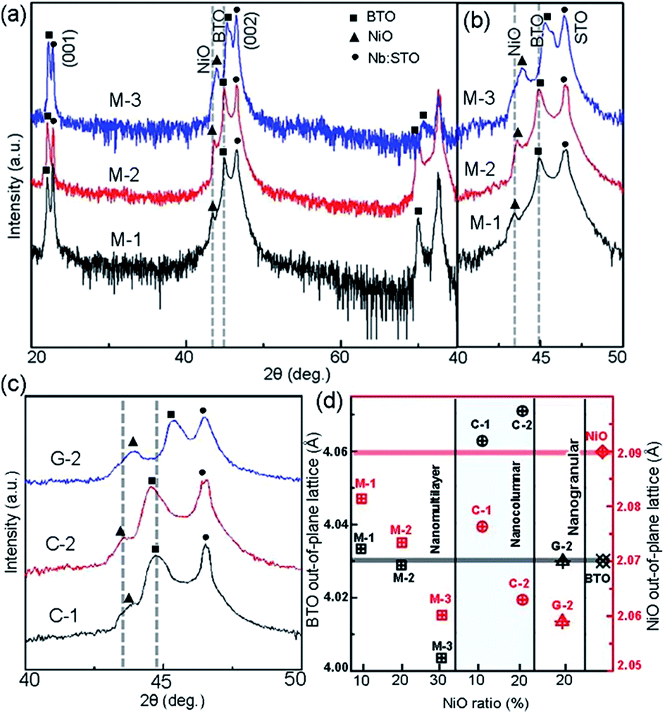 | ||
| Fig. 2 (a and b) XRD patterns of the BTO:NiO nanomultilayer with different NiO contents (left) and an enlarged XRD scan around the (002) diffractions of the samples. (c) Lattice parameters of the BTO and NiO as a function of the NiO fraction and microstructure. (d) The corresponding decrease of the lattice parameters of the BTO and NiO phases with increasing NiO fraction. | ||
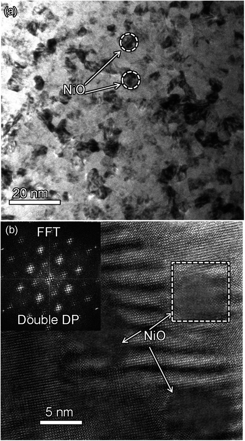
TEM study has been conducted to characterize the microstructures and the epitaxial nature of the composite films. The films prepared with the growth mode of Fig. 1(a) have formed nanomultilayer structures. Fig. 3(a) shows low-magnification TEM images for the M-2. The total thickness is about 145 nm, and the individual thickness for BTO and NiO layers is about 0.8 nm and 2 nm, respectively. It is clearly exhibited that the interface between the film and substrate in the samples is flat and sharp. NiO and BTO are two-phase separation forming a nanomultilayer structures along the out-of-plane direction. The HAADF micrograph in Fig. 3(b) reveals that the nanomultilayer exhibits perfect epitaxy. The sharp Z contrast across the interface indicates minimal interdiffusion at the interface, absence of any extended structural defects such as misfit dislocations or antiphase boundaries. Fig. 4 shows a vertical-view TEM images of the as-grown BTO:NiO films of the C-1 samples. The dotted line is the interfaces between the composite films and the Nb:STO substrates. At the composition of 0.1 for the NiO, a vertical columns at both the bottom and the top have been found. Fig. 4(b) and (c) show the high-resolution image of the NiO nanopillar (2–5 nm) within the BTO matrix. The spacing between them is about 5–10 nm. The typical HAADF micrographs of BTO–NiO columns have been conducted at the bottom and inner part of the C-1 sample, respectively. Fig. 4(b) and (c) demonstrate that the NiO nanopillar has very high epitaxial quality of these two phases and atomically sharp heterointerface between them. Also, STEM-EDX analysis (red dashed line in Fig. 4(b)) result confirms the alternating phase arrangement for the NiO in the BTO matrix (Fig. 4(d)). It can be observed that the NiO and BTO are separating into two phases and forming a columnar structure along the out-of-plane direction (indicated by the white dashed lines). This is because the radius of a Ni2+ ion (0.69 Å) is larger than that of Ti4+ ion (0.60 Å), and the larger Ni2+ ion enters into the lattice of BTO with difficulty and probably is being pushed out toward the phase boundary to release the local strain.47 It is noted that the self-assembled nanocolumnar structures formed for the C-1 samples, from their low magnification TEM image and the high-resolution TEM (HRTEM) image. However, for the C-2, as shown in Fig. S1,† some planar structure is found at the base of the film. In addition, the diameter of the nanocolumnar increased (∼5–10 nm) and the nanocolumnar become not so ordered compared with that in the C-1 samples (Fig. S1(b) and (d)†). To better understand the microstructures of such nanocolumnar structures, a plan-view TEM image of the C-2 sample also has been conducted. The corresponding low magnification TEM image shows clear rows of NiO pillars. It is obvious that self-assembled NiO nanocolumnar (in dark contrast) with an average diameter of 5–10 nm are uniformly distributed in the BTO matrix (in bright contrast), as shown in Fig. 5(a) and (b). In the fast Fourier transformation (FFT) patterns transformed from the HRTEM image (Fig. 5(b)), the second order reflection of the (100) and (001) planes can be clearly observed. Double-diffraction spots are visible around each of these primary reflections. The double diffraction is a common feature for two-phase materials exhibiting epitaxial or topotaxial properties.48 The films prepared with the growth mode of Fig. 1(c) have formed nanogranular structures. For G-1, the NiO nanoparticle are very fine (∼2 nm in diameter and the spacing between them is about 5 nm) (Fig. S2†). As the ratio of NiO increases, the density of NiO nanoparticle increases and the diameter is about 5–10 nm (Fig. S3†). The results obtained in this study are in line with those of the nanogranular microstructures in (Nd7/12Li1/4)TiO3 reported by Guiton et al.49 and in the decomposing deposited films of the ZnMnGaO4 reported by Ni et al.50 The XRD results and the corresponding HRTEM confirms the orientation relationships between BTO and NiO with the underlying STO substrate, i.e., (001)BTO//(002)NiO//(001)STO (out-of-plane) and (100)BTO//(200)NiO//(100)STO (in-plane). Based on the TEM results, typical depictions for the nanomultilayer, nanocolumnar, and nanogranular structure have been successfully prepared by tuning the growth mode, as shown in Fig. 1. The green part represents the BTO phase, while the pink part represents the NiO phase.
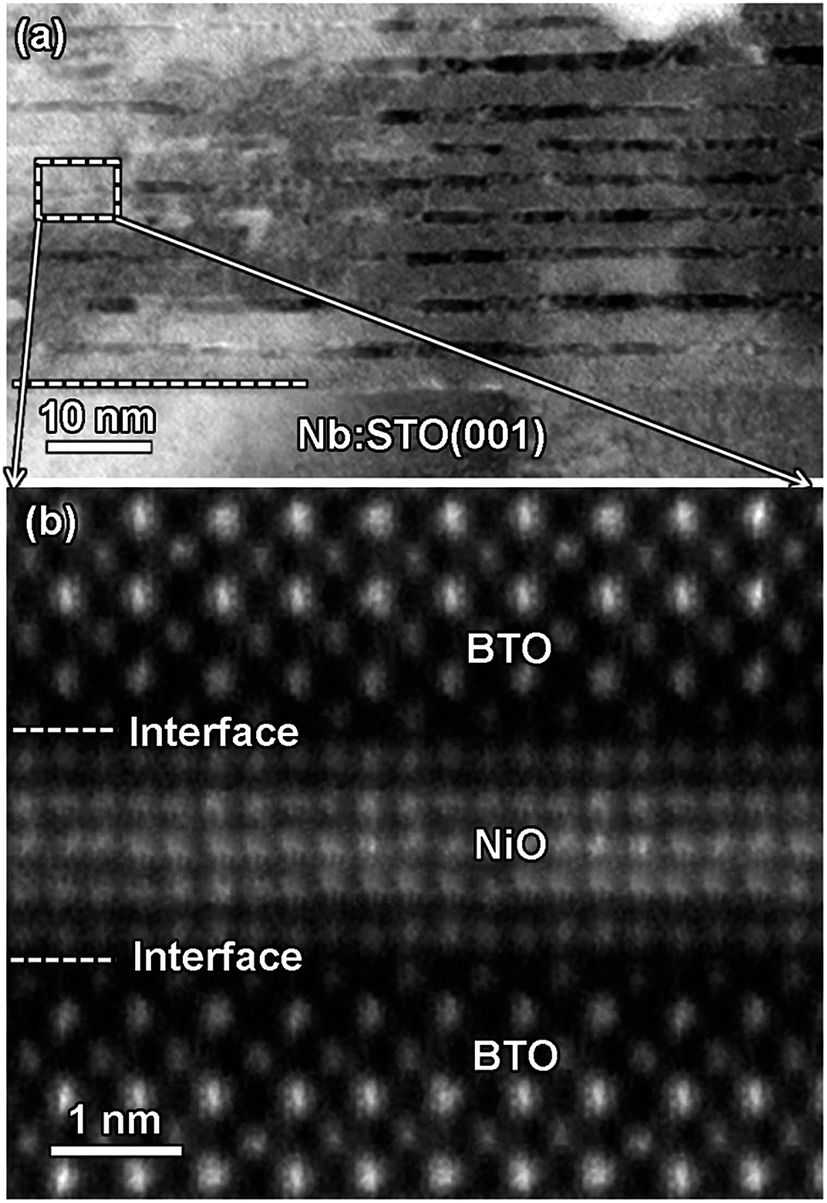 | ||
| Fig. 3 (a) A cross-sectional TEM image of the nanomultilayer film M-2. (b) The high-angle annular dark-field (HAADF) micrograph of the film for the M-2. | ||
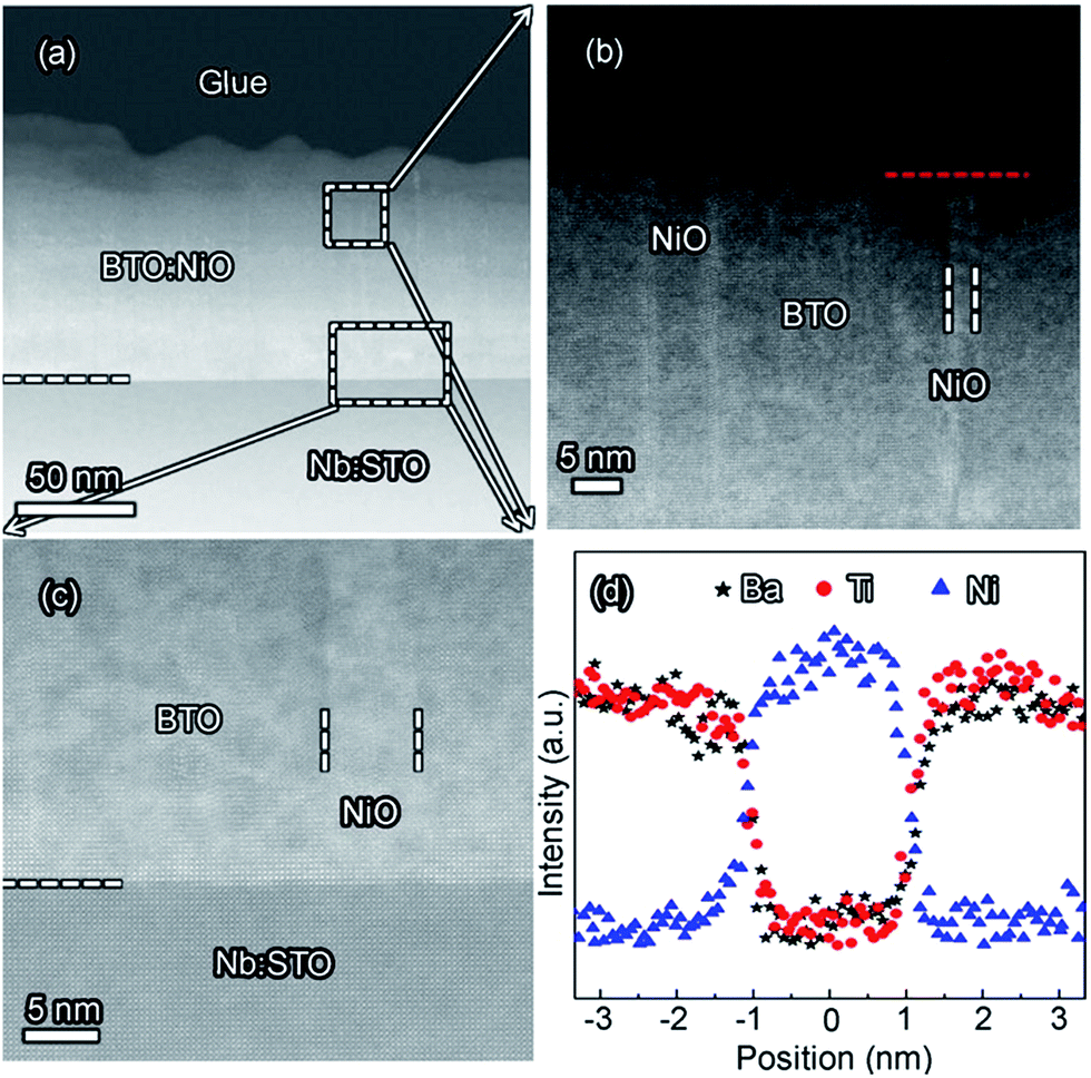 | ||
| Fig. 4 (a) A cross-sectional TEM image of the nanocolumnar film C-1. (b) and (c) HRTEM displaying the nanopillar NiO at the bottom and inner part of the films. The dotted line is the interfaces between the composite films and the Nb:STO substrates. (d) STEM-EDX line scans the region of red dashed line in (b). | ||
 | ||
| Fig. 5 (a) Plan-view TEM image of C-2 films with 20% NiO phase. It shows the NiO nanocolumnar in BTO matrix. (b) HRTEM image showing the vertical NiO nanocolumnar structure in BTO phase. | ||
To further understand how the microstructures influence the functionalities of the composite films, the electric properties were investigated. Fig. 6(a) shows the FE polarization–electric field (P–E) hysteresis loops of the BTO:NiO nanomultilayer films with different NiO ratios. The switching frequency is 1 kHz and the maximum applied voltage is 20 V. From the well-defined P–E loops, we can rule out the extrinsic FE polarization. An interesting phenomenon is that the P–E loops show a symmetric polarization switching behavior with a weaker imprint effect (the horizontal shift of the FE hysteresis loops). The imprint effect means the presence of the built-in-electric field in FE films. It is noted that in the BTO:NiO nanocomposite films, there are almost not a built-in electric field for the different microstructures, which is quite different from the previous reports that showed a large imprint in the FE superlattices.51,52 Fig. 6(a) shows that the polarization properties of multilayer are sensitive to the thickness of the NiO. Compared to the pure BTO thin films, the remanent polarization (Pr) of the M-1 samples reaches above 24 μC cm−2 which increased by almost 71% by the addition of the NiO ultra-thin layers. However, the loops of M-2 become very slim and tilted compared with the M-1 samples. There is no loop for the thicker NiO layer of the M-3 films. For the nanocolumnar structure, as shown in Fig. 6(b), it can be seen that the Pr and Ps remarkably increase with increasing the NiO ratio. The Pr value for the C-1 was 26 μC cm−2. These values were found to be greatly enhanced in comparison with the value of 14 μC cm−2 for a single layer BTO films (Fig. 6(c)). In this study, the increase in the Pr for the nanocolumnar samples probably is attributed to the increase of the out-of-plane parameters. It is noted that the enhanced tetragonality for the BTO films gives rise to the higher polarization.53 The nanocolumnar films have a large average out-of-plane lattice parameter due to the strain effect, which allows more room for Ti displacements. However, compared with the loop of BTO pure thin film, the shape of the hysteresis loop of the C-2 samples is asymmetric polarization switching behavior with a larger imprint effects, indicating a large leakage for the C-2 samples.
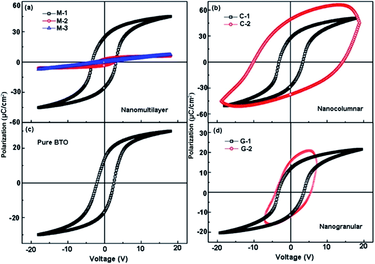 | ||
| Fig. 6 (a and b) Polarization–voltage characteristics of the BTO:NiO nanocomposite films with the nanomultilayer and nanocolumnar structure (c) P–V characteristics of the pure BTO and BTO:NiO nanogranular structure measured at room temperatures at a frequency of 1 kHz. (d) Polarization–voltage characteristics of the BTO:NiO nanocomposite films with the nanogranular structure. | ||
The nanomultilayer and nanocolumnar films can be explained within the framework of a resistance–capacitance (RC) model,10,54 arising as a result of the well-ordered 3D geometric shapes and arrangements of the BTO and NiO phases in the composite films, as shown in Fig. 7. The green part represents the BTO phase, while the pink part represents the NiO phase. The enhancement in the remanent polarization for the M-1 samples is quite considerable. In generally, for the nanomultilayer films, the effect of electrostatic interaction plays the key role in determining the values of the Pr. The electrostatic interaction is related to the properties and the thickness of non-ferroelectric layer. NiO, having a very low electrical conductivity of less than 10−13 (Ω cm)−1 at room temperature, is a Mott–Hubbard insulator dielectric.55,56 The theoretical predicted electric-field-breakdown of a Mott insulator dielectric is much larger than that of a band insulator dielectric.57,58 For the M-1 with ultra-thin NiO layers, the insulating BTO matrix ferroelectric domains will switch as the electrical field can traverse the NiO layer due to the sufficiently thin insulator layer, as shown in Fig. 7(a). For the M-2 samples with thicker NiO layer, the energy cost of the polarizing NiO increase (or even not polarized due to the pure resistance properties of NiO) and the electric field displacement in the out-of-plane direction cannot be constant throughout the BTO:NiO nanocomposites, as shown in Fig. 7(b). However, compared with the loop of BTO pure thin film, the shape of the hysteresis loop of the C-2 samples is asymmetric polarization switching behavior with a larger imprint effects, indicating a large leakage for the C-2 samples. The electronically conductive channels in the BTO:NiO nanocomposite films are the vertical interfaces of BTO and NiO, as the bulk BTO and NiO parts are more electronically insulating compared with their vertical interfaces.2 For the nanogranular structures, as shown in Fig. 6(d), the Pr value for the G-1 sample was 18 μC cm−2. This value was slightly increased compared with the pure BTO films. However, G-2 samples do not show a well-defined saturated hysteresis loop, indicating a large leakage for these samples. The polarization decreased as the formation of polydomains due to the large particles of NiO.
 | ||
| Fig. 7 Schematic diagram to show the large space charges concentration accumulated to the interface for the BTO:NiO and the movement of charges in an electric field. (a) Is the nanomultilayer with ultra-thin NiO layers and (b) is the nanomultilayer with thicker NiO layers. (c) and (d) is the nanocolumnar and nanogranular structures, respectively. The green part represents the BTO phase, while the pink part represents the NiO phase. The red and yellow circles represent the space charges. The arrows represent the ferroelectric domains. | ||
Fig. 8 shows that the leakage current (J) as a function of voltage (V) of the BTO:NiO nanocomposite films and pure BTO films at room temperature. In the present study, all the leakage current measurements have been performed with a delay time of 80 ms to avoid polarization current.59 It can be seen that the leakage current density of the nanomultilayer is the smallest among them, as shown in Fig. 8(a). The values of the leakage are of two orders of magnitude smaller than that of the pure BTO films. For the nanomultilayer structure, the J decreases with increasing the thickness of NiO layer. Fig. 8(b) shows that the values of the leakage nanocolumnar structure are comparable with the pure BTO film for the C-1. However, the leakage current density of 10−1 A cm−2 at ±100 kV cm−1 at room temperature has been observed in C-2 samples. Fig. 8(d) shows that the magnitude of leakage current density of the nanogranular thin film G-2 is approximately four orders larger than the pure films.
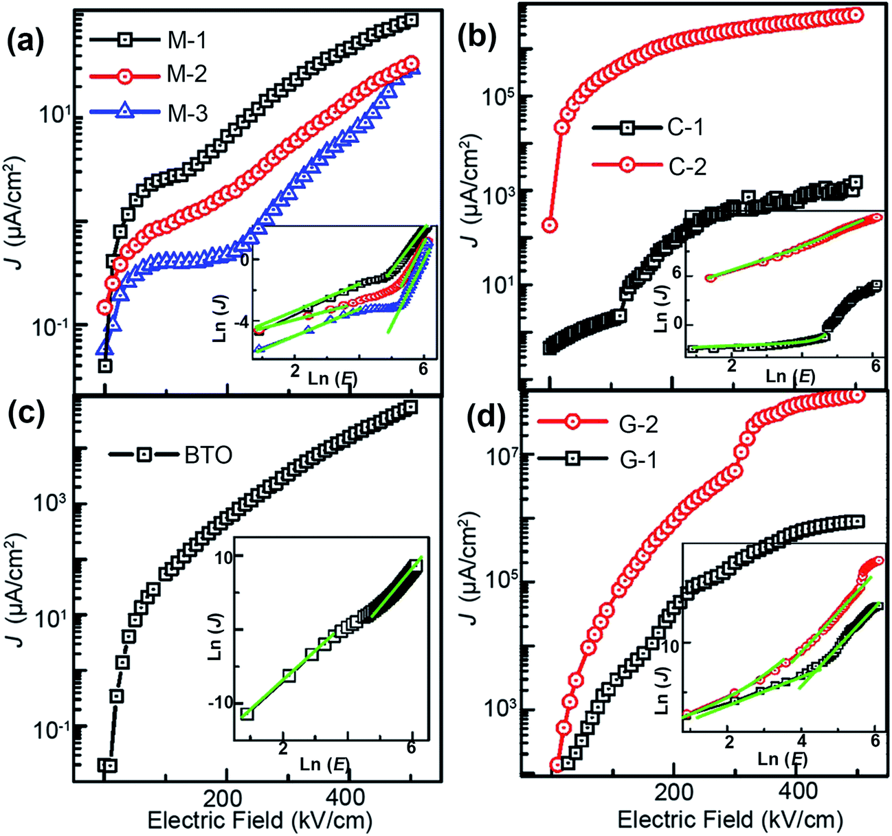 | ||
Fig. 8 (a–d) Leakage current density (J) as a function of the electric voltage (E) for the pure BTO film and BTO:NiO nanocomposite films. Inset: ln![[thin space (1/6-em)]](https://www.rsc.org/images/entities/char_2009.gif) J versus lnE for pure BTO and BTO:NiO nanocomposite films at a positive bias (the values of the slope of the fitted lines are marked). J versus lnE for pure BTO and BTO:NiO nanocomposite films at a positive bias (the values of the slope of the fitted lines are marked). | ||
After I–V data acquisition, several conductive mechanisms have been proposed for the leakage current evolutions, such as Schottky emission (SE), Poole–Frenkel emission (PF), Fowler–Nordheim tunneling (FN), and space charge limited current (SCLC).60–62 It has been well accepted that the conduction mechanisms in BTO:NiO nanocomposite films include two kinds: bulk limited (SCLC or PF) and interface limited (SE and FN). On the one hand, the J–E curves of the nanomultilayer films cannot be fitted well by the interface limited mechanism, indicating the bulk limited conduction mechanisms in these structures. Inset of Fig. 8(a) shows lnJ–lnE curves at the positive bias for the nanomultilayer. At low electric fields, the slops of curves are close to 1, meaning that the leakage current in the nanomultilayer is accorded with Ohm's law. At high electric fields, it can be fitted quite well by the SCLC mechanism and described by Child's law:63
 | (1) |
On the other hand, the J–E curves of the nanocolumnar films of C-1 and the nanogranular films can be fitted well by the modified Langmuir–Child law:67,68
| J ∝ aE + bE2 | (2) |
The dielectric properties are also strongly influenced by the presence of doping, grain boundaries, grain size, microstructure, and the concentration of charge carriers.69 Therefore, study of the dielectric properties with different microstructures may help to better understand the intrinsic and extrinsic electrical properties of BTO:NiO nanocomposite. To investigate the effect of microstructure on the electrical properties of BTO:NiO nanocomposite films, we studied the dielectric properties of BTO:NiO nanocomposite films with the NiO ratio of 10% and 20% for the nanomultilayer (M-1 and M-2), nanocolumnar (C-1 and C-2) and nanogranular (G-1 and G-2) structure. The frequency dependence of dielectric constant has been measured at room temperature. Fig. 9 shows the representative frequency dependence of the real part, ε, of relative dielectric constant of BTO:NiO. From Fig. 9, it can be seen that the BTO:NiO nanocomposite films with different microstructures have high dielectric constants compared with other BTO based nanocomposite films, such as BTO:Sm2O3, BTO:polymer and BTO:STO composite films.25,35,70–76
 | ||
| Fig. 9 ε versus tanδ for the pure BTO, NiO film and BTO:NiO nanocomposite films with different microstructures measured at 10 kHz. Some data for epitaxial ferroelectric superlattices and composite films from the literatures are also shown. | ||
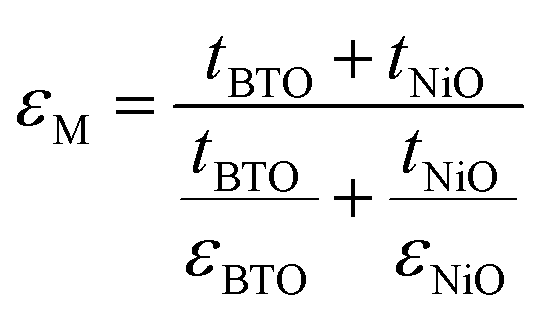
For the BTO:NiO nanomultilayer, the dielectric constant is about 646 and 873 for the M-1 and M-2 samples, respectively, much larger than the pure films. The previous work has shown that the εBTO is about 200–400 for the BTO films with thickness of 100–200 nm.77 Compared with the pure BTO and NiO films, the BTO:NiO nanomultilayers show a weak frequency dependence of the effective dielectric constant (εM) in the range from 10 kHz to 100 kHz. The lower dielectric loss in the BTO:NiO nanomultilayers at low frequency is consistent with their lower leakage current compared with the nanocolumnar and nanogranular structure, which is due to the lower concentration of the mobile charged defects restricted by the BTO:NiO interfaces. To further describe the abnormal increase of the εM for the nanomultilayers, the films can be explained within the framework of a series connection of the BTO and NiO layers,25 arising as a result of the well-ordered 3D geometric shapes and arrangements of the BTO and NiO phases in the composite films, as shown in Fig. 7(a). The εM can be expressed as:78
 | (3) |
 | ||
| Fig. 10 Frequency dependence of the dielectric constants (ε) for the pure BTO, NiO film and the BTO:NiO nanocomposite films. The green line is the calculated data for the nanomultilayer and nanogranular structure with the series model and the Maxwell–Garnett theory, respectively. | ||
For the BTO:NiO nanocolumnar films, the dielectric constant is about 1083 and 1501 at 10 kHz for C-1 and C-2 samples, respectively. Fig. 10(b) shows that C-2 films exhibit an enhancement of almost 240% in the dielectric constant compared with the pure BTO films. Though the contribution of the lateral interfaces may dominate the dielectric behavior in the nanomultilayer structures, the dielectric behavior of the BTO:NiO nanocolumnar films is totally different from those of the nanomultilayer thin films. The insulating BTO matrix exhibited ferroelectric domains, whereas the resistive NiO pillars exhibited pure dielectric properties. Compared with the nanomultilayer structure, the BTO:NiO nanocolumnar films show a strong frequency dependence of the effective dielectric constant (εC) in the range from 10 kHz to 100 kHz. On the one hand, as we discussed earlier, the not well ordered vertical nanopillar will introduce density of misfit dislocations. It is well known that dislocations have been demonstrated to be intrinsic defects and are often unavoidable in the nanocolumnar structure.18 The εC value is large for the nanocolumnar structure at low frequencies, which is likely due to the charge accumulation at the interfaces. On the other hand, the εC decreased with increasing the frequency due to the high periodic reversal of the field at the interfaces. Consequently, the contribution of charge carriers to the dielectric constant was rapidly decreased.79 However, the substantial increase in the permittivity of the BTO:NiO nanocolumnar films is very complex. On the other hand, Lee et al. found that enhanced tetragonality for the FE films gives rise to the higher permittivity.24 In this work, the BTO:NiO nanocolumnar composite films have a large average out-of-plane lattice parameter due to the vertical strain effect, which allows more room for Ti displacements and therefore enhance the dielectric properties.
As shown in Fig. 10(c), the dielectric constant is about 594 and 650 for the G-1 and G-2 samples, respectively, much larger than the pure films. For the G-2 samples, the dielectric constant is increased by 30% with respect to the pure BTO films. Interestingly, the G-1 and G-2 samples show a weak frequency dependence of the effective dielectric constant (εG) in the range from 10 kHz to 100 kHz, in line with the nanomultilayer structures. Compared with the nanomultilayer and nanocolumnar structures, the lower dielectric constant in the nanogranular structure at low frequency is consistent with their higher leakage current, as shown in Fig. 8(d). The dielectric property of nanogranular composite films has been studied by previous researchers.80,81 The insulating BTO matrix exhibited ferroelectric domains, whereas the resistive NiO nanoparticles (NPs) exhibited pure dielectric properties. It is noted that, the dielectric property could be effectively modified in the nanogranular structure by a proper addition of NiO nanoparticles, satisfying with the Maxwell–Garnett theory as follows:82
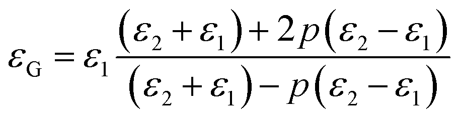 | (4) |
Conclusions
In this study, epitaxial BTO:NiO nanocomposite films with different NiO fractions and microstructures have been grown on (001) Nb:STO substrates by PLD. For the composite films with a NiO ratio of 10% and 20%, the microstructures such as nanomultilayer, nanocolumnar and nanogranular have been successfully tuned by controlling the growth modes of the BTO and NiO. The values of polarization and dielectricity are sensitive to the microstructure. By tuning the microstructures, significantly enhanced polarization (24 μC cm−2 for the nanomultilayer structures) and dielectric constant (873 and 1320 for the nanomultilayer and nanocolumnar structures, respectively) could be realized in these composite films. Our results show that the FE properties of BTO based nanocomposite films can be more effectively modulated by tuning their microstructures.Acknowledgements
This work is supported by the National Natural Science Foundation of China (Grant No. 11604073 and 51372064), the Nature Science Foundation of Hebei Province (Grant No. A2017201104, E2017201227), the Natural Science Foundation of Educational Department of Hebei Province (BJ2017046), the One Province and One School fund and the Graduate Student Innovation fund Project in Hebei Province (No. CXZZBS2017023).Notes and references
- M. Fan, B. Zhang, H. Wang, J. Jian, X. Sun, J. J. Huang, L. G. Li, X. H. Zhang and H. Y. Wang, Adv. Mater., 2017, 29, 1606861 CrossRef PubMed.
- S. Cho, C. Yun, S. Tappertzhofen, A. Kursumovic, S. Lee, P. Lu, Q. X. Jia, M. Fan, J. Jian, H. Y. Wang, S. Hofmann and J. L. MacManus-Driscoll, Nat. Commun., 2016, 7, 12373 CrossRef CAS PubMed.
- O. M. Hemeda, K. R. Mahmoud, T. Sharshar, M. Elsheshtawy and M. A. Hamad, J. Magn. Magn. Mater., 2017, 429, 124–128 CrossRef CAS.
- M. Zhuravlev, R. Sabirianov, S. Jaswal and E. Tsymbal, Phys. Rev. Lett., 2005, 94, 246802 CrossRef.
- X. Q. Liu, J. Iocozzia, Y. Wang, X. Cui, Y. H. Chen, S. Q. Zhao, Z. Li and Z. Q. Lin, Energy Environ. Sci., 2017, 10, 402–434 CAS.
- W. J. Ong, L. L. Tan, S. P. Chai, S. T. Yong and A. R. Mohamed, ChemSusChem, 2014, 7, 690–719 CrossRef CAS PubMed.
- X. K. Ning, Z. J. Wang and Z. D. Zhang, Adv. Mater. Interfaces, 2015, 2, 1500302 CrossRef.
- A. Chen, J.-M. Hu, P. Lu, T. N. Yang, W. R. Zhang, L. G. Li, T. Ahmed, E. Enriquez, M. Weigand, Q. Su, H. Y. Wang, J.-X. Zhu, J. L. MacManus-Driscoll, L.-Q. Chen, D. Yarotski and Q. X. Jia, Sci. Adv., 2016, 2, e1600245 Search PubMed.
- H. M. Zheng, Q. Zhan, F. Zavaliche, M. Sherburne, F. Straub, M. P. Cruz, L. Q. Chen, U. Dahmen and R. Ramesh, Nano Lett., 2006, 6, 1401–1407 CrossRef CAS PubMed.
- X. K. Ning, Z. J. Wang and Z. D. Zhang, Adv. Funct. Mater., 2014, 24, 5393–5401 CrossRef CAS.
- M. Zhou, Y. L. Li, I. Jeon, Q. H. Yi, X. B. Zhu, X. W. Tang, H. Y. Wang, L. Fei, Y. P. Sun, S. G. Deng, Y. Matsuo, H. M. Luo and G. F. Zouc, Sci. Rep., 2016, 6, 26390 CrossRef CAS PubMed.
- S. Fusil, V. Garcia, A. Barthélémy and M. Bibes, Annu. Rev. Mater. Res., 2014, 44, 91 CrossRef CAS.
- T. Walther, R. Köferstein and S. G. Ebbinghaus, J. Am. Ceram. Soc., 2017, 100, 1502–1507 CrossRef CAS.
- H. L. Wang, X. K. Ning and Z. J. Wang, RSC Adv., 2015, 5, 76783–76787 RSC.
- X. K. Ning, Microstructure of the Nanostructured Oxide Composite Thin Films and Its Functional Properties, Outlook and Challenges of Nano Devices, Sensors, and MEMS, Springer International Publishing, 2017, pp. 397–427 Search PubMed.
- P. Zubko, N. Jecklin, A. Torres-Pardo, P. Aguado-Puente, A. Gloter, C. Lichtensteiger, J. Junquera, O. Steìphan and J.-M. Triscone, Nano Lett., 2012, 12, 2846–2851 CrossRef CAS PubMed.
- M. Dawber, N. Stucki, C. Lichtensteiger, S. Gariglio, P. Ghosez and J. Triscone, Adv. Mater., 2007, 19, 4153–4159 CrossRef CAS.
- W. W. Li, W. Zhang, L. Wang, J. X. Gu, A. P. Chen, R. Zhao, Y. Liang, H. Z. Guo, R. J. Tang, C. C. Wang, K. J. Jin, H. Y. Wang and H. Yang, Sci. Rep., 2015, 5, 11335 CrossRef PubMed.
- H. Huang, Nat. Photonics, 2010, 4, 134–135 CrossRef CAS.
- V. Garcia, S. Fusil, K. Bouzehouane, S. Enouz-Vedrenne, N. D. Mathur, A. Barthélémy and M. Bibes, Nature, 2009, 460, 81 CrossRef CAS PubMed.
- M. Dawber and E. Bousquet, MRS Bull., 2013, 38, 1048–1055 CrossRef CAS.
- E. Bousquet, M. Dawber, N. Stucki, C. Lichtensteiger, P. Hermet, S. Gariglio, J.-M. Triscone and P. Ghosez, Nature, 2008, 452, 732–736 CrossRef CAS PubMed.
- H. Tabata, H. Tanaka and T. Kawai, Appl. Phys. Lett., 1994, 65, 1970–1972 CrossRef CAS.
- H. N. Lee, H. M. Christen, M. F. Chisholm, C. M. Rouleau and D. H. Lowndes, Nature, 2005, 433, 395–399 CrossRef CAS PubMed.
- B. He and Z. J. Wang, ACS Appl. Mater. Interfaces, 2016, 8, 6736–6742 CAS.
- J. J. Peng, C. Song, B. Cui, F. Li, H. J. Mao, G. Y. Wang and F. Pan, Appl. Phys. Lett., 2015, 107, 182904 CrossRef.
- Y. Liu, Y. L. Zhu, Y. L. Tang, Y. J. Wang, Y. X. Jiang, Y. B. Xu, B. Zhang and X. L. Ma, Nano Lett., 2017, 17, 3619 CrossRef CAS PubMed.
- F. F. Ge, L. Bai, W. D. Wu, L. H. Cao, X. M. Wang, Y. J. Ma, S. J. Han, H. P. Wang, X. Y. An, H. B. Wang and J. Shen, J. Cryst. Growth, 2015, 312, 2489–2493 CrossRef.
- F. F. Ge, X. M. Wang, L. H. Cao, J. Li, H. L. Zhang, H. P. Wang, Y. Bai, H. B. Wang, J. Shen and W. D. Wu, Nanoscale Res. Lett., 2010, 5, 834–838 CrossRef CAS PubMed.
- Z. R. Wang, T. Hu, L. W. Tang, M. Ning, C. L. Song, G. R. Han, W. J. Weng and P. Y. Du, Appl. Phys. Lett., 2008, 93, 222901–222904 CrossRef.
- W. D. Wu, Y. J. He, F. Wang, Z. H. Chen, Y. J. Tang and W. G. Sun, J. Cryst. Growth, 2006, 289, 408–413 CrossRef CAS.
- Y. J. Wu, H. L. Wang, X. K. Ning, Z. J. Wang and Q. Wang, J. Inorg. Mater., 2015, 30, 207–213 CrossRef CAS.
- A. Cazacu, L. Curecheriu, A. Neagu, L. Padurariu, A. Cernescu, I. Lisiecki and L. Mitoseriu, Appl. Phys. Lett., 2013, 102, 222903 CrossRef.
- H. Zheng, J. Wang, S. E. Lofland, Z. Ma, L. Mohaddes-Ardabili, T. Zhao, L. Salamanca-Riba, S. R. Shinde, S. B. Ogale, F. Bai, D. Viehland, Y. Jia, D. G. Schlom, M. Wuttig, A. Roytburd and R. Ramesh, Science, 2004, 303, 661 CrossRef CAS PubMed.
- O. J. Lee, S. A. Harrington, A. Kursumovic, E. Defay, H. Y. Wang, Z. X. Bi, C.-F. Tsai, L. Yan, Q. X. Jia and J. L. MacManus-Driscoll, Nano Lett., 2012, 12, 4311–4317 CrossRef CAS PubMed.
- R. Zhao, W. W. Li, J. H. Lee, E. M. Choi, Y. Liang, W. Zhang, R. J. Tang, H. Y. Wang, Q. X. Jia, J. L. MacManus-Driscoll and H. Yang, Adv. Funct. Mater., 2014, 24, 5240–5245 CrossRef CAS.
- P. Lunkenheimer, A. Loidl, C. R. Ottermann and K. Bange, Phys. Rev. B: Condens. Matter Mater. Phys., 1991, 44, 5927 CrossRef CAS.
- J. B. Wu, C. W. Nan, Y. H. Lin and Y. Deng, Phys. Rev. Lett., 2002, 89, 271601 CrossRef PubMed.
- C. Pecharromán, F. Esteban-Betegón, J. F. Bartolomé, S. López-Esteban and J. S. Moya, Adv. Mater., 2001, 13, 1541–1544 CrossRef.
- M. Saleem, I. S. Kim, J. S. Song, S. J. Jeong, M. S. Kim and S. Yoon, Ceram. Int., 2014, 40, 7329–7335 CrossRef CAS.
- S. J. Callori, J. Gabel, D. Su, J. Sinsheimer, M. V. Fernandez-Serra and M. Dawber, Phys. Rev. Lett., 2012, 109, 067160 CrossRef PubMed.
- L. X. Li, R. X. Fu, Q. W. Liao and L. J. Ji, Ceram. Int., 2012, 38, 1915 CrossRef CAS.
- J. Q. Huang, P. Y. Du, W. J. Weng and G. R. Han, J. Electroceram., 2008, 21, 394 CrossRef CAS.
- S. Li, X. H. Wei, Y. Lei, X. C. Yuan and H. Z. Zeng, Appl. Surf. Sci., 2016, 389, 977 CrossRef CAS.
- D. Nuzhnyy, J. Petzelt, V. Bovtun, T. Ostapchuk, M. Savinov, M. Kempa, P. Bednyakov, L. Fernández-Garciá, T. Rodriguez-Suarez and J. L. Menendéz, Ferroelectrics, 2016, 500, 1 CrossRef CAS.
- F. C. Frank and J. H. van der Merwe, Proc. R. Soc. London, Ser. A, 1949, 198, 205 CrossRef CAS.
- S. L. Yuan, Y. P. Yang, Z. C. Xia, G. Peng, G. H. Zhang, J. Tang, J. Liu, L. J. Zhang, Q. H. Zhong, S. Liu, L. Chen, W. Feng, Z. Y. Li, L. Liu, G. Q. Zhang, F. Tu and C. S. Xiong, Solid State Commun., 2002, 123, 55 CrossRef CAS.
- D. B. Williams and C. B. Carter, Transmission Electron Microscopy: A Textbook for Materials Science, Plenum, New York, 1996 Search PubMed.
- B. S. Guiton, H. Wu and P. K. Davies, Chem. Mater., 2009, 20, 2860 CrossRef.
- Y. Ni, W. F. Rao and A. G. Khachaturyan, Nano Lett., 2009, 9, 3275 CrossRef CAS PubMed.
- N. Ortega, A. Kumar, O. A. Maslova, Y. I. Yuzyuk, J. F. Scott and R. S. Katiyar, Phys. Rev. B: Condens. Matter Mater. Phys., 2011, 83, 144108 CrossRef.
- K. Boldyreva, L. Pintilie, A. Lotnyk, I. B. Misirlioglu, M. Alexe and D. Hesse, Appl. Phys. Lett., 2007, 91, 122915 CrossRef.
- K. J. Choi, M. Biegalski, Y. L. Li, A. Sharan, J. Schubert, R. Uecker, P. Reiche, Y. B. Chen, X. Q. Pan, V. Gopalan, L.-Q. Chen, D. G. Schlom and C. B. Eom, Science, 2004, 306, 1005–1009 CrossRef CAS PubMed.
- S. A. Fedoseev, A. V. Pan, S. Rubanov, I. A. Golovchanskiy and O. V. Shcherbakova, ACS Nano, 2013, 7, 286 CrossRef CAS PubMed.
- K. Terakura, A. R. Williams, T. Oguchi and J. Kubler, Phys. Rev. Lett., 1984, 52, 1830 CrossRef CAS.
- J. M. Mckay and V. E. Henrich, Phys. Rev. Lett., 1984, 53, 2343 CrossRef CAS.
- D. Puggioni, G. Giovannetti, M. Capone and J. M. Rondinelli, Phys. Rev. Lett., 2015, 115, 087202 CrossRef PubMed.
- H. Gomi, T. J. Inagaki and A. Takahashi, Phys. Rev. B, 2016, 93, 035105 CrossRef.
- C. Bhardwaj and D. Kaur, J. Alloys Compd., 2014, 595, 158 CrossRef CAS.
- I. Boerasu, L. Pintilie, M. Pereira, M. I. Vasilevskiy and M. J. M. Gomes, J. Appl. Phys., 2003, 93, 4776 CrossRef CAS.
- M. T. Chentir, E. Bouyssou, L. Ventura and C. Anceau, J. Appl. Phys., 2009, 105, 061605 CrossRef.
- D. Lee, S. H. Baek, T. H. Kim, J.-G. Yoon, C. M. Folkman, C. B. Eom and T. W. Noh, Phys. Rev. B: Condens. Matter Mater. Phys., 2011, 84, 125305 CrossRef.
- W. Li, R. Zhao, R. Tang, A. Chen, W. Zhang, X. Lu, H. Wang and H. Yang, ACS Appl. Mater. Interfaces, 2014, 6, 5356–5361 CAS.
- R. Barman and D. Kaur, J. Alloys Compd., 2015, 644, 506–512 CrossRef CAS.
- N. Mott, J. Solid State Chem., 1990, 88, 5 CrossRef CAS.
- M. Imada, A. Fujimori and Y. Tokura, Rev. Mod. Phys., 1998, 70, 1039 CrossRef CAS.
- X. Qi, J. Dho, R. Tomov, M. G. Blamire and J. L. MacManus- Driscoll, Appl. Phys. Lett., 2005, 86, 062903 CrossRef.
- Z. Wen, X. Shen, J. X. Wu, D. Wu, A. D. Li, B. Yang, Z. Wang, H. Z. Chen and J. L. Wang, Appl. Phys. Lett., 2010, 96, 202904 CrossRef.
- N. H. Vasoya, V. K. Lakhani, P. U. Sharma, K. B. Modi, R. Kumar and H. H. Joshi, J. Phys.: Condens. Matter, 2006, 18, 8063–8092 CrossRef CAS.
- H.-N. Tsai, Y.-C. Liang and H.-Y. Lee, J. Cryst. Growth, 2005, 284, 65–72 CrossRef CAS.
- M. Bousquet, L. Batista, J. L. Dellis, A. Boulle, U. Rabe, O. Durand-Drouhin, Y. Gagou, L. Dupont, V. Viallet, A. Zeinert, S. Hirsekorn and N. Lemée, J. Appl. Phys., 2014, 116, 194104 CrossRef.
- S. A. Harrington, J. Y. Zhai, S. Denev, V. Gopalan, H. Y. Wang, Z. X. Bi, S. A. T. Redfern, S. H. Baek, C. W. Bark, C. B. Eom, Q. X. Jia, M. E. Vickers and J. L. MacManus-Driscoll, Nat. Nanotechnol., 2011, 6, 491–495 CrossRef CAS PubMed.
- F. Khatkhatay, A. Chen, J. H. Lee, W. Zhang, H. Abdel-Raziq and H. Wang, ACS Appl. Mater. Interfaces, 2013, 5, 12541–12547 CAS.
- N. Suzuki, M. B. Zakaria, N. L. Torad, K. C.-W. Wu, Y. Nemoto, M. Imura, M. Osada and Y. Yamauchi, Chem.–Eur. J., 2013, 19, 4446–4450 CrossRef CAS PubMed.
- R. Popielarz, C. K. Chiang, R. Nozaki and J. Obrzut, Macromolecules, 2001, 34, 5910–5915 CrossRef CAS.
- S. F. Wang, Y. R. Wang, K. C. Cheng and Y. P. Hsaio, Ceram. Int., 2009, 35, 265–268 CrossRef CAS.
- B. H. Hoerman, G. M. Ford, L. D. Kaufmann and B. W. Wessels, Appl. Phys. Lett., 1998, 73, 2248 CrossRef CAS.
- A. K. Tagantsev, V. O. Sherman, K. F. Astafiev, J. Venkatesh and N. Setter, J. Electroceram., 2003, 11, 5–66 CrossRef CAS.
- L. J. Chen, L. P. Li and G. S. Li, J. Solid State Chem., 2008, 181, 2073–2077 CrossRef CAS.
- Z. Wang, T. Hu, L. Tang, N. Ma, C. Song, G. Han, W. Weng and P. Du, Appl. Phys. Lett., 2008, 93, 222901 CrossRef.
- N. Tsutsumi, R. Kosugi, K. Kinashi and W. Sakai, ACS Appl. Mater. Interfaces, 2016, 8, 16816–16822 CAS.
- T. Liu, Y. Pang, M. Zhu and S. Kobayashi, Nanoscale, 2014, 6, 2447–2454 RSC.
Footnote |
| † Electronic supplementary information (ESI) available. See DOI: 10.1039/c7ra06627a |
| This journal is © The Royal Society of Chemistry 2017 |