
 Open Access Article
 This Open Access Article is licensed under a
 Creative Commons Attribution 3.0 Unported Licence
Growth of single-crystalline cubic structured tin(II) sulfide (SnS) nanowires by chemical vapor deposition†
Devika Mudusu‡
ab,
Koteeswara Reddy Nandanapalli‡ *ac,
Sreekantha Reddy Dugasani‡c,
Jang Won Kangad,
Sung Ha Park*c and
Charles W. Tu*ae
*ac,
Sreekantha Reddy Dugasani‡c,
Jang Won Kangad,
Sung Ha Park*c and
Charles W. Tu*ae
aDepartment of Nanobio Materials and Electronics, Gwangju Institute of Science and Technology, Gwangju-500712, Republic of Korea. E-mail: dr_nkreddy@rediffmail.com; ctu@ucsd.edu
bSchool of Advanced Materials Science & Engineering, Sungkyunkwan University, Suwon, Gyeonggi-do 440746, South Korea
cDepartment of Physics, Sungkyunkwan University, Suwon 440746, South Korea. E-mail: sunghapark@skku.edu
dDepartment of Emerging Materials Science, Daegu Gyeongbuk Institute of Science and Technology (DGIST), Daegu 42988, South Korea
eDepartment of Electrical and Computer Engineering, University of California, San Diego, La Jolla, CA 92093-0407, USA
First published on 25th August 2017
Abstract
Single crystalline tin(II) sulfide (SnS) nanowires are synthesized using a chemical vapor deposition (CVD) method with the support of gold as catalyst. Field emission electron microscopy studies show that SnS nanostructures grown at temperatures between 600 and 700 °C have wire-like morphology. These nanowires have an average diameter between 12 and 15 nm with lengths up to several microns. These NWs consist of uniform and smooth surfaces, and exhibit nearly stoichiometric chemical composition (Sn/S = 1.13). Transmission electron microscopy analysis reveals that the NWs consist of single crystalline cubic crystal structure with a preferential growth direction of 〈100〉. Field-effect transistor devices fabricated with SnS nanowires show that the nanowires consist of p-type conductivity along with carrier density of 6 × 1018 cm−3.
Introduction
One-dimensional (1D) nanostructures of semiconductor materials have received great attention in the development of various prototype devices due to their distinct properties.1–6 As compared to their bulk counterparts, semiconductor nanostructures exhibit high surface-to-volume ratio, and unique electrical and optical properties. In this regard, tin(II) sulfide (SnS), IV–VI group compound semiconductor, has received considerable attention due to its favorable chemical and physical properties. In general, SnS exhibits a direct optical band gap of 1.35 eV and p-type electrical conductivity. It is a double-layer structured compound, and usually crystallizes in the form of orthorhombic structure with lattice parameters a = 0.433, b = 1.119, and c = 0.398 nm. The electrical and optical properties of SnS can be easily tailored by doping with appropriate dopants.7–10 It exhibits stable structural and optical properties, even at low temperatures.11 Further, the constituent elements of SnS are abundant in nature, and do not pose any health or environmental hazards. Based on the optical band gap, the possible light conversion efficiency of SnS-based devices is about 25%.12 These interesting properties make SnS a suitable candidate for the development of various electrical and optoelectronic devices.13Over the past couple of years, the synthesis of nanostructures with specific morphologies and crystal structures has been of great concern, since the optical and electrical properties of materials strongly depend on their shape and size, as well as structure.14 Thus, the ability to tune the physical properties of SnS at nanoscale probably leads its applications to diverging fields. In this regard, different types of SnS nanostructures, including nanoflakes, nanowires,15 nanorods,16–20 nanobelts,21 nanoflowers,22 nanoparticles,23–25 nanoboxes,26,27 and nanosheets28,29 have been realized, using various synthetic methods. Noticeably, most of the realized SnS nanostructures consist of orthorhombic crystal structure. However, Greyson et al. have synthesized zinc blende (a = b = c = 0.585 nm) structured SnS nano- and micro-crystals using thermal decomposition of tine chloride and sulfur powder.30 Further, as compared to usual orthorhombic SnS nanostructures, these zinc blende structured SnS nanocrystals exhibit quite different optical properties.
On the other hand, at higher temperatures, SnS exhibits a phase transition from orthorhombic to tetragonal, and its lattice parameters a and c equal 0.423, and b = 1.151 nm, respectively. In our recent investigations on the development of nanocrystalline SnS structures by a thermal evaporation technique, we noticed that SnS also exhibits a transition from orthorhombic to tetragonal phase at a growth temperature of 410 °C, which is treated as a phase transition temperature.31 At this temperature, the lattice parameters of tetragonal SnS are evaluated (a = c) as 0.42 and b = 1.13 nm, respectively, and its Sn to S atomic percent ratio is found to be ∼1.2.
In this direction, by keeping all these issues in mind, we have initiated the synthesis of SnS nanowires by chemical vapor deposition (CVD) using gold (Au) as metal catalyst under the well-established vapor–liquid–solid (VLS) process, and have explored their physical and chemical properties. The SnS nanostructures grown under optimized conditions are highly dense, long, and have uniform surface morphology and excellent chemical stoichiometry. In this paper, we report the methodology for the growth of SnS nanostructures on two different substrates, and the optimized growth conditions for uniform single crystalline SnS nanowires. Furthermore, a plausible growth mechanism is also reported and discussed.
Experimental procedure
Materials and chemicals
(100) n-type silicon (Si, ρ = 0.005 Ω cm) substrate, (001) sapphire substrate (c-plane). Sulfur-rich SnS powder (Sn/S atomic% ratio of 0.95) synthesized by following the procedure reported elsewhere32 and gold (99.99) was purchased from Sigma-Aldrich.Growth of SnS nanostructures
SnS nanostructures were synthesized in a homebuilt chemical vapor deposition (CVD) system. Fig. SI1 in the ESI† shows a schematic of the procedure. A fine power of SnS was taken in a ceramic boat, and placed 5 cm away from the center of the tube. Cleaned (100) n-type Si and (001) sapphire substrates coated with gold (5 nm) (see SI2†) were placed at the center of the tube under downstream direction of the carrier gas. Then, the CVD system was initially evacuated to base pressure of 4 × 10⁻² Torr, and then purged with argon gas with the flow rate of 100 sccm (standard cubic centimeter per minute) for three times. The system was then heated to a fixed temperature. In the present work, the growth was carried out at different temperatures varying from 500 to 950 °C. The growth time and operating pressure of the system were kept constant at 10 min and 20 Torr, respectively. After successful completion of the process, the system was allowed cool-down to room temperature.Fabrication of FET devices
Field-effect transistor devices were fabricated on Si/SiO2 substrates (2 × 2 cm2) by photolithography. Here, highly doped p-type Si substrates (ρ = 5 × 10⁻³ Ω cm) with thermally grown 100 nm thick SiO2 layer were used as gate electrodes. Initially, SnS nanowires were detached from substrates by sonication into ethanol solvent, and they were dispersed on Si/SiO2 substrates. Photoresists were deposited by spin-coating, and dried on hot-plate at pre-optimized temperatures. Patterns were developed by exposing the samples to light under mask, and followed by a lift-off process. Bilayer contacts (Ti/Au) were deposited by e-beam evaporation with a thickness of ∼100/50 nm, and then the lift-off process was carried out.Characterization
Field emission scanning electron microscopy (FESEM) was used to examine the surface morphology. Energy dispersive X-ray spectroscopy (EDS) embedded with FESEM was adopted to estimate the chemical composition of the as-synthesized structures. High resolution FESEM images have been analyzed by ImageJ 1.43u (Wayne Rasband, National Institutes of Health, USA; http://rsb.info.nih.gov/ij). Transmission electron microscopy (TEM), high-resolution TEM (HRTEM) and selected area electron diffraction (SAED) were used to confirm the crystallographic properties. Finally, the electrical characteristics of SnS nanowires were investigated by studying the FET devices using probe station (with four-probe configuration) attached with semiconductor parameter analyzer.Results and discussion
The product grown on both substrates at all temperatures appears silver gray in color, which is very similar to the color of SnS source powder. FESEM images of SnS nanostructures grown at 500 °C (Fig. SI3(a) and (b)†) consist of button-mushroom like crystals (some of them have spherical shaped bright particles as heads). After increase of the growth temperature from 500 to 550 °C, the button-mushroom shaped crystals are slightly elongated, and look like NWs (Fig. SI3(c) and (d)†). These nanowires consist of gold particle as head. The average length of the nanowires grown on both the substrates is about 200 nm; however, the diameter of nanowires grown on Si substrate is slightly different than that of the nanowires on sapphire substrate. Noticeably, the diameter of the nanowires on both the substrates is clearly lower than the diameter of gold particles, as can be clearly seen from the insets of (Fig. SI3(c) and (d)†). For example, the average diameter of SnS nanowires grown at 550 °C is about 17 (19 in case of Si) nm, and their corresponding Au nanoparticles average diameter is 22 nm.FESEM images of SnS nanowires grown at 600 °C (Fig. SI3(e) and (f)†) reveal that the structures grown at 600 °C consist of different morphologies, including nanowires, nanorods, helices, and aggregated balls with different dimensions (shown in Fig. SI4(a)†). As compared to the structures grown at 550 °C, these structures consist of a greater number of NWs, which have the length of 2–4 times that of a micron (see SI4(b)†). FESEM images of SnS nanostructures grown on sapphire and Si substrates at 650 °C are shown in Fig. 1. It reveals that the as-grown structures consist of lengthy nanowires, which have uniform and smooth surface morphology. The growth of nanostructures on both the substrates is freestanding and denser. Note that these nanowires consist of high aspect ratio, since the average diameter of the nanowires vary between 13 and 14 nm, which depends on nature of Au crystallites size over substrates (as can be seen from the insets of Fig. 1(a) and (b)), and their lengths are up to several microns (see SI5†). Yue et al. have realized similar SnS nanostructures at 800 °C growth temperature using SnS + S powders as precursors by gold nanoparticles assisted chemical vapor deposition on ITO substrates under the flow of Ar + H2 gases.15 Similar to present work, Ga2S3 nanowires have been realized in ambient pressure CVD system by using Ga metal and H2S (∼400 sccm) as sources of Ga and S at growth temperatures of 650–800 °C.33 On the other hand, Wu et al. developed led sulfide nanowires on several metal thin films coated substrates using PbCl2 and S as precursors for Pb and S at growth temperatures varied between 600 and 650 °C.34
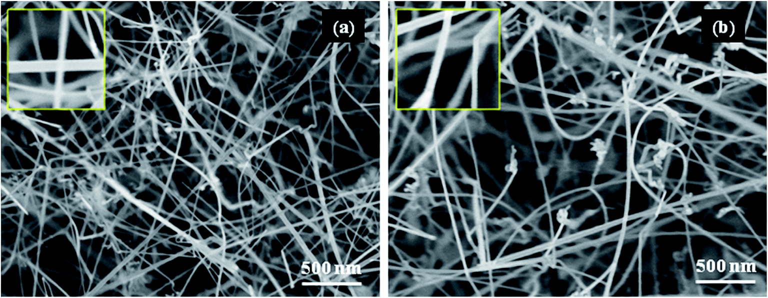 | ||
| Fig. 1 FESEM images of SnS nanostructures grown at the growth temperature of 650 °C on (a) sapphire and (b) Si substrates, respectively. | ||
With further increase of growth temperature from 650 to 950 °C, the morphology of SnS nanostructures becomes trivial, and their growth on both the substrates gradually reduced. It can be seen in Fig. SI6,† which presents FESEM images of SnS nanostructures grown at 700, 800, and 950 °C. On the other hand, the structures grown at above 700 °C showed tapering on the surface of nanowires, which could be due to uncatalyzed growth of SnS over the sidewalls of nanowires. In this region, the length of nanowires also gradually decreases with the increase of growth temperature, whereas their diameters increase. To explore the impact of growth temperature on the diameter of SnS nanowires, the nanowires' diameters were extracted by analyzing FESEM images (recorded at 60k magnification) with ImageJ software.35,36
Variation of average diameter (AD, see SI7†) of SnS nanowires, grown on sapphire (SA) and silicon (Si) substrates, as function of growth temperature (GT) along with its demonstrative FESEM images is shown in Fig. 2. It clearly reveals that at all growth temperatures, the nanowires grown on Si substrates have slightly larger diameters than that of nanowires on SA substrates, which is probably attributed to the size of Au grains (or crystals) on different substrates (see SI2†).37 The nanowires grown at the growth temperature of 550 °C consist of an average diameter of 17 nm (19 nm in case of Si). With the increase of growth temperature from 550 to 650 °C, AD of nanowires gradually decreases and reaches a low value of 13 (14) nm at 650 °C, which is highlighted with a green line in Fig. 2a. Above this temperature, AD increases exponentially with increasing growth temperature. As discussed in the literature about the growth of nanostructures by CVD technique, the variation in diameter of nanowires strongly attributed to growth kinetics of nanostructures.38 It reveals that the growth rate along the axial direction of SnS could be high at around 650 °C due to lower nucleation barrier on the top facet of nanowires than the vertical sidewalls. This greatly lengthens the nanowires much faster along their axial direction.39 However, above this temperature, the increase in diameter of nanowires attributed to the competing growth on the sidewalls (radial) of nanowires through uncatalyzed deposition.37 Similar changes in the diameter of InAs nanowires, grown by metal–organic CVD system, have been observed by Li et al.40
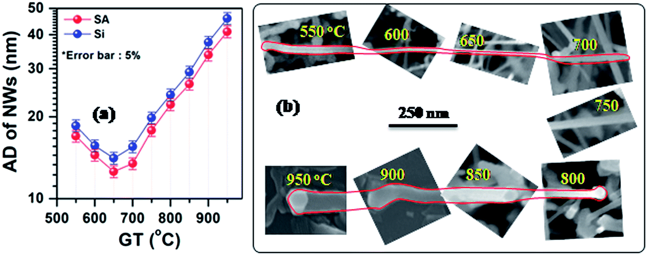 | ||
| Fig. 2 (a) Variation of average diameter (AD) of SnS nanowires, grown on sapphire (SA) and silicon (Si) substrates, as a function of growth temperature (GT) (hint: error bar represents error in percent of data) and (b) its pictorial representation by selected portion of FESEM images of SnS nanowires grown on Si substrates. | ||
The SnS structures grown on Si substrates at a growth temperature of 650 °C consist of smooth, long, and denser nanowires, and have an average diameter of 14 nm. These unique nanostructures, therefore, have been chosen for further studies.
Chemical composition analysis by EDS (see SI8†) reveals that the as-grown SnS nanowires consist of ∼53 atomic% of Sn and 47 atomic% of S, and the Sn/S atomic% ratio is found to be 1.13. This indicates that the as-grown SnS nanowires have nearly stoichiometric chemical composition between the constituents. XRD profile of SnS nanowires grown at 650 °C is shown in Fig. 3(a). This indicates that SnS nanowires consist of a predominant peak at 32.86° along with a several minor peaks diffracted at different angles. All the diffraction peaks are indexed to cubic and orthorhombic structured SnS (PDF # 892755 and 831758). It implies that the as-grown SnS nanowires at 650 °C not contain any other Sn–S phases like SnS2 and Sn2S3. As presented in Fig. 3(a), first, second, fourth, and seventh peaks belong to orthorhombic SnS, whereas the dominant peak along with third peak belongs to cubic structured SnS. Presence of a sharp and narrow (200) peak clearly indicates that the as-grown nanowires are highly crystalline in quality and grown along (100) planes of cubic structured SnS. Presence of minor diffraction peaks of orthorhombic SnS probably arose either from orthorhombic structured SnS thin film or nanowires, which could be developed along with cubic structured SnS nanowires. Nearly similar to our results, Seo et al. have observed cubic as well as hexagonal crystal structures in zinc selenide (ZnSe) nanowires grown by chemical vapor deposition on gold nanoparticles dispersed ITO substrates.41
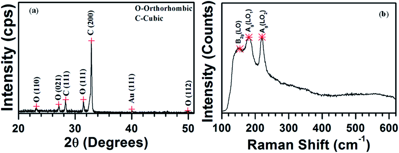 | ||
| Fig. 3 (a) XRD pattern and (b) Raman spectrum of SnS nanowires grown on Si substrate at the growth temperature of 650 °C. | ||
The Raman spectrum of SnS nanowires grown at 650 °C, shown in Fig. 3(b), exhibits three distinguishable peaks, which are assigned to three different single-phonon oriented longitudinal optical (LO) vibrational modes, i.e. B2g(LO), Ag(LO1) and Ag(LO2).42 As compared to the Raman spectra of SnS thin films31,42 or orthorhombic nanostructures,15,43,44 the cubic structured SnS nanowires peculiarly consist of Ag(LO2) peak as sharp and dominant, which is probably attributed the preferential growth of structures. This clearly reveals that the as-grown SnS nanowires consist of pure single phase.
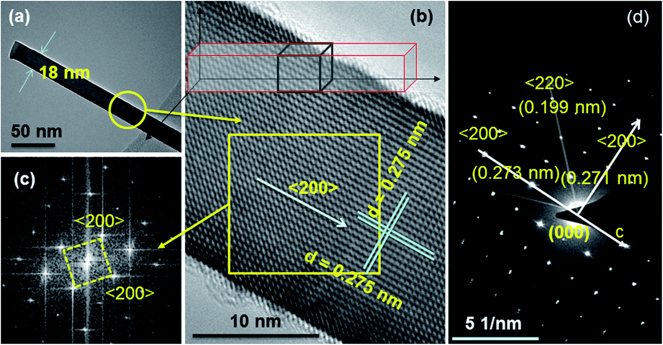
Fig. 4 shows TEM, HRTEM, and SAED images of SnS nanowires grown on Si substrate at 650 °C. Fig. 4(a) reveals that the as-grown SnS nanowires consist of low diameter of about 18 nm, and are uniform along their length. The results are consistent with the FESEM data. Fig. 4(b) shows HRTEM image of SnS nanowire. The lattice fringes of SnS nanowire in all the directions are very clear and periodic, which indicate the as-grown SnS nanowires are single crystalline crystallites, and have very good crystalline quality. The estimated d-spacing values from two-dimensional fast Fourier transformation (FFT) analysis on HRTEM image (Fig. 4(c)) is ∼0.275 nm, which corresponds to the (200) planes of cubic SnS (face-centered cubic, space group: F![[4 with combining macron]](https://www.rsc.org/images/entities/char_0034_0304.gif) 3m, PDF #892755). This reveals that the growth direction of SnS nanowires is parallel to the axis of the (100) planes. The cell parameter(s), calculated using the standard equation for cubic lattices (see SI9†), is found to be a = b = c = 0.55 nm, which exactly matches the standard cubic structured SnS data (PDF #892755).
3m, PDF #892755). This reveals that the growth direction of SnS nanowires is parallel to the axis of the (100) planes. The cell parameter(s), calculated using the standard equation for cubic lattices (see SI9†), is found to be a = b = c = 0.55 nm, which exactly matches the standard cubic structured SnS data (PDF #892755).
 | ||
| Fig. 4 (a) TEM, (b) HRTEM (inset shows the schematic representation of SnS nanowires growth), (c) FFT taken on HRTEM, and (d) SAED images of SnS nanowires grown on Si substrate at the growth temperature of 650 °C. | ||
Fig. 4(d) shows SAED image recorded on SnS nanowires at lower magnification TEM object, and the diffraction spots can be indexed to the face-centered cubic (fcc)-type SnS with a lattice constant of 0.55 nm. The presence of regular diffraction spots clearly confirms that the as-grown SnS nanowires are single crystalline cubic crystals, and have growth direction along the (100) planes. The possible reason(s) for the ordered structure in SnS nanowires could be related to anisotropic growth or the presence of periodic vacancies in certain crystallographic sites, as suggested in the development of 3D tungsten oxide nanowires by Zhou et al.45 These HRTEM and SAED results clearly confirm that the as-grown SnS nanowires have purely cubic crystal structure, and however, the observed orthorhombic structured SnS phase undoubtedly belongs to thin films of SnS. On the other hand, as per the literature data, the preferential crystal growth of SnS nanowires is orthorhombic,46–48 however, in the present case, SnS nanowires grown by using sulfur rich SnS powders consist of cubic crystal structure. This could be attributed to precursor adopted for the growth of nanostructures.49 For example, zinc sulfide (ZnS) nanowires developed using Zn powder as precursor adopt hexagonal structure as preferred structure, whereas nanowires adopt cubic structure as preferred structure when zinc chloride (ZnCl2) is used as precursor.50,51
XPS spectrum of SnS nanowires grown at 650 °C is shown in Fig. 5. Initially, a survey scan was recorded and corrected for specimen charging through referencing C 1s to 248.6 eV (see SI10†). Fig. 5(a) shows two distinguishable peaks at the binding energies of 487 and 495.5 eV, which are assigned to Sn 3d5/2 and 3d3/2 spin-orbital components of SnS. A sharp peak noticed at the binding energy of 161.5 eV, Fig. 5(b), belongs to S 2p3/2 spin-orbital component of SnS. These results also indicate that the as-grown nanowires consist of pure single SnS phase.
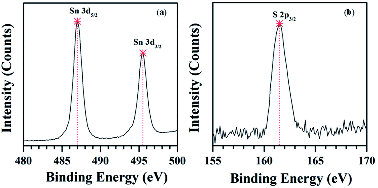 | ||
| Fig. 5 XPS spectra of SnS nanowires grown on Si substrate at the growth temperature of 650 °C: (a) Sn and (b) S elements. | ||
Fig. 6(a) shows the schematic diagram of SnS nanowire FET device, and its typical FESEM image is shown in Fig. 6(b). Current flow through the device (Ids) as a function of applied bias voltage (Vds) measured at different gate voltages (Vg) is shown in Fig. 6(c). It clearly shows that the current flow through the device increases with the decrease of gate voltage from 0 to −5 V, which reflects the well-known gating effect of the p-type semiconductor. Further, as shown in inset of Fig. 6(c), the variation of device current as a function of gate bias voltage (Ids vs. Vg) at a constant Vds of 2.5 V reveals that the SnS nanowires based FET devices consist of an on/off ratio about 103 and a threshold (Vth) voltage of 2.3 V. It implies that the as-grown FET device belongs to depletion mode.
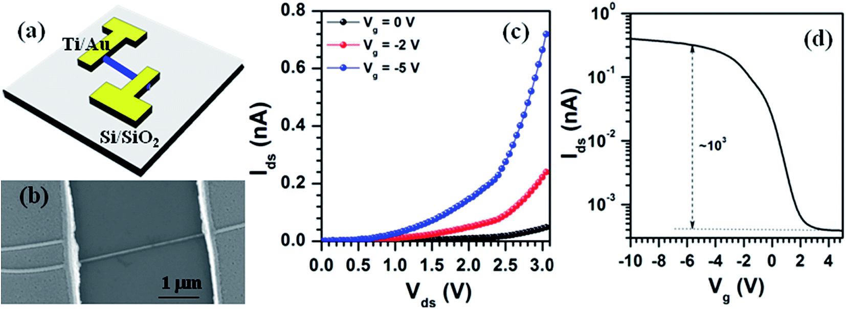 | ||
| Fig. 6 (a) Schematic diagram and (b) FESEM image of SnS nanowire FET device, (c) Ids versus Vds plots measured at different Vg values, and (d) variation of Ids as a function of Vg at a constant Vds of 2.5 V. | ||
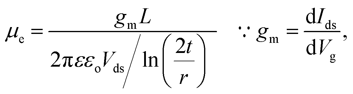
In order to explore the electrical properties of SnS nanowires, we have calculated the carrier concentration (n), field effect mobility (μ), and resistivity (ρ) of the nanowires by using the equations described below.52 The electron concentration (n) of nanowire structures is calculated from the threshold voltage (Vth) of the device by using eqn (1):
 | (1) |
 | (2) |
 | (3) |
| ρ = 1/enμe. | (4) |
Here, we considered Vth at Vg = 0 is 2.3 V, L is 2.5 μm, r of SnS nanowire is 7 nm, ε of SiO2 is ∼3.9, εo is 8.85 × 10⁻¹² F m−1, and t of SiO2 layer is 100 nm. From these calculations, the carrier density, mobility, and resistivity of SnS nanowires are found to be 6.03 × 1018 cm−3, 1.47 × 10⁻² cm2 V−1 s−1, and 70.1 Ω cm, respectively. These values are quite different than that of electrical properties of ultrathin SnS films obtained from the Hall-effect measurements,55 which is probably attributed to phonon scattering and surface roughness of the nanostructures.56
Growth mechanism
In the present study, SnS nanostructures have been realized using gold as catalyst and SnS powder as source. Further, the overall experimental results show that nanostructures grown on either Si or sapphire substrates consist of gold particle as tip, and their diameters are smaller than the diameter of gold particles. These nanowires are single crystalline crystallites, and have a preferential growth direction along the (100) planes. On the other hand, the growth of SnS nanowires is completely independent of the substrate material, since the changes in morphology, density, or the crystal-structure of SnS nanowires grown on sapphire or Si substrates are marginal. Therefore, the plausible growth mechanism of SnS nanowires could be a vapor–liquid–solid (VLS) process, which is schematically represented in Fig. 7. Similar concept has been applied for explaining the growth of gallium arsenide (GaAs) nanowires under VLS growth process.57 As per the Wagner and Ellis demonstration, Au catalyst forms a liquid-alloy particle (eutectic formation) upon chemically reacting with source material supplied in the form of vapor.58 For continuous supply of the source, at above the saturation, the material gets precipitate as solid nanowire at the bottom of the particle, which is schematically represented in Fig. 7(a).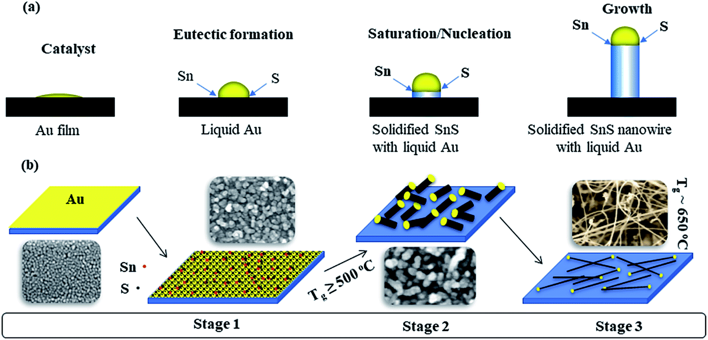 | ||
| Fig. 7 Schematic representation of (a) various steps in VLS growth of SnS nanowires, and (b) SnS nanowires growth at different temperatures: (stage 1) Nncleation of vaporized Sn and S atoms, (stage 2) nano features having Au NP as tip, and (stage 3) growth of long nanowires. | ||
Au deposited substrates consist of granular surface morphology, which uniformly covers the entire substrate (first image in Fig. 7(b)). When the growth temperature was carried out at 500 °C, the formation of SnS–Au structures is observed (@stage 1). It indicates that upon heating, the source SnS powder decomposes as Sn and S, and travels along the tube as a vapor with carrier gas. At above 450 °C, the SnS–Au structures become droplets and act as energetically favored centers for adsorption of Sn and S vapors, since we have noticed flakey films growth over substrates at a growth temperature of 450 °C (see SI11†). The Sn and S vapors accumulate around SnS–Au droplets and forms stable SnS phase via the vapor–liquid–solid (VLS) mechanism when it reaches the supersaturation concentration. Formation of typical SnS crystallites is observed particularly at the growth temperature of 500 °C, Fig. SI3(a) & (b),† (@stage 1). With increase of density of SnS nuclei, SnS crystallizes along its preferential direction, and pushes the gold droplet at above the growth temperature of 500 °C, Fig. SI3(c) & (d),† (@stage 2). Upon increasing the growth temperature, the SnS forms as nanowires, Fig. SI3(e) & (f),† (@stage 3). On the other hand, the presence of atoms on the surface of nanofragments (i.e. button-mushroom shaped crystals) induces compressive stress, and leads to increase in length.59–61 This could be the reason for the growth of longer nanowires under eutectic temperature of SnS and Au. Finally, under an optimum growth temperature (∼650 °C), the formation of ultralong SnS nanowires with uniform morphology is taken place.
Conclusions
The growth of SnS nanostructures was performed on gold catalyst coated sapphire and Si substrates by a chemical vapor deposition at different temperatures varying from 500 to 950 °C. Freestanding high-density SnS nanowires are found at the growth temperature of around 650 °C, which have smooth and uniform surface morphology with thinnest diameter of 13 nm (14 nm in case of Si). These SnS nanowires are single crystalline, and have preferential growth direction along the (100) planes. These structures also consist of nearly stoichiometric chemical composition of its constituents (i.e. the Sn/S atomic% ratio is about 1.13). These interesting results emphasize that the reported methodology for the growth of high quality 1D SnS nanowires allow us to develop various efficient and sustainable SnS based devices, including batteries, solar cells, and field emission devices.Conflicts of interest
There are no conflicts to declare.Acknowledgements
MD and NKR were supported by the World Class University (WCU) program through the National Research Foundation of Korea, funded by the Ministry of Education, Science, and Technology (R31-10026). NKR and SHP wish to acknowledge the partial support of Korean Federation of Science and Technology Societies grant funded by the Korean government (Ministry of Science, ICT and Future Planning) through Brain Pool Fellowship and National Research Foundation of Korea (2014R1A2A1A11053213). Finally, all the authors are highly thankful to Dr Moon, TEM operator, KBSI, Gwangju, for his consistent help in the analysis of our samples.References
- A. S. Arico, P. Bruce, B. Scrosati, J. M. Tarascon and W. Van Schalkwijk, Nat. Mater., 2005, 4, 366–377 CrossRef CAS PubMed.
- M. Frasconi, D. Deriu, A. D'Annibale and F. Mazzei, Nanotechnology, 2009, 20, 505501–505508 CrossRef PubMed.
- V. Baranauskas, M. Fontana, H. J. Ceragioli and A. C. Peterlevitz, Nanotechnology, 2004, 15, S678–S683 CrossRef CAS.
- A. R. Hirst, B. Escuder, J. F. Miravet and D. K. Smith, Angew. Chem., Int. Ed., 2008, 47, 8002–8018 CrossRef CAS PubMed.
- D. Roy, B. Shastri, M. Imamuddin, K. Mukhopadhyay and K. U. B. Rao, Renewable Energy, 2011, 36, 1014–1018 CrossRef CAS.
- D. P. Hansora, N. G. Shimpi and S. Mishra, RSC Adv., 2015, 5, 107716–107770 RSC.
- H. Kafashan, R. Ebrahimi-Kahrizsangi, F. Jamali-Sheini and R. Yousefi, Phys. Status Solidi A, 2016, 213, 1302–1308 CrossRef CAS.
- H. T. Hsu, M. H. Chiang, C. H. Huang, W. T. Lin, Y. S. Fu and T. F. Guo, Thin Solid Films, 2015, 584, 37–40 CrossRef CAS.
- M. Patel and A. Ray, RSC Adv., 2014, 4, 39343–39350 RSC.
- M. Devika, N. K. Reddy, K. Ramesh, K. R. Gunasekhar, E. S. R. Gopal and K. T. R. Reddy, J. Electrochem. Soc., 2006, 153, G727–G733 CrossRef CAS.
- N. K. Reddy, Y. B. Hahn, M. Devika, H. R. Sumana and K. R. Gunasekhar, J. Appl. Phys., 2007, 101, 093522 CrossRef.
- J. J. Loferski, J. Appl. Phys., 1956, 27, 777–784 CrossRef CAS.
- J. J. Cai, Z. S. Li and P. K. Shen, ACS Appl. Mater. Interfaces, 2012, 4, 4093–4098 CAS.
- C. F. Pan and J. Zhu, J. Mater. Chem., 2009, 19, 869–884 RSC.
- G. H. Yue, Y. D. Lin, X. Wen, L. S. Wang, Y. Z. Chen and D. L. Peng, Appl. Phys. A: Mater. Sci. Process., 2012, 106, 87–91 CrossRef CAS.
- A. M. Tripathi and S. Mitra, RSC Adv., 2014, 4, 10358–10366 RSC.
- J. S. Zhu, D. L. Wang and T. F. Liu, Ionics, 2014, 20, 141–144 CrossRef CAS.
- H. Chauhan, M. K. Singh, S. A. Hashmi and S. Deka, RSC Adv., 2015, 5, 17228–17235 RSC.
- D. Das and R. K. Dutta, J. Colloid Interface Sci., 2015, 457, 339–344 CrossRef CAS PubMed.
- Q. Tan, C. F. Wu, W. Sun and J. F. Li, RSC Adv., 2016, 6, 43985–43988 RSC.
- X. Zhou, L. Gan, Q. Zhang, X. Xiong, H. Q. Li, Z. Q. Zhong, J. B. Han and T. Y. Zhai, J. Mater. Chem. C, 2016, 4, 2111–2116 RSC.
- D. D. Vaughn, O. D. Hentz, S. R. Chen, D. H. Wang and R. E. Schaak, Chem. Commun., 2012, 48, 5608–5610 RSC.
- V. S. R. R. Pullabhotla and M. W. Mabila, Mater. Lett., 2016, 183, 30–33 CrossRef CAS.
- J. W. Wang, Y. Y. Lu, N. Zhang, X. D. Xiang, J. Liang and J. Chen, RSC Adv., 2016, 6, 95805–95811 RSC.
- F. Jamali-Sheini, R. Yousefi, N. A. Bakrc, M. Cheraghizade, M. Sookhakian and N. M. Huang, Mater. Sci. Semicond. Process., 2015, 32, 172–178 CrossRef CAS.
- N. K. Reddy, M. Devika, Q. Ahsanulhaq and K. R. Gunasekhar, Cryst. Growth Des., 2010, 10, 4769–4772 Search PubMed.
- N. K. Reddy, M. Devika and K. R. Gunasekhar, Appl. Phys. A: Mater. Sci. Process., 2014, 116, 1193–1197 CrossRef CAS.
- W. S. Gao, C. S. Wu, M. Cao, J. Huang, L. J. Wang and Y. Shen, J. Alloys Compd., 2016, 688, 668–674 CrossRef CAS.
- Q. L. Ren, B. Li, Z. Y. Peng, G. J. He, W. L. Zhang, G. Q. Guan, X. J. Huang, Z. Y. Xiao, L. J. Liao, Y. S. Pan, X. J. Yang, R. J. Zou and J. Q. Hu, New J. Chem., 2016, 40, 4464–4467 RSC.
- E. C. Greyson, J. E. Barton and T. W. Odom, Small, 2006, 2, 368–371 CrossRef CAS PubMed.
- N. K. Reddy, ECS J. Solid State Sci. Technol., 2013, 2, P259–P263 CrossRef CAS.
- N. K. Reddy, M. Devika, M. Prashantha, K. Ramesh and K. R. Gunasekhar, Eur. Phys. J.: Appl. Phys., 2012, 60, 10102 CrossRef.
- R. Rao, H. Chandrasekaran, S. Gubbala, M. K. Sunkara, C. Daraio, S. Jin and A. M. Rao, J. Electron. Mater., 2006, 35, 941–946 CrossRef CAS.
- H. K. Wu, Y. M. Yang, E. Oh, F. C. Lai and D. Yu, Nanotechnology, 2012, 23, 265602 CrossRef PubMed.
- H. X. Tang and H. A. Sodano, Appl. Phys. Lett., 2013, 102, 063901 CrossRef.
- A. I. Martinez-Banderas, A. Aires, F. J. Teran, J. E. Perez, J. F. Cadenas, N. Alsharif, T. Ravasi, A. L. Cortajarena and J. Kosel, Sci. Rep., 2016, 6, 35786 CrossRef CAS PubMed.
- M. Simanullang, K. Usami, T. Kodera, K. Uchida and S. Oda, J. Nanosci. Nanotechnol., 2011, 11, 8163–8168 CrossRef CAS PubMed.
- P. Prete and N. Lovergine, MOVPE Self-Assembly and Physical Properties of Free-Standing III–V Nanowires, 2010 Search PubMed.
- V. Consonni, V. G. Dubrovskii, A. Trampert, L. Geelhaar and H. Riechert, Phys. Rev. B: Condens. Matter Mater. Phys., 2012, 85, 155313 CrossRef.
- T. F. Li, Y. H. Chen, W. Lei, X. L. Zhou, S. Luo, Y. Z. Hu, L. J. Wang, T. Yang and Z. G. Wang, Nanoscale Res. Lett., 2011, 6, 463 CrossRef PubMed.
- K. Seo, J. Bong, J. W. Kim, Y. H. Song, Y. H. Shin, Y. Kim and S. Ju, J. Nanomater., 2015, 2015, 201420 Search PubMed.
- N. K. Reddy, M. Devika and E. S. R. Gopal, Crit. Rev. Solid State Mater. Sci., 2015, 40, 359–398 CrossRef.
- C. H. An, K. B. Tang, G. Z. Shen, C. R. Wang, Q. Yang, B. Hai and Y. T. Qian, J. Cryst. Growth, 2002, 244, 333–338 CrossRef CAS.
- D. Chen, G. Z. Shen, K. B. Tang, S. J. Lei, H. G. Zheng and Y. T. Qian, J. Cryst. Growth, 2004, 260, 469–474 CrossRef CAS.
- J. Zhou, Y. Ding, S. Z. Deng, L. Gong, N. S. Xu and Z. L. Wang, Adv. Mater., 2005, 17, 2107–2110 CrossRef CAS.
- S. R. Suryawanshi, S. S. Warule, S. S. Patil, K. R. Patil and M. A. More, ACS Appl. Mater. Interfaces, 2014, 6, 2018–2025 CAS.
- G. H. Yue, Y. D. Lin, X. Wen, L. S. Wang and D. L. Peng, J. Mater. Chem., 2012, 22, 16437–16441 RSC.
- M. X. Wang, G. H. Yue, Y. D. Lin, X. Wen, D. L. Peng and Z. R. Geng, Nano-Micro Lett., 2013, 5, 1–6 CrossRef CAS.
- H. X. Zhang, J. P. Ge, J. Wang and Y. D. Li, Nanotechnology, 2006, 17, S253–S261 CrossRef CAS.
- J. P. Ge, J. Wang, H. X. Zhang and Y. D. Li, Chem.–Eur. J., 2004, 10, 3525–3530 CrossRef CAS PubMed.
- J. P. Ge, J. Wang, H. X. Zhang, X. Wang, Q. Peng and Y. D. Li, Adv. Funct. Mater., 2005, 15, 303–308 CrossRef CAS.
- J. Goldberger, D. J. Sirbuly, M. Law and P. Yang, J. Phys. Chem. B, 2005, 109, 9–14 CrossRef CAS PubMed.
- O. Wunnicke, Appl. Phys. Lett., 2006, 89, 083102 CrossRef.
- W. Q. Yang, L. Dai, R. M. Ma, C. Liu, T. Sun and G. G. Qin, Appl. Phys. Lett., 2008, 93, 033102 CrossRef.
- M. Devika, N. K. Reddy and K. R. Gunasekhar, Thin Solid Films, 2011, 520, 628–632 CrossRef CAS.
- E. B. Ramayya, D. Vasileska, S. M. Goodnick and I. Knezevic, IEEE Trans. Nanotechnol., 2007, 6, 113–117 CrossRef.
- V. G. Dubrovskii, Semicond. Semimetals, 2015, 93, 1–78 Search PubMed.
- R. S. Wagner and W. C. Ellis, Appl. Phys. Lett., 1964, 4, 89–90 CrossRef CAS.
- R. Agrawal, B. Peng, E. E. Gdoutos and H. D. Espinosa, Nano Lett., 2008, 8, 3668–3674 CrossRef CAS PubMed.
- J. J. Lao, M. N. Tam, D. Pinisetty and N. Gupta, JOM, 2013, 65, 175–184 CrossRef CAS.
- S. J. A. Koh and H. P. Lee, Nanotechnology, 2006, 17, 3451–3467 CrossRef CAS PubMed.
Footnotes |
| † Electronic supplementary information (ESI) available: Under this section a few details about the experimental setup, surface morphology of catalyst layers over substrates, FESEM images, EDS analysis, and surface morphology of SnS films are provided. See DOI: 10.1039/c7ra06346f |
| ‡ Authors have equal contribution. |
| This journal is © The Royal Society of Chemistry 2017 |