
 Open Access Article
 This Open Access Article is licensed under a
 Creative Commons Attribution 3.0 Unported Licence
Electric field tunable band-gap crossover in black(blue) phosphorus/g-ZnO van der Waals heterostructures†
Wei Zhang ab and
Lifa Zhang*a
ab and
Lifa Zhang*a
aDepartment of Physics and Institute of Theoretical Physics, Jiangsu Provincial Key Laboratory for Numerical Simulation of Large Scale Complex Systems, Nanjing Normal University, Nanjing 210023, China. E-mail: phyzlf@njnu.edu.cn
bPhysicochemical Group of Department of Criminal Science and Technology, Nanjing Forest Police College, Nanjing 210023, China
First published on 11th July 2017
Abstract
Electrically controlled band-gaps and efficient carrier confinement or separation are crucial in the design of nanoscale light-emitting and photoelectric devices. Here, using hybrid density functional calculations, we studied the electronic and optical properties of graphitic zinc oxide (g-ZnO) and phosphorene van der Waals (vdW) heterostructures. We found that although black(blue) phosphorus/g-ZnO shows an intrinsic type-I(type-II) band alignment with a direct(indirect) band-gap, a vertical electric field can induce type-I-to-type-II transition for the black phosphorus/g-ZnO, and the band edges of blue phosphorus/g-ZnO can be electrically modulated to obtain a direct band-gap at the Γ point. Intriguingly, the heterostructures also showed improved visible-UV light adsorption compared with the single-layers. Our findings reveal that g-ZnO can be used not only as a capping layer to protect the electronic characteristics of phosphorene, but also as the active layer to tune the electronic and optical properties of phosphorene, which may promote potential phosphorene-based applications in the future.
1 Introduction
Since the successful exfoliation of graphene,1,2 two-dimensional (2D) materials such as single-layer (1L) transition metal dichalcogenides (TMDs)3,4 have attracted great attention because of the peculiar physics brought about by them and their potential for the next generation of nanoscale device applications.3–5 Recently, a new elemental 2D material called black phosphorus (black-p) has been fabricated by several research groups.6–8 Unlike semimetallic graphene and the typical 1L-TMD MoS2, which both exhibit low electron carrier mobility5,9,10 (10–200 cm2 V−1 s−1), black-p has many fascinating properties such as a finite direct band-gap (Eg) and high electron mobility (1000 cm2 V−1 s−1) at room temperature.11,12 Very recently the theoretically-predicted blue phosphorus (blue-p),13 which is an allotrope of phosphorene, was successfully synthesized.14 Theoretical calculations indicated that blue-p has a wider Eg and a higher hole mobility (1700 cm2 V−1 s−1) than black-p.15,16Despite these advantages of phosphorene, black-p and blue-p have poor structural stability at ambient conditions in the presence of water and oxygen molecules.17–20 Enhanced stability was reported in few-layer black-p flakes, which were passivated by Al2O3.21,22 The multilayer black-p was predicted to demonstrate better stability than its 1L counterpart.23 In this sense, chemically stable 2D materials can be considered as capping layers to protect phosphorene from ambient degradation.24,25
Zinc oxide (ZnO) is a key technological material which is well known for its versatile properties and applications in photocatalysts,26 solar cells,27 piezoelectrics,28 etc. Graphitic zinc oxide (g-ZnO) is the 2D form of bulk ZnO.29–31 Compared with bulk ZnO, little is known about g-ZnO although it has been confirmed experimentally for several years.29 Importantly, previous theoretical and experimental works have shown that g-ZnO is chemically stable.29–31 Yao et al. found that g-ZnO is a suitable substrate for graphene in real applications.32 A natural question arises: can g-ZnO be used to protect the intrinsic electronic properties of phosphorene? Van der Waals (vdW) heterostructures based on the integration of 2D materials have presented abundant opportunities for applications in light-emitting33,34 and photoelectric devices.35,36 In the design of these devices, the electrically controlled Eg and efficient carrier confinement or separation are crucial.34,35,37 However, the Eg type and band alignment are usually fixed,38–41 e.g., black-p/MoS238 and black-p/blue-p,39 which limits the multifunctionality of the devices. Considering that the heterostructures are often subjected to an electric field (E) when applied to nano-electronic devices, another question arises: can black(blue)-p/g-ZnO vdW heterostructures have electrically tunable electronic properties for the above applications?
2 Computational methods
First-principles calculations were performed using the VASP code42,43 with the PAW method.44 We approximated the exchange–correlation potential with the PBE functional.45 A plane-wave cutoff of 750 eV was used throughout. 14 × 2 × 2(16 × 16 × 1) k-point meshes46 were used for the black-p(blue-p)/g-ZnO heterostructures. Using these parameters, an energy convergence of less than 0.015 meV per atom was achieved.47 The crystal structures were relaxed until the inter-atomic forces were smaller than 0.01 eV Å−1. A vacuum space of 15 Å was used in the direction normal to the layers. The vdW-DF method was used to describe the vdW interactions.48 Since the Eg is usually underestimated by DFT, e.g., the PBE calculated Eg of black-p is 0.93 eV while the experimental value is 1.45 eV,49 the electronic and optical properties were calculated using the HSE06 hybrid functional.503 Results and discussion
We first obtained the equilibrium structures of black-p, g-ZnO and blue-p. As shown in Fig. 1(a), the calculated lattice constants of black-p, g-ZnO and blue-p were a1(b1) = 3.299(4.613) Å, a2 = 3.289 Å and a3 = 3.278 Å, respectively, which agreed well with previous theoretical and experimental values.14,29–31,39 To construct blue-p/g-ZnO, the lattice constant was set to 3.283 Å so that the maximum lattice mismatch was just 0.16%. For black-p/g-ZnO, we first changed the primitive cell of g-ZnO to a rectangle unit cell with a2 = 3.289 Å and b′2 = 5.696 Å, then the heterostructure consisted of a 1 × 5 × 1 primitive cell of black-p and a 1 × 4 × 1 rectangle unit cell of g-ZnO. The lattice constants of black-p/g-ZnO were a = 3.294 Å and b = 22.925 Å and the maximum lattice mismatches were only Δa = 0.15% and Δb = 0.62%. Thus, g-ZnO had well-matched lattice constants with respect to black(blue)-p.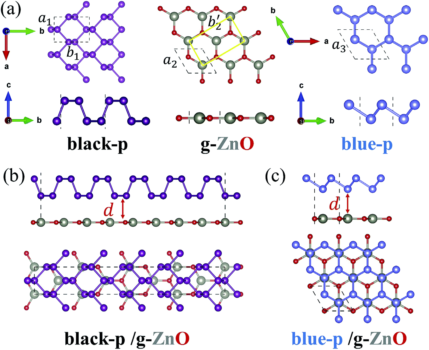 | ||
| Fig. 1 The top view (upper panel) and side view (lower panel) of (a) the three single layers, (b) black-p/g-ZnO and (c) blue-p/g-ZnO. The dotted lines in (a) denote the primitive cells. The yellow solid lines in (a) denote the rectangle unit cell of g-ZnO. The dotted lines in (b) and (c) denote the heterostructures. | ||
To get the most stable black-p/g-ZnO, we moved the black-p along the armchair direction while the g-ZnO was kept fixed. Meanwhile, the relative displacement between the black-p and g-ZnO along the zigzag direction was considered. Then we relaxed all the possible patterns of heterostructures and obtained the corresponding total energies. For blue-p/g-ZnO there were AA, AB and C patterns.51 Other typical patterns are provided in the ESI†.47 The most stable patterns are shown in Fig. 1(b) and (c). We found that the AB pattern, where the lower P atoms were just above the Zn atoms, was the most stable pattern of the blue-p/g-ZnO, which is similar to the case of h-BN/graphene.51 In the relaxed structure of isolated g-ZnO, the Zn and O atoms formed a hexagonal plane,32 which could also be seen in the blue-p/g-ZnO. In the black-p/g-ZnO however, the Zn and O atoms had little buckling height (hZn–O) along the c direction even when we relaxed the black-p/g-ZnO without fixing the in-plane lattice constants. The maximum hZn–O (0.34 Å) we achieved was within the scope of the experimental value,29 where the g-ZnO grown on Ag(111) showed a hZn–O of 0.12–0.58 Å. Besides, the average hZn–O of the black-p/g-ZnO was just 0.007 Å. The calculated Egs of the isolated g-ZnO without hZn–O and that with hZn–O in the black-p/g-ZnO were 3.29 and 3.27 eV, respectively, suggesting that the very small strain and the hZn–O have negligible effects on the electronic properties.
The interlayer distance (d) of the black(blue)-p/g-ZnO was 3.23(3.44) Å. The binding energy (Eb) of the black(blue)-p/g-ZnO, which was calculated by Eb = E[black(blue)-p/g-ZnO] − E[black(blue)-p] − E(g-ZnO), was 34.82(23.55) meV per atom. Note that different strategies in describing the vdW interactions often lead to marked differences in quantifying the Eb(d). The predicted Eb(d) of black-p/g-ZnO was 43.32(3.09), 50.23(2.95) and 52.39(2.79) meV per atom (Å) by optPBE,52 optB88 (ref. 52) and DFT+D3,53 respectively. OptPBE, optB88 and DFT+D3 predicted that the Eb(d) of blue-p/g-ZnO was 31.98(3.2), 38.79(3.09) and 40.67(2.86) meV per atom (Å), respectively. Clearly, all the vdW functionals employed here gave qualitatively consistent results about the relative amplitude relation of Eb(d) for the two heterostructures, i.e., the black-p/g-ZnO had a larger (lower) Eb(d) than the blue-p/g-ZnO. Besides, other main conclusions (e.g., the most stable patterns of heterostructures and the electric field induced Eg crossover) were also not affected by the choice of vdW functional. Therefore, in what follows we just show the results using vdW-DF.48 The Eb(d) values obtained by other vdW functionals can be used as references for experimental measurements. As shown in Fig. 2(a), the black-p/g-ZnO displayed a direct Eg of 1.38 eV, and both the valence band maximum (VBM) and conduction band minimum (CBM) were located at the Γ point. Whereas blue-p/g-ZnO showed an indirect Eg of 2.26 eV, and the VBM was located at the Γ point while the CBM lay between the Γ and M points. Compared with isolated black(blue)-p (Fig. S3†), the direct(indirect) Eg character of black(blue)-p was kept and the Eg of black/g-ZnO was nearly unchanged, while the Eg of blue/g-ZnO decreased to 2.26 eV. To understand this, the band structures of black-p(blue)/g-ZnO were projected to their components. We can see that both the VBM and CBM of black-p/g-ZnO were contributed by black-p, suggesting the type-I heterostructure. For blue-p/g-ZnO, the VBM was contributed by g-ZnO while the CBM was distributed on blue-p, indicating the type-II heterostructure. From Fig. 2(a) and S3,† we can also see the main energy-band dispersion of isolated blue-p in blue/g-ZnO. Thus, the above results imply that g-ZnO can be used as a potential capping layer to protect the main electronic characters of phosphorene, especially black-p. The band alignments of heterostructures are even more important than the band structures in material and device design. Type-I band alignment of black-p/g-ZnO can facilitate the radiative recombination of holes and electrons, which is desirable in light-emitting applications.33 Type-II band alignment of blue-p/g-ZnO is one of the key factors for the efficient separation of photogenerated electron–hole pairs, which can increase the carriers’ lifetime and is desired for applications in photodetection and photovoltaics.35,36 The photogenerated electrons of g-ZnO can be easily transferred to the CB of blue-p while the photogenerated holes of blue-p have the counter movement, i.e., from blue-p to the VBM of g-ZnO. As a result, the energy-wasted electron–hole recombination could be greatly reduced. We can gain further insight from the band decomposed charge densities of VBM(CBM). As shown in the inset of Fig. 2(a), all the charge carriers are confined in the black-p, while the lowest-energy electrons and holes of blue-p/g-ZnO are spatially localized on the blue-p and g-ZnO, respectively. Another key factor which efficiently separates the electrons and holes is the large built-in electric field (E). Thus we plotted the average in-plane electrostatic potential of blue-p/g-ZnO. Fig. 2(b) clearly shows the significant potential difference at the interface region, indicating the large built-in E, which promotes the transition of electrons(holes). The transfer of carriers can also be seen from the differential charge density (eqn S4†). As shown in Fig. 2(c), the negative(positive) values denote the accumulation of electrons(holes) at the blue-p(g-ZnO), indicating that the p-type g-ZnO and n-type blue-p form a type-II p–n heterostructure.
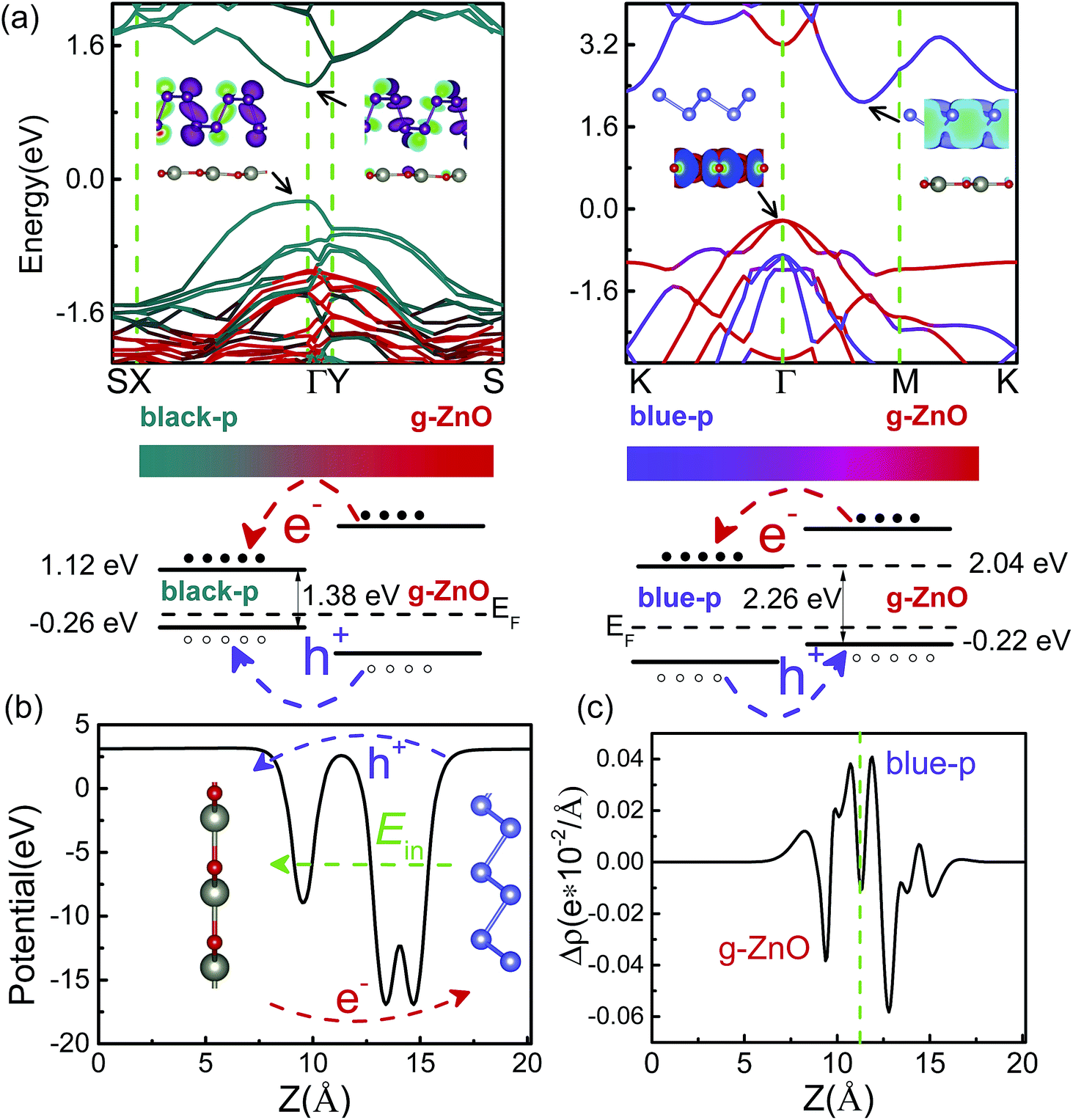 | ||
| Fig. 2 (a) The band structures of black-p/g-ZnO (left panel) and blue-p/g-ZnO (right panel). The color scales denote the contributions from the single layers. Inset is the band decomposed charge density of VBM(CBM). The isosurface value is 0.001 e− bohr−3. Schematics of the band alignments are also shown. (b) The average electrostatic potential and (c) differential charge density of blue-p/g-ZnO along the z direction. Ein is the built-in electric field. The negative(positive) values of Δρ denote the gain(loss) of electrons. | ||
As an efficient photoelectric device, it should absorb as much visible-UV light as possible. Thus we studied the optical absorption by calculating the frequency dependent dielectric function in the independent-particle picture. As shown in Fig. 3, the black-p/g-ZnO exhibited stronger visible-UV light absorption than its components, especially in the energy range of ∼2.12 to 5 eV. The blue-p/g-ZnO showed a wider absorption range and overall stronger visible-UV light absorption in the energy range of ∼2.4 to 4.5 eV. The enhanced optical absorption can be understood from the interlayer coupling and charge transfer in the heterostructures, where the electronic states overlap and the new optical transitions are induced.
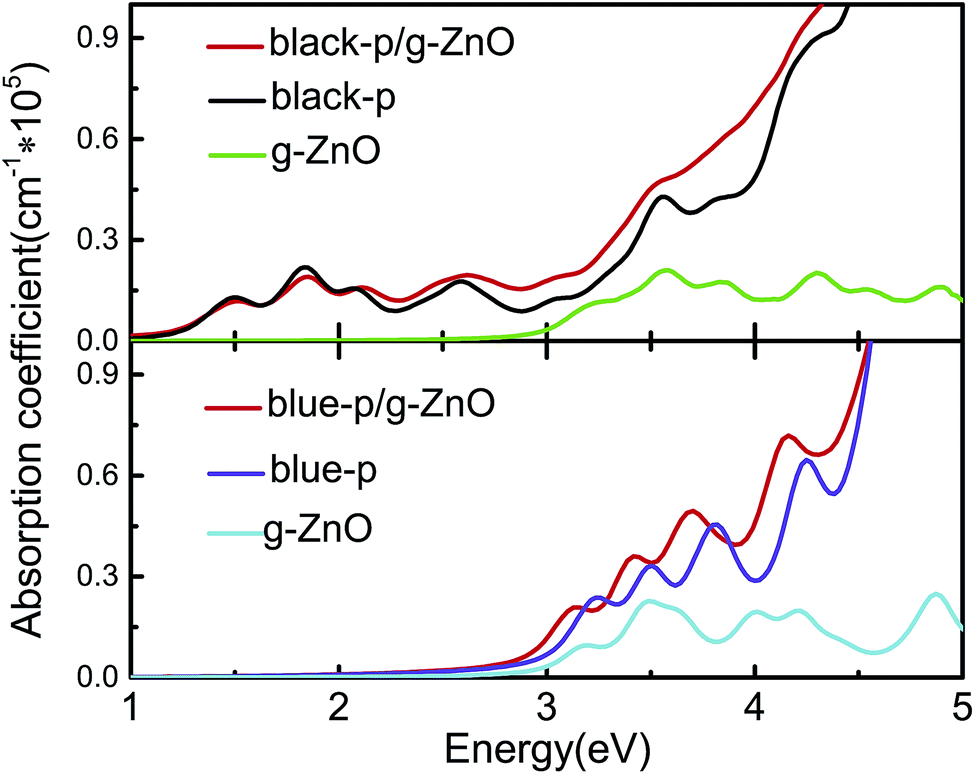 | ||
| Fig. 3 Absorption coefficients of black(blue)-p/g-ZnO and the components. The imaginary parts of the dielectric functions are averaged over all the directions. | ||
Finally, we will discuss the effect of E on the electronic properties. A positive E from black(blue)-p to g-ZnO is introduced. Table 1 shows the structural information of heterostructures without external E and with E = 1.2 V Å−1. It was found that the relaxed bond lengths and bond angles were hardly affected by the E. Only the interlayer distances had relatively small changes. Besides, the band-gaps of black-p/g-ZnO and blue-p/g-ZnO at E = 1.1 V Å−1 were 1.16 and 1.24 eV, respectively, indicating the character of semiconductors. Therefore, our results show that the structures of the heterostructures were still undamaged in such a strong electric field.54–57
| E | d | P–P | Zn–O | P–P–P | Zn–O–Zn |
|---|---|---|---|---|---|
| Black-p/g-ZnO | |||||
| 0 | 3.23 | 2.26 | 1.91 | 103.42 | 120.04 |
| 1.2 | 3.26 | 2.25 | 1.91 | 103.29 | 119.78 |
![[thin space (1/6-em)]](https://www.rsc.org/images/entities/char_2009.gif) |
|||||
| Blue-p/g-ZnO | |||||
| 0 | 3.44 | 2.27 | 1.9 | 92.66 | 120 |
| 1.2 | 3.54 | 2.27 | 1.9 | 92.63 | 119.49 |
As seen in Fig. 4(a) and (b), the E initially exerted little influence on the Eg of black-p/g-ZnO. This is because both the VBM and CBM of black-p were nearly unchanged at first. In contrast to black-p, the VBM and CBM of g-ZnO linearly increased with E when the E was less than 0.8 V Å−1. Thus the energy difference between the VBM of black-p and the VBM of g-ZnO gradually decreased. The VBM of black-p began to decrease at E = 0.8 V Å−1, while the VBM of g-ZnO continued to increase with E. When the E increased to 1.1 V Å−1, the VBM of g-ZnO became the VBM of the black-p/g-ZnO. This can be clearly seen in Fig. 4(a) (E = 1.1 V Å−1), where g-ZnO played the dominant role for the contributions of VBs around the Fermi level and the VBM was fully occupied by the O-px and Zn-dxy states of g-ZnO. At the same time, the CBM of the black-p/g-ZnO was still contributed by the black-p, thus type-I-to-type-II Eg crossover occurred. From Fig. 4(c) we can see the lowest-energy electrons and holes located at different layers.
 | ||
| Fig. 4 (a) The effect of E on the band structures of black-p/g-ZnO. (b) The evolution of VBM(CBM) of black-p/g-ZnO with E. The Fermi level is set as zero. (c) The band decomposed charge density of VBM(CBM) of black-p/g-ZnO at E = 1.1 V Å−1. The arrows denote the direction of the vertical electric field. The color scales denote the contributions from the single layers. The isosurface value is 0.001 e− bohr−3. | ||
As shown in Fig. 5 and S5,† the Eg of blue-p/g-ZnO linearly decreased with increasing E, showing a giant Stark effect. The indirect gap character and type-II band alignment were not affected by the E at first. However, the CBM of blue-p shifted to the Γ point when the E increased to 1.1 V Å−1, forming the direct Eg. The indirect-to-direct transition of Eg was greatly beneficial to the transition of photogenerated electrons from the VBM of g-ZnO to the CBM of blue-p as the momentum was preserved in this process. When the E increased to 1.2 V Å−1, the Eg sharply reduced to nearly zero (0.08 eV), but the direct Eg character was kept. It was expected that the blue-p/g-ZnO would be a metal when the E increased further. This is different from the case of black-p/g-ZnO, which was still a semiconductor at E = 1.2 V Å−1. Notably, the Ein and E had the same potential direction and the interlayer coupling was enhanced when the external E was introduced, which can be clearly seen in Fig. 6. The enhanced interaction can offer improved carrier separation performance in blue-p/g-ZnO.
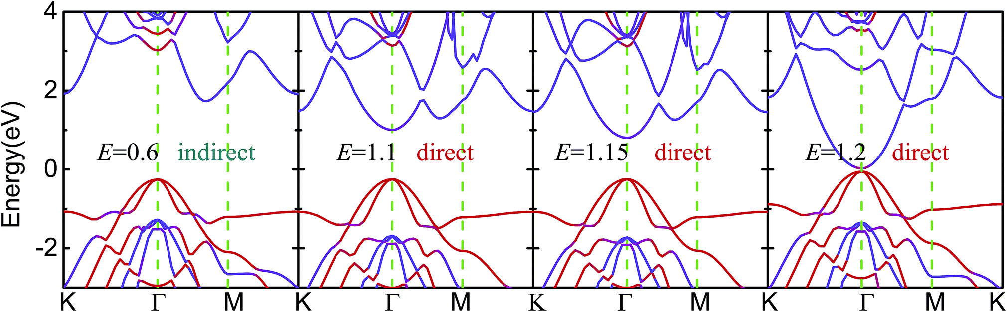 | ||
| Fig. 5 The effect of E on the band structures of blue-p/g-ZnO. The color scales denote the contributions from the single layers. The “direct” and “indirect” denote the types of Eg. | ||
 | ||
| Fig. 6 The effect of E on the differential charge density of blue-p/g-ZnO. | ||
4 Conclusion
In summary, we have theoretically studied the electronic and optical properties of vdW heterostructures black(blue)-p/g-ZnO by means of hybrid density functional calculations. Although the black(blue) phosphorus/g-ZnO is found to show an intrinsic type-I(type-II) band alignment with direct(indirect) band-gap, a vertical electric field can induce a type-I-to-type-II transition for the black phosphorus/g-ZnO and modulate the band edges of blue phosphorus/g-ZnO to get a direct band-gap at the Γ point. Moreover, improved visible-UV light absorption is demonstrated in the heterostructures. Our results indicate that g-ZnO can be used not only as a capping layer to protect the electronic characteristics of phosphorene, but also as an active layer to tune the electronic and optical properties of phosphorene.Acknowledgements
Wei Zhang thanks Dr Weixiao Ji, Prof. Xianqi Dai and Dr Yaqiang Ma for their help. We acknowledge the support from the Basic Research Project of Central University (LGYB201715), the National Natural Science Foundation of China (11574154) and the open project (201702) of Jiangsu Provincial Key Laboratory for Numerical Simulation of Large Scale Complex Systems.References
- K. S. Novoselov, A. K. Geim, S. V. Morozov, D. Jiang, Y. Zhang, S. V. Dubonos, I. V. Grigorieva and A. A. Firsov, Science, 2004, 306, 666 CrossRef CAS PubMed.
- K. S. Novoselov, A. K. Geim, S. V. Morozov, D. Jiang, M. I. Katsnelson, I. V. Grigorieva, S. V. Dubonos and A. A. Firsov, Nature, 2005, 438, 197 CrossRef CAS PubMed.
- Q. H. Wang, K. Kalantar-Zadeh, A. Kis, J. N. Coleman and M. S. Strano, Nat. Nanotechnol., 2012, 7, 699 CrossRef CAS PubMed.
- T. Heine, Acc. Chem. Res., 2015, 48, 65 CrossRef CAS PubMed.
- K. S. Novoselov, D. Jiang, T. J. Booth, W. Khotkevich, S. V. Morozov and A. K. Geim, Proc. Natl. Acad. Sci. U. S. A., 2005, 102, 10451 CrossRef CAS PubMed.
- L. K. Li, Y. J. Yu, G. J. Ye, Q. Q. Ge, X. D. Ou, H. Wu, D. L. Feng, X. H. Chen and Y. B. Zhang, Nat. Nanotechnol., 2014, 9, 372 CrossRef CAS PubMed.
- A. Castellanos, et al., 2D Mater., 2014, 1, 025001 CrossRef.
- H. Liu, A. T. Neal, Z. Zhu, Z. Luo, X. F. Xu, D. Tománek and P. D. Ye, ACS Nano, 2014, 8, 4033 CrossRef CAS PubMed.
- B. Radisavljevic, A. Radenovic, J. Brivio, V. Giacometti and A. Kis, Nat. Nanotechnol., 2011, 6, 147 CrossRef CAS PubMed.
- M. S. Fuhrer and J. Hone, Nat. Nanotechnol., 2013, 8, 146 CrossRef CAS PubMed.
- S. P. Koenig, R. A. Doganov, H. Schmidt, A. C. Neto and B. Özyilmaz, Appl. Phys. Lett., 2014, 104, 103106 CrossRef.
- F. Schwierz, Nat. Nanotechnol., 2010, 5, 487 CrossRef CAS PubMed.
- Z. Zhu and D. Tománek, Phys. Rev. Lett., 2014, 112, 176802 CrossRef PubMed.
- J. L. Zhang, S. T. Zhao, C. Han, Z. Z. Wang, S. Zhong, S. Sun, R. Guo, X. Zhou, C. D. Gu, K. D. Yuan, Z. Y. Li and W. Chen, Nano Lett., 2016, 16, 4903 CrossRef CAS PubMed.
- B. Ghosh, S. Nahas, S. Bhowmick and A. Agarwal, Phys. Rev. B: Condens. Matter Mater. Phys., 2015, 91, 115433 CrossRef.
- J. Xiao, M. Q. Long, X. J. Zhang, J. Ouyang, H. Xu and Y. L. Gao, Sci. Rep., 2015, 5, 09961 CrossRef CAS PubMed.
- X. Liu, J. D. Wood, K. S. Chen, E. Cho and M. C. Hersam, J. Phys. Chem. Lett., 2015, 6, 773 CrossRef CAS PubMed.
- J. O. Island, G. A. Steele, H. S. J. van der Zant and A. Castellanos-Gomez, 2D Mater., 2015, 2, 011002 CrossRef.
- G. X. Wang, W. J. Slough, R. Pandey and S. P. Karna, 2D Mater., 2016, 3, 025011 CrossRef.
- Y. Zhao, et al., Angew. Chem., Int. Ed., 2016, 55, 5003 CrossRef CAS PubMed.
- J. Na, Y. T. Lee, J. A. Lim, D. K. Hwang, G. T. Kim, W. K. Choi and Y. W. Song, ACS Nano, 2014, 8, 11753 CrossRef CAS PubMed.
- X. Luo, J. C. M. Hwang, H. Liu, Y. Du and P. D. Ye, IEEE Electron Device Lett., 2014, 35, 1314 CrossRef.
- Y. Q. Cai, G. Zhang and Y. W. Zhang, Sci. Rep., 2014, 4, 6677 CrossRef CAS PubMed.
- Y. Shi, et al., Nano Lett., 2012, 12, 2784 CrossRef CAS PubMed.
- G. R. Berdiyorov, M. Neek-Amal, F. M. Peeters and A. C. T. van Duin, Phys. Rev. B: Condens. Matter Mater. Phys., 2014, 89, 024107 CrossRef.
- K. Maeda, T. Takata, M. Hara, N. Saito, Y. Inoue, H. Kobayashi and K. Domen, J. Am. Chem. Soc., 2005, 127, 8286 CrossRef CAS PubMed.
- M. Law, L. E. Greene, J. C. Johnson, R. Saykally and P. Yang, Nat. Mater., 2005, 4, 455 CrossRef CAS PubMed.
- S. J. Chang, T. J. Hsueh, I. C. Chen and B. R. Huang, Nanotechnology, 2008, 19, 175502 CrossRef PubMed.
- C. Tusche, H. L. Meyerheim and J. Kirschner, Phys. Rev. Lett., 2007, 99, 1026102 CrossRef PubMed.
- H. T. Quang, A. Bachmatiuk, A. Dianat, F. Ortmann, J. Zhao, J. H. Warner, J. Eckert, G. Cunniberti and M. H. Rümmeli, ACS Nano, 2015, 9, 11408 CrossRef CAS PubMed.
- J. Lee, D. C. Sorescu and X. Deng, J. Phys. Chem. Lett., 2016, 7, 1335 CrossRef CAS PubMed.
- Q. S. Yao, Y. Z. Liu, R. F. Lu, C. Y. Xiao, K. M. Deng and E. J. Kan, RSC Adv., 2014, 4, 17478 RSC.
- Z. H. Lu, D. J. Lockwood and J. M. Baribeau, Nature, 1995, 378, 258 CrossRef CAS.
- X. W. Gong, et al., Nat. Photonics, 2016, 10, 253 CrossRef CAS.
- Z. Wang, H. Yin, C. Jiang, M. Safdar and J. He, Appl. Phys. Lett., 2012, 10, 253109 CrossRef.
- F. Wang, Z. X. Wang, K. Xu, F. M. Wang, Q. S. Wang, Y. Huang, L. Yin and J. He, Nano Lett., 2015, 15, 7558 CrossRef CAS PubMed.
- J. Kim, et al., Science, 2015, 349, 723 CrossRef CAS PubMed.
- L. Huang, Y. Li, Z. M. Wei and J. B. Li, Sci. Rep., 2015, 5, 16448 CrossRef CAS PubMed.
- L. Huang and J. B. Li, Appl. Phys. Lett., 2016, 108, 083101 CrossRef.
- W. Y. Yu, Z. L. Zhu, S. L. Zhang, X. L. Cai, X. Wang, C. Y. Niu and W. B. Zhang, Appl. Phys. Lett., 2016, 109, 103104 CrossRef.
- P. Chen, et al., Nanoscale, 2016, 8, 3254 RSC.
- G. Kresse and J. Furthmüller, Phys. Rev. B: Condens. Matter Mater. Phys., 1996, 54, 11169 CrossRef CAS.
- G. Kresse and D. Joubert, Phys. Rev. B: Condens. Matter Mater. Phys., 1999, 59, 1758 CrossRef CAS.
- P. E. Blöchl, Phys. Rev. B: Condens. Matter Mater. Phys., 1994, 50, 17953 CrossRef.
- J. P. Perdew, K. Burke and M. Ernzerhof, Phys. Rev. Lett., 1997, 78, 1396 CrossRef CAS.
- H. J. Monkhorst and J. D. Pack, Phys. Rev. B: Condens. Matter Mater. Phys., 1976, 13, 5188 CrossRef.
- See ESI.†.
- M. Dion, H. Rydberg, E. Schroder, D. C. Langreth and B. I. Lundqvist, 2D Mater., 2004, 92, 246401 CAS.
- H. Liu, et al., ACS Nano, 2014, 8, 4033 CrossRef CAS PubMed.
- J. Heyd, G. E. Scuseria and M. Ernzerhof, J. Chem. Phys., 2006, 124, 219906 CrossRef.
- Y. C. Fan, M. W. Zhao, Z. H. Wang, X. J. Zhang and H. Y. Zhang, Appl. Phys. Lett., 2011, 98, 083103 CrossRef.
- J. Klimeš, D. R. Bowler and A. Michaelides, Phys. Rev. B: Condens. Matter Mater. Phys., 2011, 83, 195131 CrossRef.
- S. Grimme, J. Antony, S. Ehrlich and S. Krieg, J. Chem. Phys., 2010, 132, 154104 CrossRef PubMed.
- G. X. Wang, R. Pandey and S. P. Karnab, Nanoscale, 2015, 7, 524 RSC.
- I. Choudhuri, P. Garga and B. Pathak, J. Mater. Chem. C, 2015, 4, 8253 RSC.
- J. Zhou, Q. Wang, Q. Sun, Y. Kawazoe and P. Jena, Phys. Chem. Chem. Phys., 2015, 17, 17182 RSC.
- D. Nafday, M. Kabir and T. Saha-Dasgupta, Phys. Rev. B, 2016, 93, 045433 CrossRef.
Footnote |
| † Electronic supplementary information (ESI) available. See DOI: 10.1039/c7ra06097a |
| This journal is © The Royal Society of Chemistry 2017 |