 Open Access Article
Tuning the fluorescence intensity and stability of porous silicon nanowires via mild thermal oxidation†
Lu Gan,
Haiping He *,
Qianqian Yu and
Zhizhen Ye
State Key Laboratory of Silicon Materials, School of Materials Science and Engineering, Zhejiang University, Hangzhou 310027, People's Republic of China. E-mail: hphe@zju.edu.cn
First published on 11th July 2017
Abstract
Photoluminescence studies are carried out on porous silicon nanowires (Si NWs) undergoing rapid thermal oxidation. Despite maintaining porosity, the oxidized Si NWs fail to hold the efficient orange photoluminescence even under mild oxidation conditions. However, their PL stability in both air and ethanol achieves significant improvement after proper thermal oxidation.
Introduction
Silicon (Si), pioneer of the current information age, keeps competitive in high-performance integrated devices. Because of its unique structure,1–3 intriguing physicochemical properties,4–6 and potential applications in a vast array of fields,7–10 low-dimensional Si nanostructures have been actively investigated in the past two decades. Among these, porous silicon Si NWs have received significant attention due to their strong quantum confinement,11,12 electrical and luminescent nature,13,14 and simple fabrication.15 To date, much effort has been devoted to realize their morphology control,16,17 understand their photoluminescence (PL) origin,12,18,19 and achieve performance improvements.20,21 Previously, we have demonstrated the feasibility of tuning PL of porous Si nanowires by morphology control,22 revealed interesting temperature-dependent PL properties,23 and managed luminescence and sensing stability enhancement by surface passivation.21Moreover, research on SiOx–Si interface is always a classical topic from both technological and scientific aspects.24–27 Oxidation of Si to form Si–SiOx (usually SiO2) interface occurs easily on the surface of Si NWs either during synthesis or exposure to air. As an excellent insulator, the SiO2 layer passivates the surface of Si, not only by creating a brilliant barrier against a variety of harsh environments (i.e., impurity diffusion), but also by affecting the physicochemical properties of Si NWs. Generally, oxidation of Si NWs is accompanied by a large component of expansion, and large mechanical stress is generated if the expansion is restrained.28–30 Segregation behavior of the dopant atoms in Si NWs under stress is different during thermal oxidation:31 B atoms preferentially segregate on the surface oxide layer, whereas P atoms tend to accumulate in the Si region around the SiO2–Si interface. Moreover, luminescence mechanism of oxidized Si NWs is more complex. These SiO2–Si hybrid structures exhibit luminescence at different wavelengths from ultraviolet to orange-red due to the presence of surface states, defects, as well as the encapsulated quantum-confined Si crystallites.32,33 For instance, Liu et al.27 studied the effect of thermal oxidation on the luminescence properties of electroless and chemically etched Si NWs and anodic porous Si. They found intense visible luminescence from thermally oxidized Si NWs and porous Si and observed two luminescence bands that exhibited different responses with variation in absorption coefficient upon Si and O core-electron excitation.
As abovementioned, effect of oxidation on Si NWs is a major focus of research interest. However, most of these studies stick to Si NWs oxidized vigorously at high temperatures27,31 (usually above 600 °C and sometimes as high as 1000 °C to obtain fully oxidized Si NWs). By contrast, to the best of our knowledge, slightly oxidized Si NWs have rarely been studied. Mild oxidation conditions result in a thin SiO2 coating layer, which may play an effective role in surface passivation while inducing little mechanical stress. Furthermore, rapid thermal oxidation is a wonderful method to realize mild oxidation because of its ultrafast heating rate. Therefore, studying the effect of mild oxidation on Si NWs is worthwhile.
In this study, we investigated the effect of thermal oxidation on PL performance of porous Si NWs fabricated via metal-assisted chemical etching. After rapid thermal oxidation, the oxidized Si NWs exhibit a similar porous morphology while losing their original efficient luminescence. Obvious PL quenching appears in Si NWs oxidized above 250 °C, a much lower oxidation temperature than that reported for most porous Si. Moreover, proper thermal oxidation contributes to high stability. The oxidized Si NWs achieve remarkable enhancement in their PL stability in both air and ethanol. The combination of the quenching behavior and PL stability enhancement in these oxidized porous Si NWs will be useful in the field of semiconductor optoelectronic applications.
Experimental
Wafer cleaning
Commercially available p-(100) Si wafers with the resistivity of 0.001–0.01 Ω cm were cut to ∼1 cm2 and cleaned in a boiling RCA solution of NH3·H2O/H2O2/H2O (1![[thin space (1/6-em)]](https://www.rsc.org/images/entities/char_2009.gif) :
:![[thin space (1/6-em)]](https://www.rsc.org/images/entities/char_2009.gif) 1
1![[thin space (1/6-em)]](https://www.rsc.org/images/entities/char_2009.gif) :
:![[thin space (1/6-em)]](https://www.rsc.org/images/entities/char_2009.gif) 5 v/v/v) for 20 min. After the cleaning step, the wafer pieces were rinsed with excess deionized water and ultrasonicated for another 20 min.
5 v/v/v) for 20 min. After the cleaning step, the wafer pieces were rinsed with excess deionized water and ultrasonicated for another 20 min.
Si NW preparation
The porous Si NW arrays were prepared through a two-step metal-assisted chemical etching method. To entirely remove organics and form a thin oxide layer, the RCA-cleaned silicon pieces were first immersed in an oxidant solution containing H2SO4 (97%) and H2O2 (35%) in a volume ratio of 3![[thin space (1/6-em)]](https://www.rsc.org/images/entities/char_2009.gif) :
:![[thin space (1/6-em)]](https://www.rsc.org/images/entities/char_2009.gif) 1 for 10 min at room temperature. Then, they were etched with a dilute HF aqueous solution (HF/H2O 1
1 for 10 min at room temperature. Then, they were etched with a dilute HF aqueous solution (HF/H2O 1![[thin space (1/6-em)]](https://www.rsc.org/images/entities/char_2009.gif) :
:![[thin space (1/6-em)]](https://www.rsc.org/images/entities/char_2009.gif) 10 v/v) for 3 min at room temperature such that fresh H-terminated Si surfaces were obtained. Silver nanoparticles (Ag NPs) were coated on the substrates by immersing Si pieces in an aqueous solution of 4.65 M HF and 0.02 M AgNO3 for approximately 1 min at room temperature. After this, the substrates were washed with deionized water to remove the extra Ag+ ions and then immersed in an oxidizing HF etching solution for 1 h. The etching solution was composed of 4.65 M HF acid and 0.25–0.75 M H2O2. After etching, the samples were transferred into a dilute HNO3 solution (HNO3/H2O 3
10 v/v) for 3 min at room temperature such that fresh H-terminated Si surfaces were obtained. Silver nanoparticles (Ag NPs) were coated on the substrates by immersing Si pieces in an aqueous solution of 4.65 M HF and 0.02 M AgNO3 for approximately 1 min at room temperature. After this, the substrates were washed with deionized water to remove the extra Ag+ ions and then immersed in an oxidizing HF etching solution for 1 h. The etching solution was composed of 4.65 M HF acid and 0.25–0.75 M H2O2. After etching, the samples were transferred into a dilute HNO3 solution (HNO3/H2O 3![[thin space (1/6-em)]](https://www.rsc.org/images/entities/char_2009.gif) :
:![[thin space (1/6-em)]](https://www.rsc.org/images/entities/char_2009.gif) 1 v/v) for at least 1 h to remove the extra Ag nanostructures. Finally, the samples were cleaned with deionized water and dried under a N2 flow.
1 v/v) for at least 1 h to remove the extra Ag nanostructures. Finally, the samples were cleaned with deionized water and dried under a N2 flow.
Si NW oxidation
The oxidation was carried out by rapid thermal oxidation. For comparison, the as-prepared Si NW sample was cut into two pieces and one piece was oxidized in air for several minutes using RTP-300 equipment at a heating rate of 160 °C. The oxidation temperature ranged from 150 to 450 °C.Characterization
The as-synthesized and oxidized Si NWs were characterized by scanning electron microscopy (SEM, Hitachi S-4800) and transmission electron microscopy (TEM, JEOL JEM 1230). X-ray photoelectron spectroscopy (XPS) was used to determine the oxide layer thickness of the oxidized Si NW arrays through Ar+ etching. The measurements were carried out via an Axis Supra spectrometer using Al Kα radiation as the excitation source (1486.6 eV), and the etching rate was about 1 nm min−1. Photoluminescence performance was analyzed by an FLS 920 fluorescence spectrometer (Edinburgh Instrument). The excitation source was 325 nm light from a 450 W xenon lamp. The ethanol sensing behavior of the oxidized Si NW arrays was studied based on the PL quenching effect. The sensor response was measured by continuously obtaining the PL intensity; during this process, ethanol was added on and naturally volatilized from the sample surface repeatedly. The PL intensity quickly decreased when ethanol was added and recovered when ethanol volatilized.Results and discussion
Maintained porous morphology
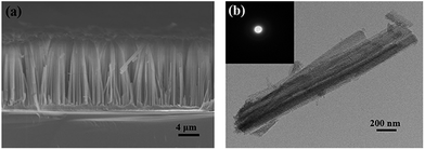
Freshly synthesized Si NWs are distinguishable and almost perpendicular to the p-(100) substrate despite several gathered bundles at the tips with a uniform length of ∼13 μm (Fig. 1a). In general, NW arrays fabricated on Si-(100) substrates by metal-assisted chemical etching possess [100] orientation since the [100] direction is the preferred etching direction. However, gathered bundles may appear at the tips of the Si NWs, making Si NW arrays seem not so much aligned. The possible reason is that strong forces, such as dangling bonds and electrostatic charges on the freshly formed surfaces, lead to the formation of bundles at the tips.34 Based on previous literature,21–23,35 Si NWs obtained from highly doped Si wafers exhibit high porosity while retaining their original crystalline structure. These porous Si NW arrays exhibit strong and broad orange luminescence at room temperature, which can be directly observed with a naked eye upon excitation. It should be noted that there is also a study36 reporting luminescent Si NWs obtained from lightly doped Si wafers. After thermal oxidation, as clearly illustrated in the TEM image (Fig. 1b), the oxidized Si NWs maintain similar rough surfaces and remain porous. Note that their porous morphology seems stable such that it can be maintained even when the NWs are completely oxidized to SiO2 (inset of Fig. 1b). However, the obtained porous SiO2 NWs are almost non-luminescent in the wavelength range between 600 and 800 nm (Fig. S1 in the ESI†).Anomalous luminescent quenching
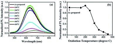
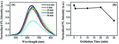
Generally, the porous nature of Si NWs is widely believed11,23 to contribute to their efficient photoluminescence. For instance, Canham et al.11,37 claimed that visible light emission of porous silicon resulted from the quantum confinement effect and had a close relationship with the amorphous phase contained in the porous structures. In addition, during the experimental process, a thin oxide layer is commonly capped on the surface of chemically etched Si NWs. The layer passivates the defects (e.g., the oxide-related centers on the surface of the NWs) and may thus affect emission. As abovementioned, PL of porous Si NWs quench entirely when majority of Si is converted to SiO2. Coincidentally, significant PL quenching also appears in Si NWs oxidized above 500 °C (Fig. S2†), which seems a proper oxidation temperature for Si.27,31 This dramatic PL quenching possibly results from the barrier effect of excessively thick oxide layers.38,39 Therefore, to gain more insight into the quenching effect, mild oxidation condition is considered to be necessary.Thermal oxidation is performed immediately after metal-assisted chemical etching synthesis of Si NWs. Since the surface of Si NWs is H-terminated, oxidation treatment of the freshly prepared Si NWs becomes easier. On the other hand, the porous structure offers large specific surface area, promoting the oxidation process as well. Since the oxide layer can be formed under mild oxidation conditions (Fig. S3†), lower oxidation temperature and shorter oxidation time are used in porous Si NWs for systematic optical studies, and their corresponding PL spectra are displayed in Fig. 2 and 3, respectively. With quite a short oxidation time (1 min), the efficient orange emission around 650 nm maintains its original intensity at low oxidation temperatures until a feeble quenching (∼10%) occurs at 250 °C. After this, PL quenching becomes increasingly obvious as the oxidation temperature increases. With a thicker oxide layer (Fig. S3c†), the emission intensity decreases to 43%, 19%, and 11% of its original value at 300, 350, and 400 °C, respectively, and achieves complete quenching at 450 °C. Moreover, extended oxidation time benefits PL quenching even at a very low oxidation temperature of 250 °C (Fig. 3). The slight PL quenching effect exhibits no obvious difference for the oxidation time within 20 min, whereas a ∼50% sharp decrease occurs in the 30 min-oxidized sample. As a result, in the case of our porous Si NWs, the proper oxidation conditions need to be controlled in the temperature range from 250 to 400 °C as well as within an oxidation time of 30 min.
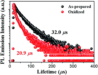
The effect of thermal oxides on the PL properties of porous Si has been studied for a long time. It has been found that PL intensity from p-type porous Si tends to increase with oxidation degree,27,40 whereas porous Si derived from n-type wafers tends to lose its PL intensity. In our experiments, however, we observed quenching of the PL from p-type porous Si NWs after oxidation, contrary to the reported results. The mechanism of the dopant dependency as well as the discrepancy between our results and those reported is not clear to date. To obtain more information, PL lifetime measurements were performed. PL decay spectra of Si NWs before and after thermal oxidation treatment (400 °C, 1 min) are plotted in Fig. 4. Obviously, the PL lifetime shows a slight decrease after oxidation. The curves are fitted by the bi-exponential decay (Fig. S4†):
I(t) = Ar![[thin space (1/6-em)]](https://www.rsc.org/images/entities/char_2009.gif) exp(−t/τr) + Anr exp(−t/τr) + Anr![[thin space (1/6-em)]](https://www.rsc.org/images/entities/char_2009.gif) exp(−t/τnr) exp(−t/τnr)
| (1) |
| τeff = (Arτr2 + Anrτnr2)/(Arτr + Anrτnr) | (2) |
As described in Fig. 4, PL lifetime for porous Si NWs decreases from 32.0 μs to 20.9 μs after thermal oxidation. The weight ratio Anr/Ar obtained from the best fit (yellow line in Fig. S4†) is 2.218 for the original Si NW, whereas it increases to 4.248 after oxidation. Moreover, the nonradiative lifetime τnr decreases from 16.3 to 8.0 μs. Furthermore, similar PL lifetime tendency is observed at all temperatures (Fig. S5†). The results indicate markedly increased recombination rate of nonradiative channels after oxidation, leading to PL quenching.
Enhanced PL stability
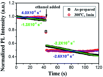
On account of the strong electrochemical reaction during fabrication, porous Si nanostructures are widely accepted to possess various complex surface states and defects. As one of the main viewpoints of the luminescence origin of porous Si, the surface defect model attributes the PL to oxygen-related defect centers at the interface between the Si core and the native oxides or host matrix. Prokes et al.19 claim that the presence of oxygen shallow donors shows distinct correlation with the orange emission intensity observed in porous Si. Moreover, surface states generally result in carrier trapping and/or surface recombination, which are harmful for luminescence efficiency. As a consequence, PL performance of porous Si nanostructures is extremely sensitive to the surface. Indeed, the native hydride surface of porous Si is too reactive to provide a stable PL response in atmospheric or aqueous environments since a variety of molecules have been found to quench photoluminescence from porous Si.41–44 In this case, it is not surprising that porous Si NWs synthesized through metal-assisted chemical etching exhibit low PL stability.Agreeing well with several previous studies,21,45 presence of ethanol results in a loss of PL intensity from porous Si NWs. This PL quenching can occur at very low analyte concentrations: for the as-prepared Si NW sample, its PL intensity decreases to approximately half of the original value even when only a drop of ethanol is added (Fig. 5). Moreover, very interestingly, removal or volatilization of ethanol gives rise to the recovery of PL,21,46 and this reversible effect occurs with almost any nonaqueous liquid at very low vapor concentrations.40 Apart from liquids, detectable PL loss of porous Si NWs takes place in air as well. The emission intensity diminishes upon continuous excitation both before and after the addition of ethanol. PL quenching can be regarded as a linear attenuation, and the slope for the decline line is calculated to be 1.3 × 10⁻³ s−1 in air and 2.2 × 10⁻³ s−1 in ethanol (annotated in Fig. 5 with green color). As clearly shown in Fig. 5, PL stability of porous Si NWs achieves significant improvement after proper thermal oxidation (300 °C, 1 min). The thin oxidation layer passivates the reactive surface of the porous Si NWs and thus stabilizes luminescence. After oxidation, slopes of the decline line, both before and after ethanol addition, become very close to zero (4.0 × 10⁻⁵ and 2.6 × 10⁻⁵ s−1, respectively, as indicated in Fig. 5 with blue color), nearly two orders smaller than the original values.
Note that all Si NWs oxidized at temperatures between 150 and 450 °C present better PL stability in air when compared with the original Si NWs, especially at 400 and 450 °C (shown in Fig. S6†). As for PL stability in ethanol, although not much enhancement is observed in samples oxidized at low temperatures (150 and 200 °C), samples oxidized at higher temperatures (above 250 °C) exhibit obvious enhancement. Therefore, thermal oxidation (above 250 °C) contributes to the enhancement of the PL stability in both air and ethanol. Considering the significant PL quenching at high oxidation temperatures (400 and 450 °C), temperature between 250 and 350 °C is considered as the proper oxidation condition.
From the abovementioned results and discussion, proper thermal oxidation can significantly improve the PL stability of porous Si NWs in both air and ethanol. We believe that the remarkable enhancement in PL stability may provide a simple processing approach for their high-performance applications, especially in the field of PL sensing.
Conclusions
In summary, a systematic PL study is presented on oxidized porous Si NWs obtained under various thermal oxidation conditions. The oxidized Si NWs maintain a rough surface and porosity even when they are completely oxidized to SiO2. By contrast, the efficient orange emission of the original porous Si NWs can be easily quenched with a very low ultimate oxidation temperature of 250 °C within a short oxidation time of 20 min. These thermal oxidation parameters are much milder than those in most of the reported studies on porous Si. Furthermore, proper thermal oxidation (e.g., 300 °C, 1 min) can significantly improve PL stability in both air and ethanol, providing a simple processing approach for their high-performance applications (e.g., PL sensing). Both luminescence quenching behaviour and remarkably improved PL stability in this mildly oxidized porous Si NWs may open new opportunities in the field of semiconductor optical applications.Acknowledgements
This work was financially supported by the Natural Science Foundation of China under Grant No. 51372223.Notes and references
- S. N. Raja, R. Rhyner, K. Vuttivorakulchai, M. Luisier and D. Poulikakos, Nano Lett., 2017, 17, 276–283 CrossRef PubMed.
- P. H. Xue, J. J. Nan, T. Q. Wang, S. L. Wang, S. S. Ye, J. H. Zhang, Z. C. Cui and B. Yang, Small, 2017, 13, 1601807 CrossRef PubMed.
- S. Xu, Z. Yan, K. I. Jang, W. Huang, H. R. Fu, J. Kim, Z. Wei, M. Flavin, J. McCracken, R. Wang, A. Badea, Y. Liu, D. Q. Xiao, G. Y. Zhou, J. Lee, H. U. Chung, H. Y. Cheng, W. Ren, A. Banks, X. L. Li, U. Paik, R. G. Nuzzo, Y. G. Huang, Y. H. Zhang and J. A. Rogers, Science, 2015, 347, 154–159 CrossRef CAS PubMed.
- M. Amato and R. Rurali, Prog. Surf. Sci., 2016, 91, 1–28 CrossRef CAS.
- M. A. Rahman, G. S. Song, A. I. Bhatt, Y. C. Wong and C. E. Wen, Adv. Funct. Mater., 2016, 26, 647–678 CrossRef CAS.
- X. Cartoixa, R. Dettori, C. Melis, L. Colombo and R. Rurali, Appl. Phys. Lett., 2016, 109, 013107 CrossRef.
- Y. W. Jiang, J. L. Carvalho-de-Souza, R. C. S. Wong, Z. Q. Luo, D. Isheim, X. B. Zuo, A. W. Nicholls, I. W. Jung, J. P. Yue, D. J. Liu, Y. C. Wang, V. De Andrade, X. H. Xiao, L. Navrazhnykh, D. E. Weiss, X. Y. Wu, D. N. Seidman, F. Bezanilla and B. Z. Tian, Nat. Mater., 2016, 15, 1023–1030 CrossRef CAS PubMed.
- J. A. Perez-Taborda, M. M. Rojo, J. Maiz, N. Neophytou and M. Martin-Gonzalez, Sci. Rep., 2016, 6, 32778 CrossRef CAS PubMed.
- E. Tolstik, L. A. Osminkina, C. Matthaus, M. Burkhardt, K. E. Tsurikov, U. A. Natashina, V. Y. Timoshenko, R. Heintzmann, J. Popp and V. Sivakov, Nanomedicine: Nanotechnology, Biology and Medicine, 2016, 12, 1931–1940 CrossRef CAS PubMed.
- L. D. Lin, X. N. Xu, C. X. Chu, M. K. Majeed and J. Yang, Angew. Chem., Int. Ed., 2016, 55, 14063–14066 CrossRef CAS PubMed.
- L. T. Canham, Appl. Phys. Lett., 1990, 57, 1046–1048 CrossRef CAS.
- L. T. Canham, W. Y. Leong, M. I. J. Beale, T. I. Cox and L. Taylor, Appl. Phys. Lett., 1992, 61, 2563–2565 CrossRef CAS.
- I. Leontis, M. A. Botzakaki, S. N. Georga and A. G. Nassiopoulou, J. Appl. Phys., 2016, 119, 244508 CrossRef.
- S. H. Lee, J. W. Kim, T. I. Lee and J. M. Myoung, Small, 2016, 12, 4222–4228 CrossRef CAS PubMed.
- K. Peng, A. Lu, R. Zhang and S.-T. Lee, Adv. Funct. Mater., 2008, 18, 3026–3035 CrossRef CAS.
- H. A. Chen, H. Wang, X. H. Zhang, C. S. Lee and S. T. Lee, Nano Lett., 2010, 10, 864–868 CrossRef CAS PubMed.
- C.-Y. Chen, C.-S. Wu, C.-J. Chou and T.-J. Yen, Adv. Mater., 2008, 20, 3811–3815 CrossRef CAS.
- Q. Q. Yu, H. P. He, L. Gan and Z. Z. Ye, RSC Adv., 2015, 5, 80526–80529 RSC.
- S. M. Prokes, W. E. Carlos and O. J. Glembocki, Phys. Rev. B: Condens. Matter Mater. Phys., 1994, 50, 17093–17096 CrossRef CAS.
- J. W. Wang, H. Luo, Y. Liu, Y. He, F. F. Fan, Z. Zhang, S. X. Mao, C. M. Wang and T. Zhu, Nano Lett., 2016, 16, 5815–5822 CrossRef CAS PubMed.
- L. Gan, H. He, L. Sun and Z. Ye, Phys. Chem. Chem. Phys., 2014, 16, 890–894 RSC.
- L. Gan, L. W. Sun, H. P. He and Z. Z. Ye, J. Mater. Chem. C, 2014, 2, 2668–2673 RSC.
- H. He, C. Liu, L. Sun and Z. Ye, Appl. Phys. Lett., 2011, 99, 123106 CrossRef.
- T. Nikitin and L. Khriachtchev, Nanomaterials, 2015, 5, 614–655 CrossRef CAS PubMed.
- A. Ilyas, N. V. Lavrik, H. K. W. Kim, P. B. Aswath and V. G. Varanasi, ACS Appl. Mater. Interfaces, 2015, 7, 15368–15379 CAS.
- L. Cui, W. W. Xia, F. Wang, L. J. Yang and Y. J. Hu, Physica B, 2013, 409, 47–50 CrossRef CAS.
- L. J. Liu and T. K. Sham, Small, 2012, 8, 2371–2380 CrossRef CAS PubMed.
- J. M. Bae, W. J. Lee, J. W. Ma, J. H. Kim, S. H. Oh, M. H. Cho, K. Chul, S. Jung and J. Park, J. Mater. Chem. C, 2015, 3, 2123–2131 RSC.
- N. Fukata, T. Oshima, N. Okada, K. Murakami, T. Kizuka, T. Tsurui and S. Ito, J. Appl. Phys., 2006, 100, 024311 CrossRef.
- N. Fukata, T. Oshima, K. Murakami, T. Kizuka, T. Tsurui and S. Ito, Appl. Phys. Lett., 2005, 86, 213112 CrossRef.
- N. Fukata, S. Ishida, S. Yokono, R. Takiguchi, J. Chen, T. Sekiguchi and K. Murakami, Nano Lett., 2011, 11, 651–656 CrossRef CAS PubMed.
- T. K. Sham, S. J. Naftel, P. S. G. Kim, R. Sammynaiken, Y. H. Tang, I. Coulthard, A. Moewes, J. W. Freeland, Y. F. Hu and S. T. Lee, Phys. Rev. B: Condens. Matter Mater. Phys., 2004, 70, 045313 CrossRef.
- L. S. Liao, X. M. Bao, X. Q. Zheng, N. S. Li and N. B. Min, Appl. Phys. Lett., 1996, 68, 850–852 CrossRef CAS.
- M. L. Zhang, K. Q. Peng, X. Fan, J. S. Jie, R. Q. Zhang, S. T. Lee and N. B. Wong, J. Phys. Chem. C, 2008, 112, 4444–4450 CAS.
- Y. Q. Qu, L. Liao, Y. J. Li, H. Zhang, Y. Huang and X. F. Duan, Nano Lett., 2009, 9, 4539–4543 CrossRef CAS PubMed.
- H. H. Chen, R. J. Zou, H. H. Chen and J. Q. Hu, J. Mater. Chem., 2011, 21, 801–805 RSC.
- A. G. Cullis and L. T. Canham, Nature, 1991, 353, 335–338 CrossRef CAS.
- W. Lang, P. Steiner, F. Kozlowski and P. Ramm, Thin Solid Films, 1995, 255, 224–227 CrossRef CAS.
- J. Lopez-Vidrier, Y. Berencen, S. Hernandez, B. Mundet, S. Gutsch, J. Laube, D. Hiller, P. Loper, M. Schnabel, S. Janz, M. Zacharias and B. Garrido, Nanotechnology, 2015, 26, 185704 CrossRef CAS PubMed.
- M. J. Sailor and E. C. Wu, Adv. Funct. Mater., 2009, 19, 3195–3208 CrossRef CAS.
- M. C. Ko and G. J. Meyer, Chem. Mater., 1995, 7, 12–14 CrossRef CAS.
- D. L. Fisher, J. Harper and M. J. Sailor, J. Am. Chem. Soc., 1995, 117, 7846–7847 CrossRef CAS.
- S. Content, W. C. Trogler and M. J. Sailor, Chem.–Eur. J., 2000, 6, 2205–2213 CrossRef CAS.
- J. H. Song and M. J. Sailor, J. Am. Chem. Soc., 1997, 119, 7381–7385 CrossRef CAS.
- J. Dian, V. Vrkoslav and I. Jelinek, Sens. Actuators, B, 2010, 147, 406–410 CrossRef CAS.
- J. M. Lauerhaas, G. M. Credo, J. L. Heinrich and M. J. Sailor, J. Am. Chem. Soc., 1992, 114, 1911–1912 CrossRef CAS.
Footnote |
| † Electronic supplementary information (ESI) available: Fig. S1–S6. See DOI: 10.1039/c7ra05012g |
| This journal is © The Royal Society of Chemistry 2017 |

