
 Open Access Article
 This Open Access Article is licensed under a
 Creative Commons Attribution 3.0 Unported Licence
Formation of large-area stretchable 3D graphene–nickel particle foams and their sensor applications
Cheng Yang†
 a,
Yuanyuan Xu†a,
Peihong Manb,
Hao Zhanga,
Yanyan Huoa,
Chuanxi Yangc,
Zhen Lia,
Shouzhen Jiangad and
Baoyuan Man*ad
a,
Yuanyuan Xu†a,
Peihong Manb,
Hao Zhanga,
Yanyan Huoa,
Chuanxi Yangc,
Zhen Lia,
Shouzhen Jiangad and
Baoyuan Man*ad
aSchool of Physics and Electronics, Shandong Normal University, Jinan 250014, People's Republic of China. E-mail: byman@sdnu.edu.cn
bMicrophysics Laboratory, Department of Physics, University of Illinois at Chicago, Chicago, IL 60607-7059, USA
cChina Agricultural University, Beijing 100083, People's Republic of China
dInstitute of Materials and Clean Energy, Shandong Normal University, Jinan 250014, People's Republic of China
First published on 12th July 2017
Abstract
Stretchable sensors are essential and important for the new-type stretchable intelligent electronic devices. Three-dimensional (3D) graphene foams are attractive to increase the sensitivity and stretchability, benefiting from a high specific surface area and mechanical strength. Herein, 3D graphene/nickel particles (Gr–NiP) peasecod foams, which were fabricated using CVD and stamp-transfer processes, are proposed and used for stretchable sensor applications. The existing nickel particles, covered by graphene layers, are useful for the formation of 3D nanostructures and separated from each other for stretchable applications. A stretchability (ε) of such Gr–NiP foams of up to 80% can be achieved. A low limit of detection (<1%) and excellent linearity (R2 = 0.997) are also present. Sunken ravines between the Ni particles provide favorable sites to grow Ag nanoflowers (AgNFs), which can enhance the electromagnetic coupling for SERS application. Such stretchable substrates can be used as ultrasensitive biosensors to detect the molecules on the surfaces of any shape.
1. Introduction
As new equipment, stretchable devices show good properties under greater and long-time mechanical stress conditions, which can be useful for use in human implantation devices, flexible portable devices, and wearable and wireless sensing devices. Stretchable sensors are essential components of the new-type stretchable intelligent electronic devices,1–9 such as the wearable health-monitoring patch,5,6 robotic sensory skin,7,8 and tele-surgery electronic glove.9 Stretchability10 and sensitivity are the primary elements of the stretchable sensors. Existing stretchable sensors based on bulky technologies involving metal and semiconductors11,12 are cheap but have a very limited stretchability. High stretchability (ε > 50%) is of compelling interest for emerging applications, such as human-friendly interactive electronics. For example, the movements of human joints can generate strains as high as 55% upon stretching and contracting.Recently, nanoscale materials have been studied to fabricate stretchable devices. Carbonaceous materials, including carbon nanotubes (CNTs)13–17 and graphene,9,18–26 have drawn tremendous attention due to their advantages of flexibility, fast response, and high sensitivity. Compared with CNTs, graphene-based materials offer a better solution for preparing highly sensitive and stretchable sensors, benefiting from their plane periodic lattice structure, which can be used as an ideal surface support. Piezoresistive monolayer and few-layer graphene have been used for strain detection27–31 with a limited stretchability (<6%).29 Flexible and foldable graphene can also be wrinkled or rippled to produce 3D graphene films to prepare large-area stretchable graphene.18,19
In order to further increase the sensitivity and conductivity of graphene-based sensors, 3D sponge-like graphene foam, which has a rich porous structure with a higher conductivity, specific surface area, and mechanical strength, has been reported.32 3D graphene foams have been fabricated by growing graphene on copper or nickel foam substrate and then etching away the metal template. Such 3D graphene foam, which could be stretched to >100%, is attractive for stretchable devices and consequently has been studied by several researchers.23,32,33
The porous nature of this 3D graphene foam, with a large specific surface area (up to 850 m2 g−1), is also suitable to make functional composites by filling the pores with nanoparticles, polymers, or other functional materials.33 In this study, 3D Gr–NiP nanostructures, composed of graphene and Ni particles, were proposed to fabricate stretchable sensors with a stretchability of 80%. The existing nickel particles, separated from each other and covered by graphene layers, are useful for the creation of 3D nanostructures by preventing a collapse of all the graphene foam onto the stretchable elastomer. A simple stamp-transfer process can be used to transfer such floating Gr–NiP foams.
Sunken ravines between the Ni particles are also can be formed due to the etching processes and the presence of the Ni particles. This gives the possibility of both high stretchability and the favorable sites for the formation of 3D AgNFs by the use of in situ growth methods without any acute conditions (detailed in the methods section). This innovative method puts forward a new idea for the synthesis of 3D nanostructures. Such 3D metal nanostructures (nanospheres,34 nanostars,35 and nanoflowers36), which contain a special fine structure, large specific surface area, and larger size, can avoid the aggregation of the particles during application as SERS.26,34–36
The graphene base can effectively enhance the Raman signal and reduce the back action noise to allow the use as a graphene-SERS based biosensor.20,21,26 There are two key advantages of this system: (1) graphene is a favorable atomic surface test bed with a small-distance charge transfer between the graphene surface and the adsorbed molecules, which makes the Raman signal more reliable and efficient;20 (2) graphene with a large specific surface area of 2630 m2 g−1 can also work as a molecule enricher in SERS-active substrates, which can act as excellent adsorbents toward organic molecules, particularly aromatic molecules.21
It is also well known that more efficient SERS effects can be yielded by 3D SERS substrates compared with planar substrates. The larger surface area improves the target molecule adsorption and pathway for light propagation. Denser “hot spots” can also be obtained by fabrication of 3D metal nanostructures, which are attractive areas for researchers recently. Jones reported that the SERS enhancement factor for 3D “hot spot”-based substrates is more than two orders of magnitude greater than that for two-dimensional (2D) substrates.26 Ultrasensitive SERS performance in 3D “sunflower-like” nanoarrays decorated with Ag nanoparticles36 was also reported by Zhang et al. In our experiment, the obtained 3D AgNFs on graphene foams were used as SERS “hot spots” to improve the sensitivity of the stretchable biosensors.
2. Results and discussion
The three main stages (G/Ni foam formation, flexible Gr–NiP foam formation, stamp-transfer process) to form the stretchable Gr–NiP foam are illustrated in Fig. 1. Chemical vapor deposition (CVD) was used to precipitate carbon atoms on the nickel foam to fabricate the G/Ni foam at 1050 °C. An FeCl3 and HF mixed solution was used to etch different amounts of metal nickel away by adjusting the immersion time to form the flexible Gr–NiP foam. Stamp-transfer, a simple, convenient, and highly efficient method, is proposed here to transfer such a Gr–NiP foam onto the elastomer substrate. After natural drying, the flexible and stretchable Gr–NiP foam, comprising a continuous and interconnected graphene 3D network wrapped around Ni nanoparticles, was obtained.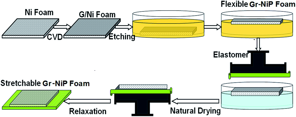 | ||
| Fig. 1 Schematic of the stretchable Gr–NiP foam fabrication. | ||
Graphene layers, which are controlled by the growth time of the CVD deposition, are crucial for the formation of flexible Gr–NiP peasecod foams. When the number of graphene layers is less than three (growth time was shortened than 15 min), all of the metal nickel materials are easily etched away, and the resulting as-prepared graphene foam is so thin and light that it collapses and is suspended in the FeCl3 and HF mixed solution. The suspended graphene foam cannot be transferred by our proposed stamp-transfer processes due to the fact that the elastomer film cannot touch the suspended materials. On the other hand, when the number of graphene layers is more than 15 (growth time extended to 90 min), the obtained graphene foam is over-thick to prevent the intimal metallic Ni from dissolving, and hence the formed Gr–NiP foam is rigid, even though long-time etching has been carried out, which makes it unsuitable for flexible and stretchable devices. In our experiment, stretchable Gr–NiP foam could be formed with 6 to 10-layered graphene (shown in Fig. 2), obtained by 45 min CVD deposition.
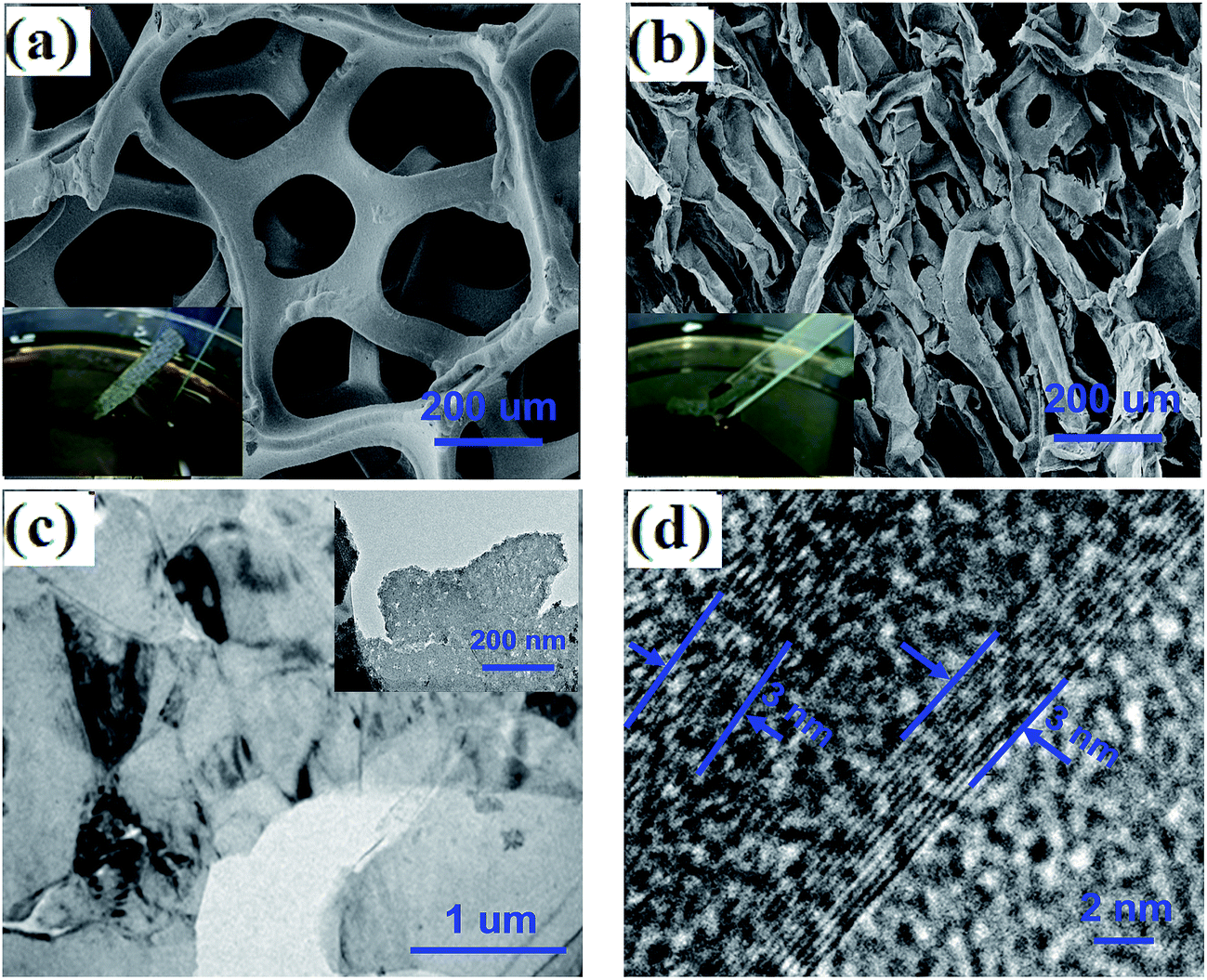 | ||
| Fig. 2 SEM images of G/Ni foam (a) and Gr–NiP foam (b) with 45 min etching (inset is the photo of the corresponding G/Ni foam and Gr–NiP foam samples). (c) TEM image of Gr–NiP foams (inset: the TEM image at a higher magnification). (d) HRTEM image of the 10-layered graphene. | ||
The stamp-transfer method (shown in Fig. 1), which is appropriate for flexible, light, flimsy, and gummy elastomer substrates, is innovatively suggested here. The gummy elastomer substrate (3M4910 VHB), which was affixed to the edge of a plastic culture dish, is coated quickly and horizontally onto the floating flexible Gr–NiP foam for 10 s and then uplifted slowly at an oblique angle. By virtue of this transfer method, the as-prepared flexible Gr–NiP foam was attached on the elastomer substrates by the gummy of the elastomer and by the van der Waals interactions of Gr–NiP and the elastomer. Essentially, the stamp-transfer processes can also be used on other substrates (such as Si wafer, glass) without viscidity.
It is critical to investigate the morphology and crystallization of the Gr–NiP foam for understanding its electrical and mechanical properties. Scanning electron microscopy (SEM, Zeiss Gemini Ultra-55) was used for the morphology characterization of such a Gr–NiP foam. Compared to that of the G/Ni foam (Fig. 2a), the graphene skeleton of the Gr–NiP foam (Fig. 2b) was oblate and the space between the layers decreased drastically. The frame structure of the foam possesses an irregular rectangle structure instead of the hexagonal structure, and a surface structure with more ridges was detected on the stretchable Gr–NiP foam. These ridges surfaces and shape changes of the frame structure, combined with the self-constricted structures, make the Gr–NiP foam suitable for flexible and stretchable sensors. Moreover, the fabricated Gr–NiP foam still maintains a monolith of a 3D network, providing a channel for charge carriers to move rapidly through the high-quality and continuous building blocks with low resistance. Therefore, extraordinary electrical and mechanical properties of Gr–NiP foam were expected.
Because the graphene layers were synthesized on the surface of the metallic Ni, most of the Ni particles are covered by the graphene layer. The TEM images of the obtained Gr–NiP foams are presented in Fig. 2c and d, which prove the existence of multilayer graphene (3 nm, ∼10 layers) and Ni nanoparticles. As shown in Fig. 2c, the black areas represent the Ni particles aggregation bodies, which are covered by the graphene layers. The inset exhibits the TEM image under high magnification, in which there are still a mass of Ni particles scattered in the relative gray areas.
To investigate the electromechanical response of such a Gr–NiP foam, both ends of the as-prepared stretchable Gr–NiP foam were immobilized on a motorized moving controller, as shown in Fig. 3. Different strain/release cycles were carried out by virtue of the different strain levels and frequencies, while the resistance changes were measured using a Keithley 4200 device. Owing to the strong adhesive strength of the gummy acrylic acid substrates, the adhesion between the foams and the substrate was very strong, and the graphene foams follow the deformation of the stretched acrylic acid substrate.37 When the elastomer film was uniaxially or biaxially stretched and relaxed over multiple cycles (more than 1000 cycles in our experiment), the Gr–NiP foam still maintained its integrity and a perfect electromechanical performance, which can be attributed to its flexibility and high fracture toughness.
 | ||
| Fig. 3 Photographs of the strain sensor before (a) and after stretching of (b) ε = 50%, (c) ε = 100%, (d) ε = 150%. | ||
In order to investigate the influence of the size and number of Ni particles on the electrical resistance response of the Gr–NiP-based sensors, typical curves of the normalized resistance changes as a function of applied strain for the Gr–NiP-based sensors with different Ni element densities controlled by different etching time were obtained and are shown in Fig. 4. The normalized relative resistances of the Gr–NiP-based sensors all increased upon the application of strain. The change in the electrical conductance is the main reason for the Gr–NiP foam-based sensor to act as a type of resistance-strain sensor. Upon stretching, the graphene foam was elongated, such that some Ni particles may become separated within the graphene foam, which represents the reason for the electrical conductance reduction.38,39 Interestingly, the sensitivity, linearity, and stretchability of the strain sensors could be tuned by adjusting the etching time of the G/Ni foam.
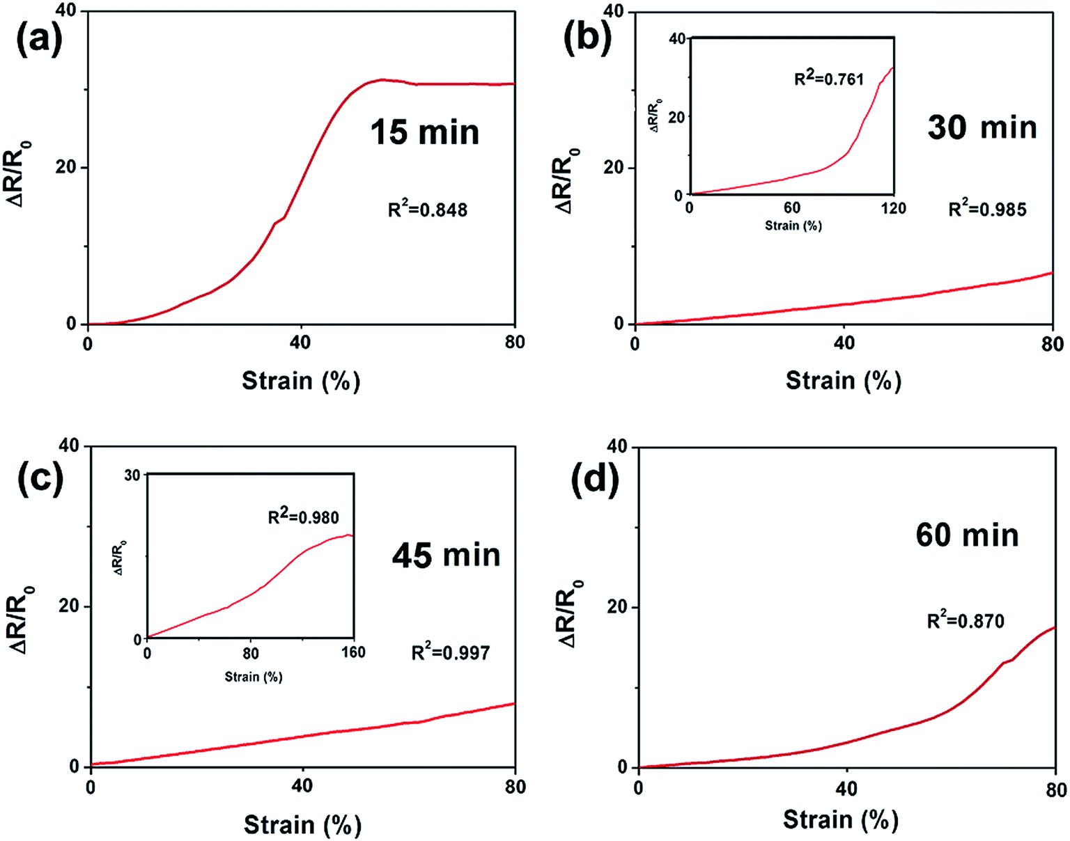 | ||
| Fig. 4 Typical curves of the normalized resistance changes as a function of applied strain for the Gr–NiP-based sensors with different Ni element densities controlled by different etching times: (a) 15 min, (b) 30 min, (c) 45 min, (d) 60 min. | ||
Due to the gradual reduction of embedded Ni metal and the surface roughness of the gummy acrylic acid substrates, the stretchability of Gr–NiP increased gradually with an increase in the etching time. Fig. 4a shows the normalized relative resistance changes of Gr–NiP foams for 15 min etching time under different applied strains. Because relatively more Ni particles existed in the Gr–NiP foam undergoing 15 min etching, a failure strain of <50% and a relatively weak linearity (R2) of 0.848 were obtained. When the etching time was increased from 15 min to 30 min, as shown in Fig. 4b and the inset of Fig. 4b, it exhibited excellent linear electromechanical performance in 0–80%, and a stretchability (ε) of up to 120% was achieved. Moreover, in the stretchability range of 80–120%, the Gr–NiP peasecod foam-based strain sensors still showed an excellent linear performance. As a demarcation point, when the foam substrate was stretched beyond 80%, the Gr–NiP peasecod foams transform from “homogeneous foam” to “inhomogeneous foam” with emerging bottleneck locations that critically limited the electrical current, which led to serious nonlinearity in the entire stretchability range.
The limit of detection (LOD) of strain sensors is important to the development of effective ultra-low and subtle-strain sensors. A low LOD means that a subtle applied strain is able to arouse large normalized resistance change. With the etching time further increasing from 30 min to 45 min, as shown in Fig. 4c, Gr–NiP foams with a very low limit of detection were also present and the strain sensors responded to the applied strain with excellent linearity (R2 = 0.997) for the range from 0% to 80%. Amazingly, as shown in the inset of Fig. 4c, the Gr–NiP foams showed outstanding stretchability, which increased from 120% to 160%, showing a 40% improvement. In particular, in a quite wide range of strains (from 0% to 160%), the linearity of the strain sensors just showed a negligible change, decreasing from 0.997 to 0.980.
As can be seen in Fig. 4d, when the etching time was further increased from 45 min to 60 min, because all or almost all the Ni skeleton was etched away, which leads to collapse of the 3D foam structure, the stretchability and linearity of the sample all declined.
The sensing ability of Gr–NiP foam was further investigated and is shown in Fig. 5. Fig. 5a depicts the relative resistance responses of stretching-releasing cycles of Gr–NiP foams undergoing 45 min etching under various applied strains. In the multiple stretching–releasing cycles loaded with different strains, the response signal still remained at a stable performance despite the return occurring in the stretching processes under large tensile stress loading. In addition, the recoverability of the Gr–NiP-based strain sensors was investigated. As shown in Fig. 5b, the stretching and releasing curves showed nearly reversible behavior, and hysteresis was negligible. Negligible hysteresis at lower applied strains (ε ≤ 10%) arises from strong interfacial binding between nanomaterials and elastic polymers.40–46
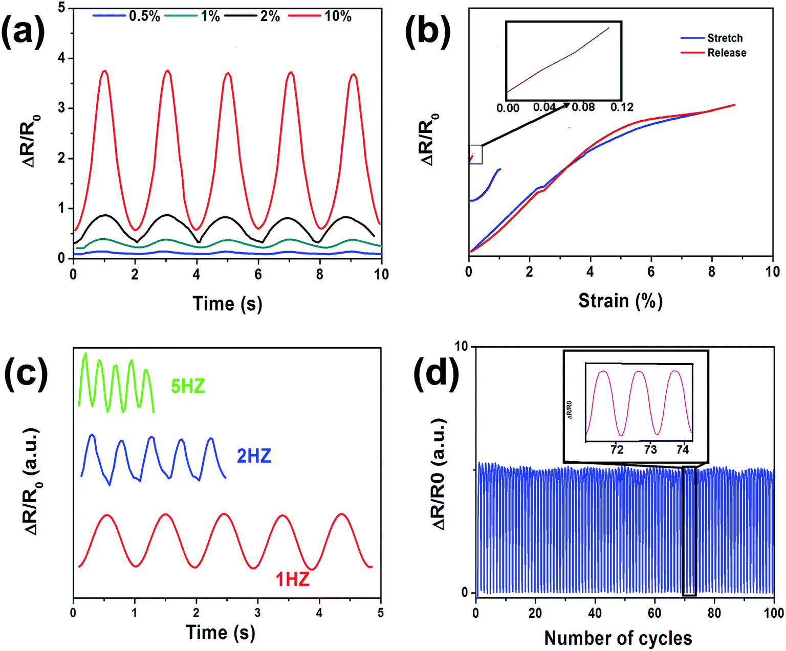 | ||
| Fig. 5 (a) Relative resistance response of Gr–NiP foams as a function of time (strain frequency: 0.5 Hz) for different applied strains (0.5%, 1%, 2%, and 10%). (b) Reversible stretch-release behavior for Gr–NiP foams under the frequency of 0.5 Hz. (c) Relative resistance responses of Gr–NiP foams at different frequencies under 50% strain. (d) Cyclic test for a low strain level (ε = 10%). | ||
Durability and stability are extremely critical for the practical application of strain sensors. Electrical responses of the strain sensors based on Gr–NiP foams exhibited good stability with 50% strain at frequencies ranging from 1 to 5 Hz (Fig. 5c). The variations of the relative resistance signals were almost the same as the increase in frequency. The response of the strain sensors to cyclic loading from 0 to 10% strain for more than 100 cycles with good stability and reproducibility is illustrated in Fig. 5d, which could be attributed to strong adhesion between Gr–NiP foams and acrylic acid substrates.
Applications of the graphene-based biosensor (such as G-SERS) have drawn a tremendous amount of attention recently due to their flexibility, chemical absorption, and the reduction of the back action noise.47,48 To improve the performance of graphene toward high sensitive SERS applications, recent studies have focused on the hybrid nanostructures combined with metal nanostructure.48,49 Herein, we found that 3D AgNFs could be easily synthesized on such Gr–NiP foam to use as a stretchable graphene-SERS based biosensor.
The as-prepared AgNFs, synthesized under the molar ratio of ascorbic acid (AA) to Ag+ of 0.5, were large scale and uniform with spherical structures in a high yield (shown in Fig. 6a). Such closely arranged AgNFs were quasi-spherical, consisting of a solid core with a large amount of small, ellipsoidal surface protuberances. The average overall dimension of these quasi-spherical AgNFs was 200 nm, and the surface protuberances were quasi-ellipsoids with a variety of sizes. These AgNFs possessed highly roughened surfaces due to the considerable inhomogeneity, with nanoscale ravines on the surfaces of the crystals and a wide variety of ravines on different AgNFs.
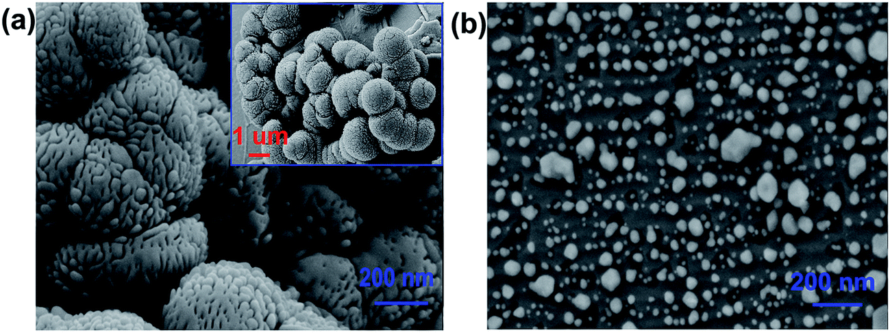 | ||
| Fig. 6 (a) SEM image of AgNFs grown on Gr–NiP foam substrates. (b) SEM image of silver nanoparticles grown on G/Ni foam substrates without etching. Inset of (a) shows image of AgNFs grown on the sunken ravines between the Ni particles. | ||
In contrast, Ag nanoparticles (AgNPs) were obtained on the unabridged G/Ni foam substrates without the etching process (Fig. 6b). We believe that the basal surface topography has a big effect on the pattern of Ag nanostructures. Unlike G/Ni foam substrates with a smooth graphene skeleton, due to the etching of the Ni skeleton, the skeleton of Gr–NiP foam substrates appeared to collapse to some extent, causing numerous wrinkles, imperfections, and edges. Moreover, adjacent skeleton layers are closer and even stick together, which provide favorable sites for the deposition and aggregation of Sn+. After silver seed deposition, a large number of primary irregular Ag nanoparticles were instantaneously formed on the sunken ravines between the Ni particles (as shown in the inset of Fig. 6a). After the samples were immersed in the mixed solution of AgNO3 and ascorbic acid for the further growth, the as-formed structures began to act as the sites for further Ag precipitation. Following a 3D-oriented attachment,45 irregular Ag particles grew and transformed into rough surface nanoflowers after a period of treatment.
The presence of such aggregates of Ag ellipsoids is expected to significantly promote local field enhancements on the surface of these roughened AgNFs, which might be used as the perfect “hot spots” to enhance their SERS efficiency. R6G molecules were applied as probe molecules to evaluate the SERS sensitivity and reproducibility of the AgNF-decorated Gr–NiP foams as SERS substrates. Fig. 7a represents the SERS spectra of R6G with the concentration varying from 10−6 to 10−11 M. The characteristic signals of R6G still can be clearly resolved even at 10−11 M, which indicates the potential for sensitive and fast detection. Moreover, to show the capability of quantitative detection, the SERS intensity of the vibration located at 613, 778, and 1365 cm−1 versus the concentration (10−6 to 10−9) of R6G as well as the linear fit calibration curves of these three characteristic peaks is plotted in Fig. 7b. The coefficient of determination (R2) of the linear fit calibration curve for the peaks of 613, 778, and 1365 cm−1 reached to 0.971, 0.902, and 0.905, respectively. The intensities of the SERS spectra of R6G are proportional to the logarithm of the concentrations of the R6G. The good line correlation indicates a great potential application of such a stretchable foam to detect analytes in real biological systems. Fig. 7c exhibits the SERS spectra of 10−6 M R6G adsorbed on the four randomly chosen AgNFs aggregates. The detected Raman peaks show similar SERS responses, which indicate a high reproducibility.50–54
 | ||
| Fig. 7 (a) Raman spectra of R6G molecules on AgNF-decorated Gr–NiP foams with different concentrations from 10−6 to 10−11 M. (b) Raman intensity of R6G peaks at 613, 778, and 1365 cm−1 as a function of the R6G molecular concentration with the high coefficient of determination (R2) of 0.971, 0.902, and 0.905, respectively. (c) SERS spectra were collected from 4 randomly selected AgNFs aggregates from the Gr–NiP peasecod foam. (d) Raman spectra of R6G molecules on AgNF-decorated Gr–NiP foams in the state of stretching. | ||
The hybrid substrate exhibited excellent SERS properties and malleability, which could be bent back and forth without any breakdown. To demonstrate the wide suitability of SERS substrates under different states, such as tension and bending, we further studied the SERS performance of AgNF-decorated Gr–NiP foam in the state of stretching by applying different stretching forces to it. Fig. 7d shows the SERS performance of such substrates under stretching. The SERS performance was consistent when undergoing different deformation, indicating that such substrates can be used as cut-and-paste SERS substrates to cover the surface of arbitrary configurations for highly sensitive in situ detection.
To further investigate the practical application of the AgNF-decorated Gr–NiP foams as stretchable biosensors, a type of food additive was examined. Methylene blue (MB), an aromatic heterocyclic compound, is often illegally added into water bodies to increase the fish livability in the process of fish breeding by some vendors.52 Fish tiddlers were immersed in the new-prepared MB solution with different concentrations from 0.01 mM to 10 nM for half an hour and then covered by the stretchable AgNF-decorated Gr–NiP substrate to directly absorb MB solution from the fish surface. The collected SERS spectra of MB are demonstrated in Fig. 8a. Several vibrational peaks located at about 449, 505, 678, 1036, 1072, 1387, 1440 and 1622 cm−1 can be observed, which belong to MB according to the normal Raman spectrum of MB powder. The lowest detected concentration of MB was 10 nM in our experiment. This fact indicates that the stretchable biosensor possessed excellent adsorption abilities and SERS properties. To prove the capability of the stretchable substrate products in the quantitative detection of MB, the linear fit calibration curve is illustrated in Fig. 8b. The intensities of the SERS spectra of MB at 678 and 1440 cm−1 are proportional to the logarithm of the concentrations of the MB with a good linear relationship (R2 = 0.9, 0.88 respectively) ranging from 0.01 mM to 10 nM.
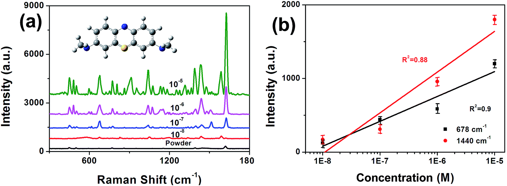 | ||
| Fig. 8 (a) Raman spectra of MB molecules collected by AgNF-decorated Gr–NiP foam from the fish surface with different concentrations from 10−5 to 10−8 M. (b) Raman intensity of MB peaks at 678 and 1440 cm−1 as a function of the MB molecular concentration, respectively. | ||
COMSOL simulation based on such AgNFs and Ag hemispheres is shown in Fig. 9, where the size of the AgNFs was settled according to the actual shape, as shown in Fig. 6. The electromagnetic enhancement (EM) is well known as the main mechanism of SERS for metallic nanostructures (such as AgNPs).55 Local surface plasmon resonances (LSPRs) existing in the gaps between the metal particles enhance the local electric field near the metallic nanostructure significantly, which produces an enhancement highly localized to the metal surface. Fig. 9a and b show the y–z views of the electric field distribution on the AgNFs and Ag hemisphere by a plane wave of 532 nm. It can be seen clearly that, compared with that of a smooth Ag hemisphere, more and denser hotspots are widely spread across the surface of AgNFs, and the local electric field of the incident light is magnified strongly. Fig. 9c–f show the x–y views of the electric field distribution on the AgNFs at different heights (h = 0, 90, 100, 110 nm), respectively. A large number of strong and high-density hotspots are scattered across the entire surface of the AgNFs, which is well consistent with the SERS experimental results. Based on the theoretical results, the 3D AgNF-decorated Gr–NiP substrate is a truly outstanding candidate for a higher sensitivity stretchable SERS substrate.
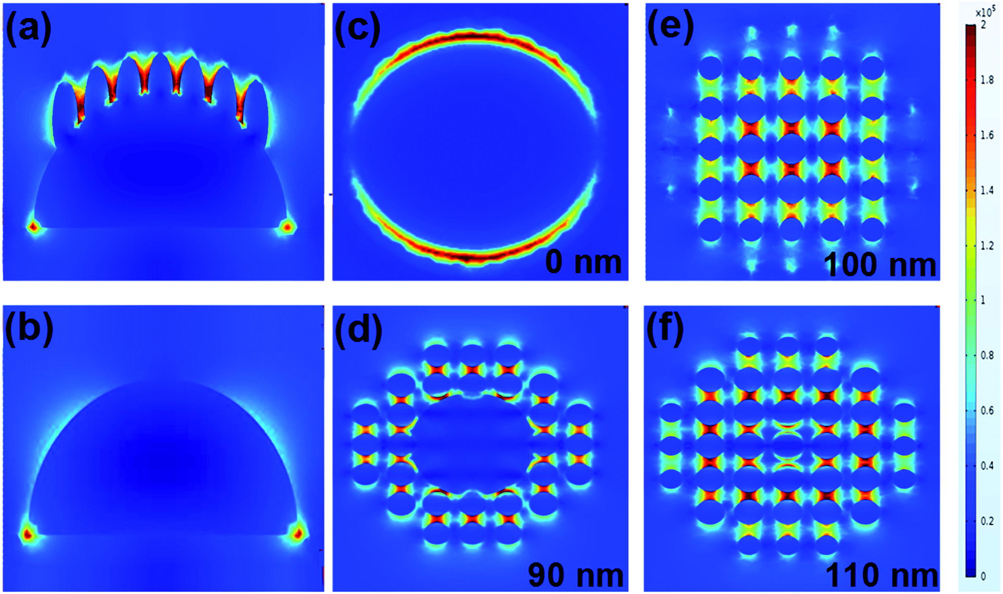 | ||
| Fig. 9 (a) and (b) are respectively the y–z views of the electric field distribution on the AgNFs and Ag hemisphere. (c)–(f) are respectively the y–x views of different heights (h = 0, 90, 100, 110 nm) of the electric field distribution on the AgNFs. | ||
3. Conclusion
Novel and high-performance stretchable sensors based on the new 3D Gr–NiP are proposed by virtue of an imaginative stamp-transfer process. By controlling the thickness of the graphene layers and by optimizing the etching time, such a strain sensor exhibited perfect sensitivity, stretchability, a low limit of detection, and excellent linearity. AgNFs, profiting from the sunken ravines, could be easily synthesized on such a Gr–NiP substrate to form a stretchable SERS substrate. The combined advantages of electromagnetic enhancement from the AgNFs and the chemical absorption of graphene could be used to obtain an ultrasensitive biosensor to detect molecules on the surfaces of any shape.4. Experimental
Flexible Gr–NiP peasecod foam formation
To fabricate the G/Ni foam, a scaffold of porous nickel foam was used as a template for the deposition of carbon atoms. The large-area multilayer graphene was grown by CVD technology as described in previous work.27–29 Briefly, after the pressure of a quartz tube was pumped to under 10−3 Pa by a double-pump system, H2 with the flow of 50 sccm was piped into the tube to remove the remaining nickel oxide when the temperature reached 300 °C. The growth process of graphene was carried out at 1050 °C with a mixed flow of H2 (50 sccm) and CH4 (50 sccm). The nickel scaffold was then partly removed using chemical etching by a hot HCl (or FeCl3) solution. Ferric chloride (FeCl3) and hydrochloric acid (HCl) were purchased from the Shanghai Chemical Reagent Company.Characterization of the stretchable Gr–NiP foam strain sensors
Both ends of the as-prepared stretchable Gr–NiP foam were immobilized on a motorized moving controller to investigate the electromechanical performance of the Gr–NiP foams, as shown in Fig. 3. The Keithley 4200 instrument was used to measure the resistance changes of Gr–NiP foam when the tensile strain of different strain levels and frequencies was applied.AgNF-decorated Gr–NiP foam formation
Silver nitrate (AgNO3) and L-ascorbic acid were purchased from the Shanghai Chemical Reagent Company. In order to further explore the application of the Gr–NiP peasecod foams as biosensors, silver microspheres were formed on the sunken ravines of graphene branches, which required two steps, including silver seed deposition and the in situ growth of silver nanostructures. Silver seeds were immobilized inside Gr–NiP peasecod foams by electroless deposition. The Gr–NiP peasecod foam was immersed in an acidic aqueous solution of SnCl2 (0.1 M) to adsorb Sn2+ on the peasecod foam for 2 min. The Gr–NiP peasecod foam was rinsed in pure water and in acetone respectively and dried. Subsequently the Gr–NiP peasecod foam was soaked in aqueous solution of AgNO3 (0.02 M) for the same time to oxidate Sn2+, and the silver seeds obtained via the reduction of the Ag+ replaced the Sn2+ positions and deposited on the surface of Gr–NiP peasecod foam using the following reduction reaction of Sn2+(aq) + 2Ag+ → Sn4+(aq) + 2Ag(s). The growth process was carried out three times to provide a high-density distribution of silver seed on the surface of Gr–NiP peasecod foam, which was necessary for the final in situ growth of silver nanostructures. Subsequently, the in situ growth of silver seeds on the Gr–NiP peasecod foam substrate was carried out. The AgNF-decorated Gr–NiP peasecod foam was obtained by immersing in the mixed solution of AgNO3 and ascorbic acid for 2 min growth.Characterization of AgNF-decorated Gr–NiP foam biosensors
To elucidate the nanostructured morphologies, we conducted scanning electron microscopy (SEM, Zeiss Gemini Ultra-55) detection to show the size and degree of aggregation of the Ag. The Raman instrument used in this study was Horiba HR Evolution 800 with excitation by an Ar laser (532 nm). The laser beam was focused on a sample of about 1 μm in size. For each sample, the SERS spectra on display were the average values of the spectra of three different positions of the substrate.Theoretical modeling
Local electric field properties of the proposed 3D AgNFs were obtained using the finite element method (commercial COMSOL software) to analyze and clarify the enhancement mechanisms of SERS. A plane wave (532 nm) was irradiated down to the AgNFs in the z direction. The electric field was parallel to the x direction. For simplicity, a series of Ag ellipsoids, with the radius of 10 nm and 30 nm, respectively, were designed on a 200 nm-diameter hemisphere to study the underlying physics of the proposed structure. The refractive index of the Ag was ε = −12.373 + i0.40392.Acknowledgements
The authors are grateful for financial support from the National Natural Science Foundation of China (11474187, 11274204 and 61205174), and the Shandong Provincial Natural Science Foundation, China (ZR2016AM19).References
- Y. Lai, Y. Huang, T. Lin, Y. Wang, C. Chang, Y. Li, T. Lin, B. Ye, Y. Hsieh and W. Su, Stretchable organic memory: toward learnable and digitized stretchable electronic applications, NPG Asia Mater., 2014, 6, e87 CrossRef CAS.
- A. Chortos, J. Liu and Z. Bao, Pursuing prosthetic electronic skin, Nat. Mater., 2016, 15, 937–950 CrossRef CAS PubMed.
- K.-I. Jang, S. Y. Han, S. Xu, K. E. Mathewson, Y. H. Zhang, J.-W. Jeong, G.-T. Kim, R. C. Webb, J. W. Lee and T. J. Dawidczyk, et al., Rugged and breathable forms of stretchable electronics with adherent composite substrates for transcutaneous monitoring, Nat. Commun., 2014, 5 Search PubMed.
- J. Onorato, V. Pakhnyuk and C. K. Luscombe, Structure and design of polymers for durable, stretchable organic electronics, Polym. J., 2017, 49, 41–60 CrossRef CAS.
- X. Li, T. Yang, Y. Yang, J. Zhu, L. Li, F. E. Alam, X. Li, K. Wang, H. Cheng, C.-T. Lin and Y. Fang, et al., Large-Area Ultrathin Graphene Films by Single-Step Marangoni Self-Assembly for Highly Sensitive Strain Sensing Application, Adv. Funct. Mater., 2016, 26, 1322–1329 CrossRef CAS.
- D. Son, J. Lee, S. Qiao, R. Ghaffari, J. Kim, J. E. Lee, C. Song, S. J. Kim, D. J. Lee, S. W. Jun and S. Yang, et al., Multifunctional wearable devices for diagnosis and therapy of movement disorders, Nat. Nanotechnol., 2014, 9, 397–404 CrossRef CAS PubMed.
- J. T. D. Muth, M. Vogt, R. L. Truby, Y. D. Mengüç, B. Kolesky, R. J. Wood and J. A. Lewis, Embedded 3D printing of strain sensors within highly stretchable elastomers, Adv. Mater., 2014, 26, 6307–6312 CrossRef CAS PubMed.
- E. Roh, B. U. Hwang, D. Kim, B. Y. Kim and N. E. Lee, Stretchable, Transparent, Ultrasensitive, and Patchable Strain Sensor for Human–Machine Interfaces Comprising a Nanohybrid of Carbon Nanotubes and Conductive Elastomers, ACS Nano, 2015, 9, 6252–6261 CrossRef CAS PubMed.
- Y. Won, A. Kim, W. Yang, S. Jeong and J. Moon, A highly stretchable, helical copper nanowire conductor exhibiting a stretchability of 700&percent, NPG Asia Mater., 2014, 6, e132 CrossRef CAS.
- C. Yan, J. Wang, W. Kang, M. Cui, X. Wang, C. Y. Foo, K. J. Chee and P. S. Lee, Highly stretchable piezoresistive graphene–nanocellulose nanopaper for strain sensors, Adv. Mater., 2014, 26, 2022–2027 CrossRef CAS PubMed.
- A. Ajovalasit and B. Zuccarello, Local reinforcement effect of a strain gauge installation on low modulus materials, J. Strain Analysis Eng. Des., 2005, 40, 643–653 CrossRef.
- A. A. Barlian, W. T. Park, J. R. Mallon, A. J. Rastegar and B. L. Pruitt, Review: Semiconductor piezoresistance for microsystems, Proc. IEEE, 2009, 97, 513–552 CrossRef CAS PubMed.
- D. J. Lipomi, M. Vosgueritchian, B. C.-K. Tee, S. L. Hellstrom, J. A. Lee, C. H. Fox and Z. Bao, Skin-like pressure and strain sensors based on transparent elastic films of carbon nanotubes, Nat. Nanotechnol., 2011, 6, 788–792 CrossRef CAS PubMed.
- T. Yamada, Y. Hayamizu, Y. Yamamoto, Y. Yomogida, A. Izadi-Najafabadi, D. N. Futaba and K. Hata, A stretchable carbon nanotube strain sensor for human-motion detection, Nat. Nanotechnol., 2011, 6, 296–301 CrossRef CAS PubMed.
- L. Cai, L. Song, P. Luan, Q. Zhang, N. Zhang, Q. Gao, D. Zhao, X. Zhang, M. Tu and F. S. Yang, et al., Super-stretchable, transparent carbon nanotube-based capacitive strain sensors for human motion detection, Sci. Rep., 2013, 3 Search PubMed.
- D. J. Cohen, D. Mitra, K. Peterson and M. M. Maharbiz, A highly elastic, capacitive strain gauge based on percolating nanotube networks, Nano Lett., 2012, 12, 1821–1825 CrossRef CAS PubMed.
- S. Li, J. G. Park, S. Wang, R. Liang, C. Zhang and B. Wang, Working mechanisms of strain sensors utilizing aligned carbon nanotube network and aerosol jet printed electrodes, Carbon, 2014, 73, 303–309 CrossRef CAS.
- M. Hempel, D. Nezich, J. Kong and M. Hofmann, A novel class of strain gauges based on layered percolative films of 2D materials, Nano Lett., 2012, 12, 5714–5718 CrossRef CAS PubMed.
- X. Li, R. Zhang, W. Yu, K. Wang, J. Wei, D. Wu, A. Cao, Z. Li, Y. Cheng and Q. S. Zheng, et al., Stretchable and highly sensitive graphene-on-polymer strain sensors, Sci. Rep., 2012, 2, 870 Search PubMed.
- C. Yang, C. Zhang, Y. Huo, S. Jiang, H. Qiu, Y. Xu, X. Li and B. Man, Shell-isolated graphene@Cu nanoparticles on graphene@Cu substrates for the application in SERS, Carbon, 2016, 98, 526–533 CrossRef CAS.
- Y. Liu, Y. Hu and J. Zhang, Few-layer graphene-encapsulated metal nanoparticles for surface-enhanced Raman spectroscopy, J. Phys. Chem. C, 2014, 118(17), 8993–8998 CAS.
- J. J. Park, W. J. Hyun, S. C. Mun, Y. T. Park and O. O. Park, Highly stretchable and wearable graphene strain sensors with controllable sensitivity for human motion monitoring, ACS Appl. Mater. Interfaces, 2015, 7, 6317–6324 CAS.
- R. Xu, Y. Lu, C. Jiang, J. Chen, P. Mao, G. Gao, L. Zhang and S. Wu, Facile fabrication of three-dimensional graphene foam/poly (dimethylsiloxane) composites and their potential application as strain sensor, ACS Appl. Mater. Interfaces, 2014, 6, 13455–13460 CAS.
- Y. Wang, L. Wang, T. Yang, X. Li, X. Zang, M. Zhu, K. Wang, D. Wu and H. Zhu, Wearable and highly sensitive graphene strain sensors for human motion monitoring, Adv. Funct. Mater., 2014, 24, 4666–4670 CrossRef CAS.
- S. Jones, S. S. Sinha, A. Pramanik and P. C. Ray, Three-dimensional (3D) plasmonic hot spots for label-free sensing and effective photothermal killing of multiple drug resistant superbugs, Nanoscale, 2016, 8, 18301–18308 RSC.
- S. Lim, D. Son, J. Kim, Y. B. Lee, J.-K. Song, S. Choi, D. J. Lee, J. H. Kim, M. Lee, T. Hyeon and D.-H. Kim, Transparent and stretchable interactive human machine interface based on patterned graphene heterostructures, Adv. Funct. Mater., 2015, 25, 375–383 CrossRef CAS.
- S. H. Bae, Y. Lee, B. K. Sharma, H. J. Lee, J. H. Kim and J. H. Ahn, Graphene-based transparent strain sensor, Carbon, 2013, 51, 236–242 CrossRef CAS.
- M. Hempel, D. Nezich, J. Kong and M. Hofmann, A novel class of strain gauges based on layered percolative films of 2D materials, Nano Lett., 2012, 12, 5714–5718 CrossRef CAS PubMed.
- K. S. Kim, Y. Zhao, H. Jang, S. Y. Lee, J. M. Kim, K. S. Kim, J.-H. Ahn, P. Kim, J.-Y. Choi and B. H. Hong, Large-scale pattern growth of graphene films for stretchable transparent electrodes, Nature, 2009, 457, 706–710 CrossRef CAS PubMed.
- J. Zhao, C. He, R. Yang, Z. Shi, M. Cheng, W. Yang, G. B. Xie, D. M. Wang, D. X. Shi and G. Zhang, Ultra-sensitive strain sensors based on piezoresistive nanographene films, Appl. Phys. Lett., 2012, 101, 063112 CrossRef.
- T. Yu, Z. Ni, C. Du, Y. You, Y. Wang and Z. Shen, Raman mapping investigation of graphene on transparent flexible substrate: The strain effect, J. Phys. Chem. C, 2008, 112, 12602–12605 CAS.
- Z. Chen, W. Ren, L. Gao, B. Liu, S. Pei and H. M. Cheng, Three-dimensional flexible and conductive interconnected graphene networks grown by chemical vapour deposition, Nat. Mater., 2011, 10, 424–428 CrossRef CAS PubMed.
- D. Su, D. H. Seo, Y. Ju, Z. Han, K. Ostrikov, S. Dou, H.-J. Ahn, Z. Peng and G. Wang, Ruthenium nanocrystal decorated vertical graphene nanosheets@ Ni foam as highly efficient cathode catalysts for lithium-oxygen batteries, NPG Asia Mater., 2016, 8(7), e286 CrossRef.
- H. Liang, W. Wang, Y. Huang, S. Zhang, H. Wei and H. Xu, Controlled Synthesis of Uniform Silver Nanospheres, J. Phys. Chem. C, 2010, 114, 7427–7431 CAS.
- C. G. Khoury and T. Vo-Dinh, Gold nanostars for surface-enhanced Raman scattering: synthesis, characterization and optimization, J. Phys. Chem. C, 2008, 112, 18849–18859 CAS.
- X. L. Zhang, X. Xiao, Z. Dai, W. Wu, X. Zhang, L. Fu and C. Jiang, Ultrasensitive SERS performance in 3D “sunflower-like” nanoarrays decorated with Ag nanoparticles, Nanoscale, 2017, 9, 3114–3120 RSC.
- X. Zang, Q. Chen, P. Li, Y. He, X. Li, M. Zhu, X. Li, K. Wang, M. Zhong, W. Dehai and H. Zhu, Highly Flexible and Adaptable, All-Solid-State Supercapacitors Based on Graphene Woven-Fabric Film Electrodes, Small, 2014, 10, 2583–2588 CrossRef CAS PubMed.
- N. Lu, C. Lu, S. Yang and J. Rogers, Highly Sensitive Skin-Mountable Strain Gauges Based Entirely on Elastomers, Adv. Funct. Mater., 2012, 22, 4044–4050 CrossRef CAS.
- Q. Fan, Z. Qin, S. Gao, Y. Wu, J. Pionteck, E. Mäder and M. Zhu, The use of a carbon nanotube layer on a polyurethane multifilament substrate for monitoring strains as large as 400%, Carbon, 2012, 50, 4085–4092 CrossRef CAS.
- Y. R. Jeong, H. Park, S. W. Jin, S. Y. Hong, S. S. Lee and J. S. Ha, Highly Stretchable and Sensitive Strain Sensors Using Fragmentized Graphene Foam, Adv. Funct. Mater., 2015, 25, 4228–4236 CrossRef CAS.
- L. Lin, S. Liu, Q. Zhang, X. Li, M. Ji, H. Deng and Q. Fu, Towards tunable sensitivity of electrical property to strain for conductive polymer composites based on thermoplastic elastomer, ACS Appl. Mater. Interfaces, 2013, 5, 5815–5824 CAS.
- H. Deng, M. Ji, D. Yan, S. Fu, L. Duan, M. Zhang and Q. Fu, Towards tunable resistivity–strain behavior through construction of oriented and selectively distributed conductive networks in conductive polymer composites, J. Mater. Chem. A, 2014, 2, 10048–10058 CAS.
- M. Amjadi, A. Pichitpajongkit, S. Lee, S. Ryu and I. Park, Highly stretchable and sensitive strain sensor based on silver nanowire–elastomer nanocomposite, ACS Nano, 2014, 8, 5154–5163 CrossRef CAS PubMed.
- C. X. Liu and J. W. Choi, Analyzing resistance response of embedded PDMS and carbon nanotubes composite under tensile strain, Microelectron. Eng., 2014, 117, 1–7 CrossRef CAS.
- H. Lee, B. Seong, H. Moon and D. Byun, Directly printed stretchable strain sensor based on ring and diamond shaped silver nanowire electrodes, RSC Adv., 2015, 5, 28379–28384 RSC.
- T. K. Kim, J. K. Kim and O. C. Jeong, Measurement of nonlinear mechanical properties of PDMS elastomer, Microelectron. Eng., 2011, 88, 1982–1985 CrossRef CAS.
- L. Xi, F. Wenjing, L. Yi-Hsien, T. A. Paulo and Z. Xu, et al., Raman Enhancement Effect on Two-Dimensional Layered Materials: Graphene, h-BN and MoS2, Nano Lett., 2014, 14(6), 3033–3040 CrossRef PubMed.
- C. Yang, Y. Xu, C. Zhang, Z. Sun, C. Chen and X. Li, et al., Facile synthesis 3D flexible core-shell graphene/glass fiber via chemical vapor deposition, Nanoscale Res. Lett., 2014, 9(1), 394 CrossRef PubMed.
- P. X. Chen, S. B. Shang, L. T. Hu, X. Y. Liu, H. W. Qiu, C. H. Li, Y. Y. Huo, S. Z. Jiang and C. Yang, A suitable for large scale production, flexible and transparent surface-enhanced Raman scattering substrate for in situ ultrasensitive analysis of chemistry reagents, Chem. Phys. Lett., 2016, 660, 169–175 CrossRef CAS.
- J. H. Kim, T. Kang, S. M. Yoo, S. Y. Lee, B. Kim and Y. K. Choi, A well-ordered flower-like gold nanostructure for integrated sensors via surface-enhanced Raman scattering, Nanotechnology, 2009, 20, 235302 CrossRef PubMed.
- J. Rodríguez-Fernández, A. M. Funston, J. Perez-Juste, R. A. Álvarez-Puebla, L. M. Liz-Marzán and P. Mulvaney, The effect of surface roughness on the plasmonic response of individual sub-micron gold spheres, Phys. Chem. Chem. Phys., 2009, 11, 5909–5914 RSC.
- J. J. Teo, Y. Chang and H. C. Zeng, Fabrications of hollow nanocubes of Cu2O and Cu via reductive self-assembly of CuO nanocrystals, Langmuir, 2006, 22, 7369–7377 CrossRef CAS PubMed.
- J. Fang, S. Du, S. Lebedkin, Z. Li, R. Kruk, M. Kappes and H. Hahn, Gold mesostructures with tailored surface topography and their self-assembly arrays for surface-enhanced Raman spectroscopy, Nano Lett., 2010, 10, 5006–5013 CrossRef CAS PubMed.
- W. Wang, Y. Han, M. Gao and Y. Wang, Facile synthesis of two-dimensional highly branched gold nanostructures in aqueous solutions of cationic gemini surfactant, CrystEngComm, 2013, 15, 2648–2656 RSC.
- B. Chen, G. Meng, Q. Huang, Z. Huang, Q. Xu, C. Zhu, Y. Qian and Y. Ding, Green synthesis of large-scale highly ordered core@ shell nanoporous Au@ Ag nanorod arrays as sensitive and reproducible 3D SERS substrates, ACS Appl. Mater. Interfaces, 2014, 6, 15667–15675 CAS.
Footnote |
| † These authors contributed equally. |
| This journal is © The Royal Society of Chemistry 2017 |