
 Open Access Article
 This Open Access Article is licensed under a Creative Commons Attribution-Non Commercial 3.0 Unported Licence
Fabrication of p-ZnO:Na/n-ZnO:Na homojunction by surface pulsed laser irradiation
Xiaopeng Yang a,
Xiang Xua,
Feng Liua,
Liqiang Zhangb,
Ziwu Jic,
Qifeng Chena and
Bingqiang Cao*a
a,
Xiang Xua,
Feng Liua,
Liqiang Zhangb,
Ziwu Jic,
Qifeng Chena and
Bingqiang Cao*a
aMaterials Research Center for Energy and Photoelectrochemical Conversion, School of Material Science and Engineering, University of Jinan, Jinan 250022, Shandong, China. E-mail: mse_caobq@ujn.eud.cn
bState Key Laboratory of Heavy Oil Processing, Department of Materials Science and Engineering, China University of Petroleum, Beijing 102249, China
cSchool of Physics, Shandong University, Jinan 250100, China
First published on 27th July 2017
Abstract
An ingenious method of preparation of ZnO homojunctions for on-chip integration purposes is proposed, by local multiple pulse laser irradiating (MPLI) ZnO:Na film (NZO). The importance of this method lies in realization of p- and n-ZnO using only one kind of dopant (Na element) with a single layer of NZO film. The p-NZO as prepared by pulsed laser deposition (PLD) easily changes to n type after a couple of hours. However, more than ∼150 times MPLI with laser fluence of 60 mJ cm−2 can be used to efficiently control the Na dopants to occupy the substitutional (NaZn) sites to realize a more stable p-NZO. The low temperature (6 K) PL spectra of the p-NZO at excitation power of 6 mW and the first principle calculation show that the acceptor energy level is ∼161 meV. The current–voltage (I–V) curve of the p–n NZO homojunction fabricated by local MPLI shows good rectifying behavior, with turn on voltage at ∼2.47 V under forward bias voltage and reverse breakdown voltage bias ∼11.22 V. This convenient p–n junction technique could be used to simplify and improve controllability and accuracy of fabrication of microchip electronic devices.
Introduction
Solid state electronics have attained a level of sophistication and economic importance far beyond the expectations of their inventors. There is continuous demand for better performing devices at lower cost and using novel fabrication techniques. A vital component of solid state electronics is semiconductor p–n junctions. These can be used as rectifiers as one part of DC power supplies and restorers in bracing systems, detector circuits, switchers in advanced rationale circuits, and so on. Current fabrication techniques of p–n junctions mainly comprise alloying or fusion, solid or gaseous diffusion, ion implantation, epitaxial growth, and point contact.1–3 However, almost all these mature technologies require complex processes to realize photolithography techniques, epitaxial growth, or high ambient temperatures to achieve material fusion and impurity diffusion, and it is particularly hard to realize precise positioning. These represent obstacles to microchip application of semiconductor junctions for separating the semiconductor doping process from other processes. In recent years, laser irradiation (LI), also called laser annealing (LA), has received much research interest in formation of ultrashallow junctions essential in semiconductor technology.4–7 LI typically melts the surface region of the implanted substrate and causes the dopant to be distributed uniformly,6,8 and there is a high concentration of dopant incorporation, exceeding the solid solubility because of solute trapping9,10 under the highly nonequilibrium recrystallization process. Currently, however, the LI technique is used only as an annealing process; it has not been used as a fabrication method of semiconductor p–n junctions.The present study proposes an ingenious method for preparation of homojunctions for on-chip integration purposes by multiple pulse laser irradiating (MPLI) ZnO:Na film (NZO) to control Na dopant to occupy the substitutional (NaZn) or interstice (Nai) sites to realize p/n-NZO. This novel technique could be useful for simplifying the working process and improving controllability and accuracy in microchip electronic device fabrication.
Experimental
First, NZO film of thickness ∼2.4 μm was deposited by pulsed laser deposition (PLD) technique on glass substrates at a temperature of 550 °C and O2 pressure of 40 Pa by ablating Zn0.95Na0.5O ceramic targets. The pulsed KrF excimer laser was employed as an ablation source. The distance from target to substrate and the growth duration were 5 cm and 1 h, respectively. Prior to the deposition, the base pressure of the vacuum chamber was evacuated to ∼1.1 × 10⁻³ Pa. Then the NZO was repeatedly irradiated by pulse laser. The irradiation spot was oval shaped, with long and minor axes of ∼8 and ∼3.5 mm, respectively.Before and after the MPLI, field emission scanning electron microscopy (SEM) was used to determine the thickness of NZO film via cross-section; top SEM imaging was used to determine changes in surface structure. Electrical resistivity, Hall mobility, and carrier concentration were measured by Hall effect and van der Pauw methods. Photoluminescence (PL) measurements were carried out at absolute temperature 6 K and excitation power 6 mW. The PL signals from the samples were dispersed using a Jobin-Yvoni HR 320 monochromator and detected by a thermo-electrical cooled Sy-napse CCD detector. A first principle calculation was performed with CASTEP code to prove the validity of the experiment results, as based on density functional theory.11–13 Generalized gradient approximation (GGA) with Perdew–Burke–Ernzerh of scheme was employed for treatment of the exchange–correlation function. The energy cut-off for the plane-wave expansion was set to 380 eV and the valence atomic configurations were 2s22p63s1 for Na, 3d54s2 for Zn, and 2s22p4 for O. For Brillouin zone integration, a 3 × 4 × 3 k-point Monkhorst–Pack mesh was used.
Results and discussion
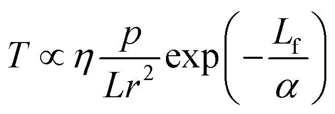
Fig. 1(a) shows the laser beam path diagram of the MPLI device. The KrF excimer laser (Coherent Inc. USA) has laser pulse duration and emitted wavelength of 25 ns and 248 nm, respectively. The processing parameters (i.e., laser power, laser spot size, and pulse frequency) require careful control to provide an appropriate temperature field on the sample surface. The laser beams are emitted horizontally from the KrF laser source and reflected downward by a reflection. The fluence of the laser spot on the NZO film can be easily adjusted by changing the value of L. Fig. 1(b) shows the thickness changes of the NZO film with different numbers of pulsed laser radiation (PLI) in atmospheric atmosphere at room temperature. Here, the laser fluence was adjusted to 60 mJ cm−2 and the frequency was set to 5 Hz. After MPLI, the thickness of the NZO was reduced by the laser ablation effect, as the surface temperature increases with increasing number of pulses.14 The average reduction rates of the A, B and C zones were 6.0, 1.375, and 3.65 nm per pulse, respectively. The film surface temperature can be expressed as12
 | (1) |
 | ||
| Fig. 1 (a) Schematic of the laser annealing setup; (b) thickness of NZO on quartz substrate with different numbers of pulsed laser radiation at room temperature. p-NZO and n-NZO denote p and n type ZnO:Na, respectively. | ||
 | ||
| Fig. 2 SEM images of the NZO film. (a) NZO; (b), (c), (d), (e), and (f) m-NZO with MPLI for 150, 250, 350, 450, and 650 times, respectively. | ||
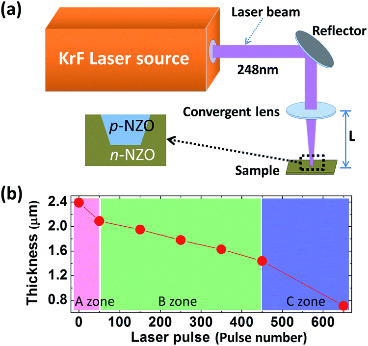
Fig. 2 shows SEM images of the NZO surface morphologies with different PLI times. Fig. 2(a), the a-NZO, shows an uneven surface, subsidence holes, and nonuniform crystal grain size, leading to η greater than 1.14 Fig. 2(b)–(f) show the laser-irradiated NZO with MPLI (m-NZO) 150, 250, 350, 450, and 650 times, respectively. The increasing numbers of pulses of laser irradiation cause the film surface to become flatter, as seen in Fig. 2(b)–(e). Increasing the MPLI up to 650 times results in NZO with extreme smooth and uniform crystal grain without crystal burrs (Fig. 2(f)). This is attributed to the high temperature, causing the ZnO crystal grains to melt down and recrystallize.15 The diameter of a crystal grain is ∼250 nm, as determined by the substrate's thermal conductivity, where higher conductivity gives larger final NZO crystal size.15
Fig. 3 shows the XRD patterns of a-NZO and m-NZO with MPLI of 150, 250, 350, and 650, respectively. Only the XRD peak corresponding to wurtzite ZnO (002) plane is seen, revealing the high crystallinity and c-axis preferential orientation of the NZO films.16 The mean crystallite size can be calculated using the Scherrer equation with full width at half-maximum (FWHM) of the (002) peak. This gives mean crystallite sizes of a-NZO, and m-NZO with 150, 250, 350, and 650 times MPLI of 12.790, 15.267, 15.055, 16.102, and 16.420 nm, respectively. Thus, the MPLI process increases the crystallite size and improves crystal quality, via the previously mentioned process of crystal grain meltdown and recrystallization.
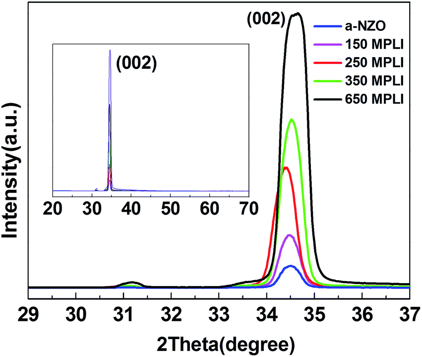 | ||
| Fig. 3 XRD patterns of a-NZO and m-NZO with different MPLI. | ||
Fig. 4(a) shows the carrier concentration and Hall mobility as a function of standing time of NZO at room temperature. This indicates that the a-NZO is p type; however, its hole concentration drops from 5.06 × 10¹⁹ to 9.15 × 1017 cm−3 within 50 minutes without any other treatment than the Hall testing. It then changes to n type within the next 50 minutes. Meanwhile, its carrier (electron) concentration increases up to 3.10 × 1019 cm−3 and the Hall mobility to 6.68 cm2 V−1 s−1. The above mentioned phenomenon demonstrates the unstable p type electrical property of the a-NZO.17 In fact, there is a high energy barrier (3.4 eV) for NaZn transformation to Nai, which is much higher than that (1.56 eV) of Nai to transform to a substitutional site.18 That is to say, NaZn is stable. Therefore, it is presumed that the initial p type conductivity of the a-NZO results from unstable p type defects rather than NaZn. When the NZO is annealed by MPLI for 150, 250, and 350 times, corresponding to points A, B, and C in Fig. 4(a), the temperature increases on the NZO surface. Meanwhile, the temperature decreases by ∼49% of the peak temperature (Tpeak) of each pulse in 600 ns, after which the next laser pulse comes. It can be calculated that after 30 laser pulses, the Tpeak would be higher than 1224 K.15 This is fairly close to the melting point of NZO; therefore, recrystallization of NZO is expected. After 150 pulses at A point in Fig. 4(a), the NZO film has experienced 150 cycles of rapid temperature increase and decrease processes, which provide sufficient thermodynamic energy for Na dopant to overcome the barrier energy from interstice site to substitutional site. The film then converts back to p type, as shown by the A, B, and C points. The hole concentration and Hall mobility reach up to 2.53 × 1019 cm−3 and 9.43 cm2 V−1 s−1, respectively, at C point. That is to say, the Hall mobility is better than that of the a-NZO, resulting in improved crystallographic quality after laser annealing treatment. After 5 days, the hole concentration and Hall mobility are maintained at 1.62 × 1019 cm−3 and 6.97 cm2 V−1 s−1. This demonstrates that the p type m-NZO has improved stability, which may arise from formation of NaZn. Fig. 4(b) shows the carrier concentration and Hall mobility of the m-NZO as a function of magnetic field intensity from 2 to 12 kG. It demonstrates good p type stability at different magnetic field intensities.
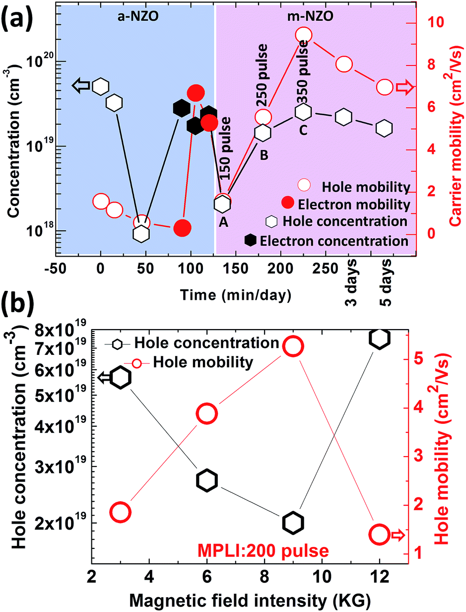 | ||
| Fig. 4 (a) Carrier concentration and Hall mobility as a function of standing time for NZO tested under 10 kG magnetic field intensity. The PLI times for A, B, and C are 150, 250, and 350, respectively. Red dot, white hexagon, and black filled hexagon denote Hall mobility, hole concentration, and electron concentration; (b) carrier concentration and Hall mobility of m-NZO as a function of magnetic field intensity from 2–12 kG. Red dot and white hexagon denote carrier Hall mobility and the holes concentration, respectively. | ||
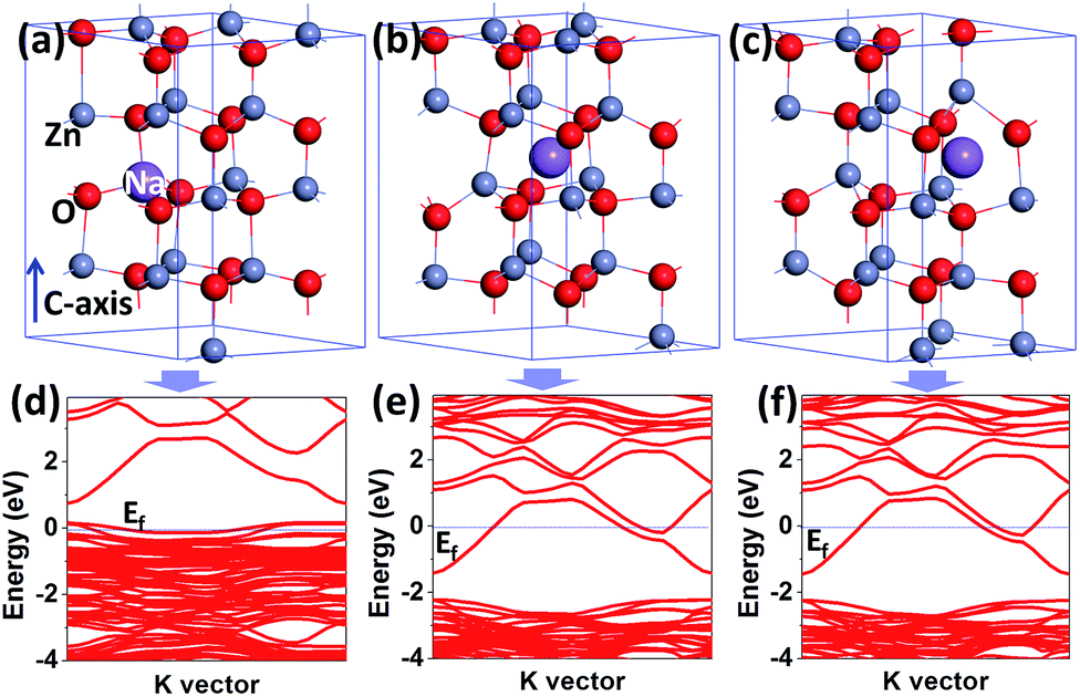
To characterize the optical properties of the NZO, PL was carried out at room temperature and low temperature (Fig. 5). Fig. 5(a) shows the normalized PL spectra at room temperature of a-NZO and m-NZO with MPLI for 0, 150, 250, and 350, and 650 times. All lines exhibit a dominant near-band-edge (NBE) emission, which is identified as the recombination of free exciton (FX).19 The strong NBE emission and negligible deep-level emission indicate that the obtained ZnO film is of high optical quality, which is suitable for application in electronic devices, while a wide deep-level emission (around 510 nm) related to the oxygen vacancies (VO) or intestinal zinc (Zni) is observed.20 As acting as donor will compensate the acceptor, the efficiency of Na doping is therefore reduced. In other words, more efficient p-type NZO film could be obtained by restraining the density of wide deep-level defects. It is noted that increasing the number of MPLI times corresponds to a weakening in intensity of the wide deep-level defect peak located at ∼510 nm, which demonstrates that the MPLI process improved the crystal quality and decreased the defect (VO and Zni) concentration dramatically. In Fig. 5(b), the red, black, green, and blue curves denote m-NZO, a-NZO, m-NZO after 5 days, and a-NZO after 5 days, respectively. The insert is normalized PL plots. The resulting PL spectra exhibit two dominant peaks centered at ∼3.35 (P1) and ∼3.21 eV (P2), which are assigned to the acceptor-bound (NaZn) exciton and donor–acceptor (NaZn) pairs (DAPs), respectively.21,22 The binding energy of an acceptor, EA, can be approximately calculated using the following eqn (2)21 (with the van der Pauw polarization interaction term neglected because of the relatively large value of r):
 | (2) |
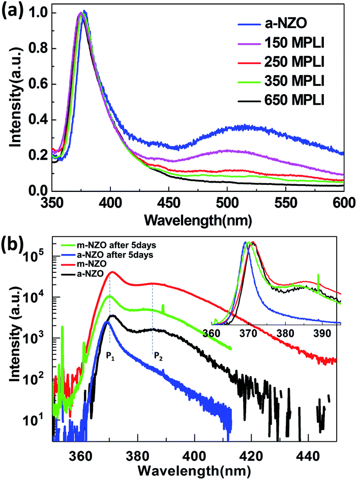 | ||
| Fig. 5 (a) Room-temperature PL spectra of a-NZO and m-NZO with MPLI for 0, 150, 250, and 350, and 650 times, respectively. (b) The low temperature (6 K) PL spectra of NZO at excitation power of 6 mW. The red, black, green, and blue curves denote m-NZO, a-NZO, m-NZO after 5 days, and a-NZO after 5 days, respectively. The inset shows a normalized PL plot. | ||
 | ||
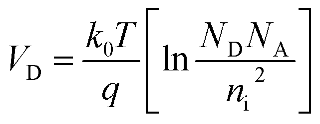
| Fig. 6 (a), (b) and (c) are geometry optimized models of NZO with Na at substitutional, tetrahedral interstice, and octahedral interstice sites. (d), (e) and (f) are the corresponding band structures. Ef is Fermi level. Red, grey, and purple balls denote O, Zn, and Na, respectively. | ||
Fig. 6(a)–(f) shows the geometry optimized models and corresponding band structures of NZO crystal. The Na atoms are located at substitutional, octahedral interstice (Naio), and tetrahedral interstice (Nait) sites, respectively, shown in Fig. 6(a)–(c). The position of the Fermi-level in the band structures indicates that ZnO:NaZn is p type and ZnO:Nait/io is n type, see Fig. 6(d)–(f).26,27 That is to say, p and n-ZnO could be obtained simply by doping Na elements, which gives theoretical support to the present work. The band gap energies are calculated to be 0.575, 0.796, and 0.789 eV for ZnO:NaZn, ZnO:Naio, and ZnO:Nait, respectively. These values are underestimated compared with experimental data, which is a well-known artifact of traditional density functional theory (DFT).18,28 The EA value from the first principle result is 165 meV, in good agreement with the experiment result of 161 meV from eqn (2).
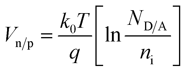
The room temperature current–voltage (I–V) curves of the p/n-NZO homojunction are shown in Fig. 7(a). Good rectifying behavior of the junction is observed from the I–V characteristics. Its turn on voltage appears at ∼2.47 V under forward bias voltage and the reverse breakdown voltage bias is ∼11.22 V. The inset Ia shows a photo of the p/n-NZO homojunction on a glass substrate with a laser ablated spot. The insets Ib and Ic demonstrate good ohmic behavior of the contact between A–B and C–D points, which confirms that the rectification arises from the NZO homojunction between A and C points. Fig. 7(b) shows the band structure of the p/n-NZO homojunction. VB and VD are the valence band and contact potential difference or threshold voltage. The VD of thermal equilibrium p–n junction can be expressed as:
 | ||
| Fig. 7 (a) The I–V curve of the p/n-NZO homojunction (between A and C points in the inset). The insets show a photo of the local laser-irradiated NZO homojunction (Ia), and the I–V curve of A–B and C–D points (Ib and Ic). (b) The band structure of the p/n-NZO homojunction. VB and VD are the valence band and contact potential difference. The blue dashed line is Fermi level of the p/n-NZO homojunction. | ||
Thus, Vn and Vp are 0.748 and 0.743 V, respectively. Then the φn and φp should be 1.197 and 1.189 eV. It is also noted that the turn on voltage (2.47 V) based on the I–V curve is far bigger than VD (1.49 V). This may be caused by the high resistance layer generated from the MPLI process in the interface of n- and p-NZA.
Conclusions
In summary, p/n-NZO homojunctions were prepared for on-chip integration purposes using a MPLI technique. The homojunction contains only Na dopants to realize p/n type conductivity of the ZnO film. The MPLI process can reduce the film thickness at ∼1.375 nm per pulse and improve the crystallinity by high temperature recrystallization. Meanwhile, it can also cause the Na dopants to occupy the substitutional sites of Zn to obtain more stable p type m-NZO than the a-NZO. The hole concentration and Hall mobility of the m-NZO are up to 2.53 × 1019 cm−3 and 9.43 cm2 V−1 s−1, respectively. The low temperature PL spectra at excitation power of 6 mW and the first principle calculation show that the acceptor energy level is ∼161 meV. The I–V curve of the p–n NZO homojunction shows good rectifying behavior, with a turn on voltage of ∼2.47 V under forward bias voltage and the reverse breakdown voltage bias ∼11.22 V. This convenient technique could be used in simplifying and improving controllability and accuracy in fabrication of microchip electronic devices.Acknowledgements
This work is supported by the National Natural Science Foundation of China (No. 11404138, 51401239, 21477047), China's Post-doctoral Science Fund (1100512), Shandong Provincial Natural Science Foundation of China (No. BS2014CL019, ZR2013BL002).Notes and references
- X. Y. Han, Y. H. Gao, J. N. Dai, C. H. Yu, Z. H. Wu, C. Q. Chen and G. J. Fang, J. Phys. D: Appl. Phys., 2010, 43(14), 145102 CrossRef.
- K. O. Hara, Y. Hoshi, N. Usami, Y. Shiraki, K. Nakamura, K. Toko and T. Suemasu, Thin Solid Films, 2013, 534, 470–473 CrossRef CAS.
- X. G. Han, J. N. Dai, C. H. Yu, Z. H Wu, C. Q. Chen and Y. H. Gao, Appl. Surf. Sci., 2010, 256(14), 4682–4686 CrossRef CAS.
- K. K. Ong, K. L. Pey, P. S. Lee, A. T. S. Wee, X. C. Wang and Y. F. Chong, Appl. Phys. Lett., 2006, 89, 172111 CrossRef.
- L. Rebohle, S. Prucnal and W. Skorupa, Semicond. Sci. Technol., 2016, 31, 103001 CrossRef.
- Y. F. Chong, K. L. Pey, A. T. S. Wee, A. See, L. Chan, Y. F. Lu, W. D. Song and L. H. Chua, Appl. Phys. Lett., 2000, 76, 3197–3199 CrossRef CAS.
- Y. Taur, C. H. Wann and D. J. Frank, Int. Electron Devices Meet., 1999, 789–792 Search PubMed.
- B. Yu, Y. Wang, H. H. Wang, Q. Xiang, C. Riccobene, S. Talwar and M. R. Lin, Int. Electron Devices Meet., 1999, 509–512 CAS.
- R. F. Wood, C. W. White, R. T. Young, E. K. Willardson and A. Beer, Semicond. Semimetals, 1984, vol. 23 Search PubMed.
- J. M. P. a. J. W. Mayer, Laser Annealing of Semiconductors, 1982 Search PubMed.
- D. Vanderbilt, Phys. Rev. B: Condens. Matter Mater. Phys., 1990, 41, 7892–7895 CrossRef.
- Y. Yan, G. M. Dalpian, M. M. Al-Jassim and S. H. Wei, Phys. Rev. B: Condens. Matter Mater. Phys., 2004, 70(19), 3352–3359 CrossRef.
- M. Y. Zhang and G. J. Cheng, J. Manuf. Sci. Eng., 2011, 133, 021010 CrossRef.
- M. Y. Zhang, Q. Nian and G. J. Cheng, Appl. Phys. Lett., 2012, 100, 151902 CrossRef.
- T. M. K. Thandavan, C. S. Wong, S. M. A. Gani and R. M. Nor, Mater. Express, 2014, 4, 475–482 CrossRef CAS.
- D. F. Urban, W. Körner and C. Elsässer, Phys. Rev. B: Condens. Matter Mater. Phys., 2016, 94, 075140 CrossRef.
- G. Zhang, L. Zheng, M. Zhang, S. Guo, Z. H. Liu, Z. Yang and Z. Wang, Energy Fuels, 2012, 26, 618–623 CrossRef CAS.
- W. Chen, X. H. Pan, S. S. Chen, H. P. He, J. Y. Huang, B. Lu and Z. Z. Ye, Appl. Phys. A: Mater. Sci. Process., 2015, 121, 77–82 CrossRef CAS.
- H. Y. Lin, C. L. Cheng, Y. Y. Chou, L. L. Huang and Y. F. Chen, Opt. Express, 2006, 14, 2372 CrossRef CAS PubMed.
- F. X. Xiu, Z. Yang, L. J. Mandalapu, D. T. Zhao, J. L. Liu and W. P. Beyermann, Appl. Phys. Lett., 2005, 87, 152101 CrossRef.
- S. S. Lin, J. G. Lu, Z. Z. Ye, H. P. He, X. Q. Gu, L. X. Chen, J. Y. Huang and B. H. Zhao, Solid State Commun., 2008, 148, 25–28 CrossRef CAS.
- S. S. Lin, Appl. Phys. Lett., 2012, 101, 122109 CrossRef.
- X. P. Yang, J. G. Lu, H. H. Zhang, Y. Chen, B. T. Kan, J. Zhang, J. Huang, B. Lu, Y. Z. Zhang and Z. Z. Ye, Chem. Phys. Lett., 2012, 528, 16–20 CrossRef CAS.
- Z. Ye, T. Wang, S. Wu, X. Ji and Q. Zhang, J. Alloys Compd., 2017, 690, 189–194 CrossRef CAS.
- M. Khuili, N. Fazouan, H. A. El Makarim, G. El Halani and E. H. Atmani, J. Alloys Compd., 2016, 688, 368–375 CrossRef CAS.
- L. H. Li, Y. B. Lv, J. Z. Li and K. Yu, J. Alloys Compd., 2014, 617, 102–107 CrossRef.
- D. Segev, A. Janotti and C. G. van de Walle, Phys. Rev. B: Condens. Matter Mater. Phys., 2007, 75(3), 035201 CrossRef.
- Y. W. H. D. P. Norton, M. P. Ivill, K. Ip, S. J. Pearton, M. F. Chisholm and T. Steiner, Mater. Today, 2004, 7, 7 CrossRef.
| This journal is © The Royal Society of Chemistry 2017 |