
 Open Access Article
 This Open Access Article is licensed under a
 Creative Commons Attribution 3.0 Unported Licence
Highly active and porous single-crystal In2O3 nanosheet for NOx gas sensor with excellent response at room temperature†
Li Sunab,
Wencheng Fanga,
Ying Yang *a,
Hui Yua,
Tingting Wanga,
Xiangting Dong*a,
Guixia Liua,
Jinxian Wanga,
Wensheng Yua and
Keying Shi*c
*a,
Hui Yua,
Tingting Wanga,
Xiangting Dong*a,
Guixia Liua,
Jinxian Wanga,
Wensheng Yua and
Keying Shi*c
aKey Laboratory of Applied Chemistry and Nanotechnology at Universities of Jilin Province, Changchun University of Science and Technology, Changchun 130022, China. E-mail: yangying0807@126.com; dongxiangting888@163.com; Fax: +86 0431 85383815; Tel: +86 0431 85582574
bCollege of Chemistry and Chemical Engineering, Qiqihar University, Qiqihar 161006, P. R. China
cKey Laboratory of Functional Inorganic Material Chemistry (Heilongjiang University), Ministry of Education, Harbin 150080, P. R. China. E-mail: shikeying2008@163.com
First published on 3rd July 2017
Abstract
Porous single-crystal In2O3 nanosheet (ps-In2O3 NS) was designed and prepared through a method of calcination after liquid reflux. Compared with the other In2O3 with different surface morphologies, the ps-In2O3 NS has gas sensing properties towards NOx at room temperature. Gas sensing data strongly demonstrate that this porous single-crystal In2O3 nanosheet exhibits a distinguished response (89.48) and fast response time (16.6 s) to 97.0 ppm NOx. Meanwhile, the ps-In2O3 NS sensor presents a favorable linearity and good selectivity, and the detection of NOx is down to ppb levels at room temperature. The enhancement of the sensing response is attributed to the porous, single-crystal and two dimensional nanosheet structure of the synthesized ps-In2O3 NS, which has much higher BET surface area, effective gas diffusion of slit pores and thus provides more active sites for the reaction of NOx with surface-adsorbed oxygen ions. This work would be important for the low-cost and high performance of the In2O3 material with highly promising applications in gas sensors.
Introduction
Chemical sensing based on various nanostructures1,2 has attracted enormous attentions, as that is widely perceived as one of the most promising fields for nanotechnology to generate significant impact. Among the chemicals studied, NO and NO2 (NOx) are amongst the most dangerous air pollutants, which play major roles in the formation of ozone and acid rain.3,4 Continued or frequent exposure to NOx concentrations higher than the air quality standard (53 ppb) may cause increased incidence of acute respiratory illness in children.5 The detection and measurement of NOx gas are thus of great importance in both environmental protection and human health.Semiconducting metal oxides, such as, In2O3,6,7 SnO2,8,9 CuO,10,11 ZnO12,13 and Fe3O4 (ref. 14) have been extensively studied as chemical sensing materials due to their extraordinary properties, such as good response, short response time and selectivity to the ambient conditions in addition to the simplicity in materials synthesis and sensing device fabrication.15,16 Among the semiconducting metal oxides, In2O3, an important functional semiconductor material with remarkable electronic properties, which has been proven to be a very good candidate with a pronounced response to detect chemicals like NOx,17 NH3,18 ethanol,19 H2S,20 acetone,21 formaldehyde,22,23 Cl2 (ref. 24) and so on, has attracted considerable interest for several decades. A great attention has been recently paid to the development of new material “architectures” based on In2O3 at the nano-scale.25,26 Since detection of a given gas involves adsorption process on the surface of the sensing material, it is expected that the higher the surface, the greater the sensor response. Thus, it is quite essential to control the size, shape, and surface characteristics of the sensing material in order to achieve reliable properties.27,28 Two-dimensional (2D) and porous oxide provide a high surface area for chemical reaction, effective diffusion of gases species into the interface/surface, and enhance gas sensing performance.29 Various synthetic strategies to prepare 2D and porous structures for gas sensor applications have been reported.30 Compared with the other methods, such as vapor phase, the hydrothermal method are proven to be environmentally benign methods, which are able to produce In2O3 nanostructures in mass quantities.31,32 But, 2D porous single-crystal In2O3 nanosheet have not yet been reported. Our research is focused on enhancing the material surface area while keeping a high crystalline degree of the nano-structured In2O3.
In this paper, we reported the synthesis of porous single-crystal In2O3 nanosheet by calcinations of In(OH)3 for the first time. During the synthesis, urea was used as an alkaline source and ligand for assembling the porous and single crystal nanosheet. The as-obtained ps-In2O3 NS was applied as a high performance gas sensor to detect NOx down to 485 ppb, one order of magnitude better than the previously fabricated In2O3 nanosheet NOx sensors at room temperature, suggesting a great potential in sensing related application.
Experimental
Sample preparation
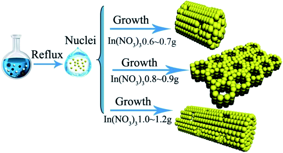
The porous single-crystal In2O3 nanosheet (ps-In2O3 NS) were fabricated by a facile liquid reflux method with In(NO3)3, urea and SDBS as In source, precipitant and the structure-director, respectively. The process is schematically illustrated in Scheme 1. Typically, In(NO3)3 (0.90 g), urea (0.80 g), SDBS (0.17 g) and H2O (50 mL) were added into a beaker reservoir and then stirred vigorously for 1 h. The homogenous mixture was refluxed at 100 °C for 3 h in a flask to obtain the precursor of ps-In2O3 NSs. Subsequently, the precursor was heated to 550 °C for 4 h in air with a heating rate of 2 °C min−1. After naturally cooling to room temperature, the ps-In2O3 NS sample was obtained. Different dosage of In(NO3)3 (0.6 g, 0.7 g, 0.8 g, 0.9 g, 1.0 g and 1.2 g) was marked as In2O3-0.6, In2O3-0.7, In2O3-0.8, In2O3-0.9, In2O3-1.0 and In2O3-1.2, while other reaction conditions are the same as that described above.
 | ||
| Scheme 1 The formation mechanism of the different porous In2O3. | ||
Material characterizations
The X-ray diffraction (XRD) patterns were examined by using an X-ray diffractometer (XRD, Bruker NEW D8 ADVANCE, Germany) with monochromatized Cu-Kα radiation with an accelerating voltage of 40 kV and an applied current of 20 mA. The morphologies and structures of the ps-In2O3 NS were observed by scanning electron microscope (SEM, HITACHI S-4800) and transmission electron microscopy (TEM, JEOL-2100). X-Ray photoelectron spectra (XPS) were recorded with a AXIS ULPRA DLD (Shimadzu Corporation) system equipped to analyze the surface composition of porous single-crystal In2O3 nanosheet, using monochromatic Al Kα radiation (1486.4 eV), and C 1s (284.6 eV) was utilized as a reference to correct the binding energy. The nitrogen adsorption/desorption isotherms were measured at 77 K using a Micromeritics Tristar II. The BET surface area was analyzed by Brunauer–Emmett–Teller (BET) theory. The pore size distribution was computed by the nonlocal density functional theory (NLDFT) method.Fabrication and measurements of gas sensors
An interdigitated Au electrode (7 × 5 × 0.38 mm) was selected for the gas sensing detection and the electrode spacing was 20 μm. The sample materials were spin-coated onto the interdigital electrode to form a sensitive film and then dried at 70 °C for 5 h to obtain a gas sensor. The sensor was installed into a test chamber with an inlet and an outlet. The electrical resistance measurements of the sensor were carried out at room temperature and a relative humidity (RH) around 40%. The NOx gas concentration was controlled by injecting volume of the gas and the chamber was purged with air to recover the sensor resistance. The gas response can be obtained from eqn (1).33,34| Response (R) = (RN − R0)/R0 | (1) |
The response time is defined as the time required for the variation in resistance to reach 85% of the equilibrium value after a test gas was injected. The test was conducted at room temperature (20 °C) with a relative humidity (RH) around 40%.
Results and discussion
Structure, morphology characterization of ps-In2O3 NS
Porous single-crystal In2O3 nanosheet (ps-In2O3 NS) were synthesized by calcinating In(OH)3 precursors. The phase transformation process of the In(OH)3 sample during calcinations in air was studied via TG-DSC (Fig. S1†). It is observed that the decomposition started at 200 °C in the TG curve of In(OH)3. The TG-DSC curve indicates an endothermic reaction around 260 °C. The In(OH)3 directly converts into cubic phase of In2O3 in our experiment at 290 °C. If a temperature higher than 550 °C was chosen, the nanosheets shapes were destroyed and only In2O3 nanoparticles were obtained. Hence, the annealing temperature is ascertained to be 550 °C in order to obtain pure In2O3 nanosheets.Fig. 1a shows a typical TEM image of the ps-In2O3 NS, in which the annealed In2O3 are porous nanosheet with a rough surface and many tiny pores with diameters of several nanometres exist along the whole area of the nanosheet. To further examine the surface morphology of the nanosheet, high-magnification TEM images were recorded, as shown in Fig. 1b and c. The selected-area electron diffraction (SAED) pattern (lower left inset of Fig. 1c) has confirmed this structure with single crystalline nature. The HR-TEM image of ps-In2O3 NS is displayed in Fig. 1d. The fringe spacing is about 0.29 nm, corresponding to the (222) crystal planes of the cubic In2O3.
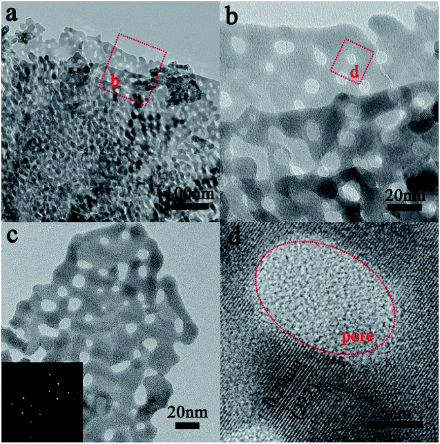 | ||
| Fig. 1 (a–c) Representative TEM images of the synthesized ps-In2O3 NS, the inset shows the SAED pattern of the ps-In2O3 NS; (d) HRTEM image of ps-In2O3 NS, in which the (222) of cubic phase In2O3 can been seen. | ||
Fig. 2a shows the powder X-ray diffraction (XRD) pattern of the In(OH)3 precursor. All diffraction peaks are sharp and well-defined, suggesting that the sample is highly crystallized. The peaks at 2θ values of 31.8, 34.4, 36.3, 47.5, 56.6, 62.9 and 68.1° are consistent with the cubic phase In(OH)3 (JCPDS no. 76-1464).35 The XRD pattern of the annealed ps-In2O3 NS is depicted in Fig. 2b. All of the detectable peaks in the pattern can be easily indexed to pure cubic In2O3 phase with a = b = c = 10.140 Å, in good agreement with the standard data (JCPDS no. 65-3170),36 confirming that this product is pure In2O3 with a cubic structure. No other diffraction peaks related to impurities are observed, indicating the formation of pure cubic In2O3.
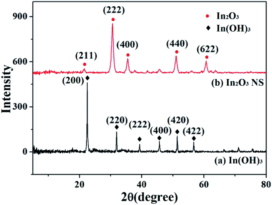 | ||
| Fig. 2 XRD patterns of (a) the In(OH)3 precursors, and (b) the synthesized ps-In2O3 NS. | ||
In this synthesis, the indium ion concentration plays an important role in formation of different morphology In2O3. It can be seen that when the indium ion concentration is low (indium precursor of 0.6 g or 0.7 g seen in Fig. 3a and b and S2a and b†), In2O3 mainly are porous nanoparticles (NPs) with a rough surface and many tiny pores exist along the NPs. However, assembling of In2O3 occurred, when further increasing the indium precursor to 0.8 g seen in Fig. 3c, and S3a and b.† When indium precursor is increased to 0.9 g shown in Fig. 3d, the ps-In2O3 NS has been synthesized. But, when further increasing the mass of the indium precursor to 1.0 g or 1.2 g seen in Fig. 3e and f and S4a and b,† the nanorods-like In2O3 formed with many pores on the surface. These different morphologies of In2O3 will affect the properties of gas sensing.
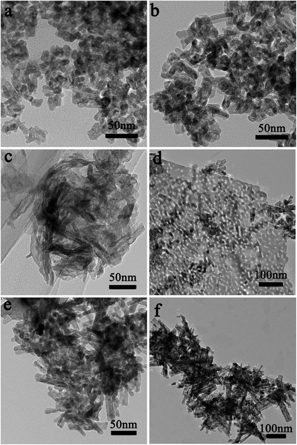 | ||
| Fig. 3 Representative TEM images of the synthesized In2O3 with different In(NO3)3, (a) 0.6 g, (b) 0.7 g, (c) 0.8 g, (d) 0.9 g, (e) 1.0 g and (f) 1.2 g. | ||
The different morphology structures of In2O3 prepared with different contents of In(NO3)3 is also studied by nitrogen adsorption–desorption measurement at 77 K. The N2 adsorption desorption isotherm and pore size distribution curves of the typical synthesized In2O3 samples are shown in Fig. 4 and Table S1.† The Brunauer–Emmett–Teller (BET) surface area and total pore volume are 44.85 m2 g−1 and 0.28 cm3 g−1, respectively. In detail, the isotherm of ps-In2O3 NS exhibits typical type IV curve with H2 hysteresis loop. The pore size distribution exhibited in set of Fig. 4d also demonstrated multiple pore structure, and the average pore size about 25.51 nm. The large surface area and plentiful pores of ps-In2O3 NS can provide large accessible area for gas adsorption and desorption.
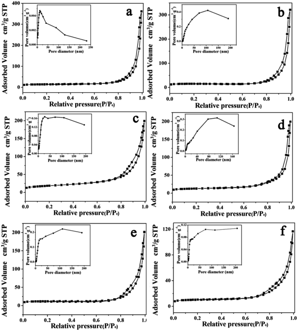 | ||
| Fig. 4 Nitrogen adsorption–desorption isotherm and the corresponding pore size distribution (inset) of the synthesized In2O3 with different In(NO3)3 addition: (a) 0.6, (b) 0.7 (c) 0.8, (d) 0.9, (e) 1.0 and (f) 1.2. | ||
Gas sensing performances and sensing mechanism
It is known that the response of the gas sensors is mainly related to the gas concentration. To study the gas sensor properties of the ps-In2O3 NS sensor, series of experiments were carried out by varying the NOx gas concentration from 97.0–0.485 ppm. Fig. 5a shows the representative response–recovery cyclic curves for a the synthesized ps-In2O3 NS sensor to 97.0–0.485 ppm NOx operated at room temperature. The resistance signal represents the increase from the background resistance R0 to an equilibrium value RN when the NOx gas enters the test chamber, and restores to the background value when pure air enters the chamber. Finally, the almost complete recovery of the baseline resistance values at the end of each pulse indicated a reversible interaction between the sensing element and the target analytes, a key issue in view of eventual technological applications.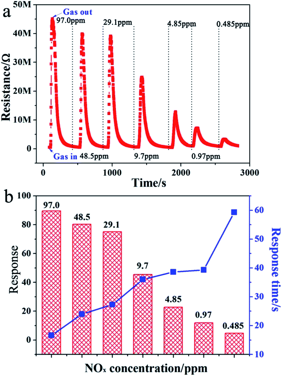 | ||
| Fig. 5 The results of the gas response of the synthesized ps-In2O3 NS sensor to 97.0–0.485 ppm NOx operated at room temperature. (a) The representative response–recovery cyclic curves; (b) corresponding response and response time curves. | ||
Response to NOx was obtained from the calculation of resistance value by using eqn (1).37 According experimental results, the resistance increased when NOx contacts the ps-In2O3 NS surface. The ps-In2O3 NS is a N-type (electron conductivity) semiconductor. Similar results were obtained by Keying Shi and co-workers38 using a N-type SnO2–In2O3 composite sensing material. Fig. 5b shows the corresponding relationship between response and response time under different NOx concentrations. When the concentration of NOx is 97.0 ppm, the response time is only 16.6 s, while the highest response reached is 89.48. It is found that response declined gradually with the decreased concentration of NOx. The limitation of NOx detection reaches as low as 485 ppb, and the response increases with the increasing gas concentration, which means the sensor is suitable for detecting a wide concentration range of NOx. Compared with the gas response and response time of the In2O3-0.7, In2O3-0.8, In2O3-0.9, In2O3-1.0 and In2O3-1.2, In2O3-0.9 shows the best gas sensing performance (in Tables S2 and S3†). Moreover, we list the literatures about the gas sensing device that detect NOx (NO or NO2) sensing in Table S4.† It is observed that the gas sensing based on ps-In2O3 NS shows a low working temperature (room temperature), short response time and low detection limit. The detailed data would be seen in Table S2† (In2O3-0.9).
Fig. 6a shows response changes as the NOx concentration varies from 97.0–0.485 ppm. It was revealed that the linearity of the line formed by plotting log![[thin space (1/6-em)]](https://www.rsc.org/images/entities/char_2009.gif) R (response) against NOx was R2 = 0.94379. In view of practical applications, the sensor selectivity is a key concern and, at the same time, we measured the response to some gases such as NOx, O2, NH3, H2, C2H2 and CO at room temperature. As shown in Fig. 6b, the ps-In2O3 NS sensor exhibits an excellent selectivity for NOx, and no response to O2, NH3, H2, C2H2 and CO. The ps-In2O3 NS sensor thus is suitable for application to commercial NOx sensing systems.
R (response) against NOx was R2 = 0.94379. In view of practical applications, the sensor selectivity is a key concern and, at the same time, we measured the response to some gases such as NOx, O2, NH3, H2, C2H2 and CO at room temperature. As shown in Fig. 6b, the ps-In2O3 NS sensor exhibits an excellent selectivity for NOx, and no response to O2, NH3, H2, C2H2 and CO. The ps-In2O3 NS sensor thus is suitable for application to commercial NOx sensing systems.
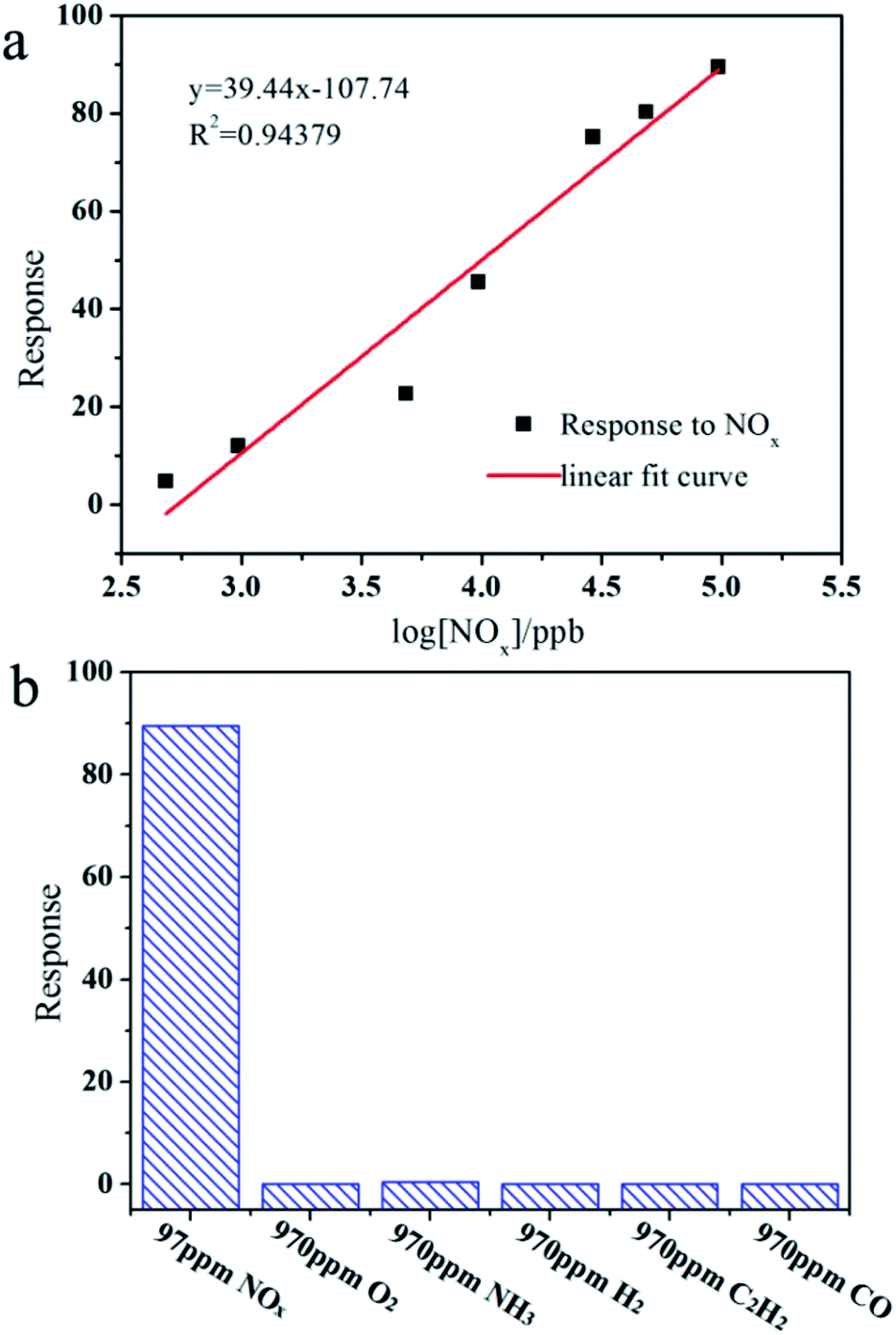 | ||
| Fig. 6 (a) The histogram of the response for the ps-In2O3 NS sensor to different gases at room temperature; (b) linear dependence relation between the response and relative NOx concentration for ps-In2O3 NS sensor. | ||
When the N-type In2O3 semiconductor is used in gas sensor and exposed in air, O2 molecules will be chemisorbed and can trap the electrons of the In2O3 to be changed into O2−, O−, and O2− on the In2O3 surfaces.39–41 Such chemisorbed oxygen is suggested to act as an electron donor, which depend strongly on temperature and the nature of the material. The formation of numerous oxygen species (e.g. O2−, O−, and O2−), which are known for their good catalytic activity in gas sensors, could improve the performance of NOx sensor.42,43 After the oxidizing gas (e.g. NOx) is introduced, some oxygen species will be reduced and removed from the surfaces above a certain temperature, resulting in the variation of the resistance of In2O3. The surface area and the morphology of a sensing film can directly decide the adsorption quantity of the oxygen species and hence have important impacts on the variation of resistance and the relevant response of the sensors. The Schematic for sensing mechanism is shown in Scheme 2. When the sensor film is exposed to NOx, the NOx gas molecules could attract the electrons from which results in an increase of the In2O3 sensor, because the In2O3 sensor is a N-type semiconductor. It finally results in the rapid increase of the resistance (Scheme 2). The target gas molecules (NO2) directly adsorb onto In2O3 and react with O− the In2O3 because of the high electron affinity of the NOx molecules, which leads to electron transfer from the In2O3 to the NOx. The adsorption of NO2 on In2O3 leads to NO2− and the adsorption of NO on In2O3 leads to NO−.44,45 The process traps electrons from the conduction band or donor level of In2O3, and generate bidentate NO3−.5,46 The target gas molecules (NO) also can adsorb onto In2O3 and react with O− and generate NO2−.6
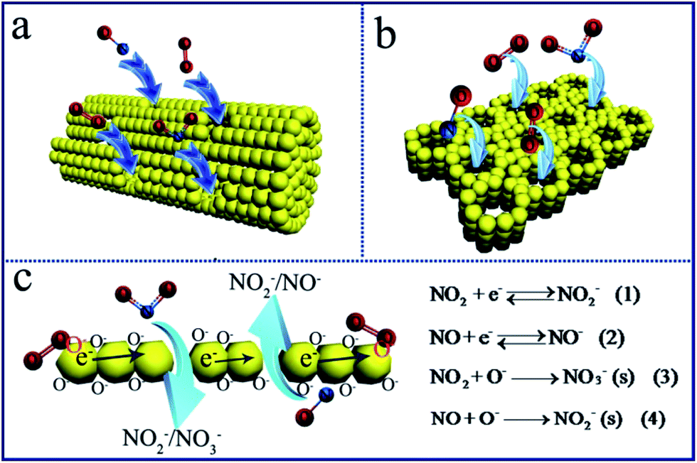 | ||
| Scheme 2 The gas sensing mechanism of the different porous In2O3 sensors. | ||
From all the above, the good gas sensing for NOx of the In2O3 sensor can be ascribed to the following two factors. First, effective gas diffusion and contact from pores of the In2O3 may also contribute to the good gas sensing. The porous structure can act as channels for gas diffusion, and thus provide more active sites for the reaction of NOx with surface-adsorbed oxygen ions. Second, the good gas sensing for NOx of the In2O3 sensor can be ascribed to the single crystal In2O3 and its own nanosheet structure which have a beneficial effect on the performance of the In2O3 sensor.47,48 The ideal structure is considered to be single crystal, because such gas sensing materials can exhibit high electron conductivities, and have abundant interfacial active sites and excellent stability.49,50 When the porous coupled with single crystallinity provides for the ease of gas diffusion and more active sites for the formation of reactive oxygen species.51 Then the oxygen species are benefit to the gas sensing performance. So the single crystal structure will lead to good gas sensing performance. These factors improve the performance of the ps-In2O3 NS sensor together.
Conclusions
In summary, we have demonstrated that the porous single-crystal In2O3 nanosheet via a liquid reflux method. The ps-In2O3 NS have gas sensing properties towards NOx and gas sensing data shows this porous single-crystal In2O3 nanosheet exhibit an excellent response (89.48), fast response time (16.6 s) and low testing limit to the NOx at room temperature, respectively. The good gas sensing is attributed to the effective gas diffusion and contact by the pore cannals on the surface of the In2O3 nanosheet.Acknowledgements
We gratefully acknowledge the support of this research by the National Natural Science Foundation of China (No. 21601018, 21401012, 51573023, 51572034, 21501104, 21501014), the Natural Science Foundation of Heilongjiang Province (B2015014), the Natural Science Foundation of Changchun University of Science and Technology (No. XQNJJ-2015-07), the University Nursing Program for Young Scholars with Creative Talents in Heilongjiang Province (UNPYSCT-2016088), the Open Project Foundation of Key Laboratory of Functional Inorganic Material Chemistry (Heilongjiang University).Notes and references
- (a) Y. H. Hang and H. E. Katz, J. Mater. Chem. C, 2017, 5, 2160–2166 RSC; (b) Y. L. Guo, T. Wang, F. H. Chen, X. M. Sun, X. F. Li, Z. Z. Yu, P. B. Wan and X. D. Chen, Nanoscale, 2016, 8, 12073–12080 RSC.
- J. Zhang, Z. Y. Qin, D. W. Zeng and C. S. Xie, Phys. Chem. Chem. Phys., 2017, 19, 6313–6329 RSC.
- Z. M. Liu, H. Y. Liu, H. Zeng and Q. Xu, Catal. Sci. Technol., 2016, 6, 8063–8071 CAS.
- Z. J. Feng, J. Q. Wang, X. Liu, Y. W. Wen, R. Chen, H. F. Yin, M. Q. Shen and B. Shan, Catal. Sci. Technol., 2016, 6, 5580–5589 CAS.
- J. Gao, H. Y. Wu, J. Zhou, L. Y. Yao, G. Zhang, S. Xu, Y. Xie, L. Li and S. Y. Shi, New J. Chem., 2016, 40, 1306–1311 RSC.
- L. Y. Yao, K. Kan, Y. F. Lin, J. B. Song, J. C. Wang, J. Gao, P. K. Shen, L. Li and K. Y. Shi, RSC Adv., 2015, 5, 15515–15523 RSC.
- X. M. Xu, H. J. Zhang, C. Z. He, C. Y. Pu, Y. M. Leng, G. Q. Li, S. J. Hou, Y. S. Zhu, L. Fu and G. Y. Lu, RSC Adv., 2016, 6, 47083–47088 RSC.
- J. B. Sun, P. Sun, D. L. Zhang, J. Xu, X. S. Liang, F. M. Liu and G. Y. Lu, RSC Adv., 2014, 4, 43429–43435 RSC.
- P. Sun, X. Zhou, C. Wang, K. Shimanoe, G. Y. Lu and N. Yamazoe, J. Mater. Chem. A, 2014, 2, 1302–1308 CAS.
- N. B. Tanvir, O. Yurchenko, C. Wilbertz and G. Urban, J. Mater. Chem. A, 2016, 4, 5294–5302 CAS.
- Z. Li, C. K. Dong, J. Yang, S. Z. Qiao and X. W. Du, J. Mater. Chem. A, 2016, 4, 2699–2704 CAS.
- J. C. Liao, Z. C. Li, G. J. Wang, C. H. Chen, S. S. Lv and M. Y. Li, Phys. Chem. Chem. Phys., 2016, 18, 4835–4841 RSC.
- N. Qin, Q. Xiang, H. B. Zhao, J. C. Zhang and J. Q. Xu, CrystEngComm, 2014, 16, 7062–7073 RSC.
- T. Y. Yang, L. Y. Du, C. B. Zhai, Z. F. Li, Q. Zhao, Y. Luo, D. J. Xing and M. Z. Zhang, J. Alloys Compd., 2017, 718, 396–404 CrossRef CAS.
- Y. Yang, C. G. Tian, J. C. Wang, L. Sun, K. Y. Shi, W. Zhou and H. G. Fu, Nanoscale, 2014, 6, 7369–7378 RSC.
- H. Y. Wu, L. L. Wang, J. Zhou, J. Gao, G. Zhang, S. Xu, Y. Xie, L. Li and K. Y. Shi, J. Colloid Interface Sci., 2016, 466, 72–79 CrossRef CAS PubMed.
- X. M. Xu, X. Li, H. J. Zhang, C. H. Feng, C. Wang, F. M. Liu, Y. F. Sun, P. Sun and G. Y. Lu, RSC Adv., 2015, 5, 30297–30302 RSC.
- H. F. Yang, X. Zhang, J. F. Li, W. T. Li, G. C. Xi, Y. Yan and H. Bai, Microporous Mesoporous Mater., 2014, 200, 140–144 CrossRef CAS.
- W. H. Zhang, W. C. Zhang, B. Chen, R. Shao, R. F. Guan, W. D. Zhang, Q. F. Zhang, G. H. Hou and L. Yue, Sens. Actuators, B, 2017, 239, 270–278 CrossRef CAS.
- Y. Y. Wang, G. T. Duan, Y. D. Zhu, H. W. Zhang, Z. K. Xu, Z. F. Dai and W. P. Cai, Sens. Actuators, B, 2016, 228, 74–84 CrossRef CAS.
- X. S. Liang, G. X. Jin, F. M. Liu, X. S. Zhang, S. S. An, J. Ma and G. Y. Lu, Ceram. Int., 2015, 41, 13780–13787 CrossRef CAS.
- J. Wang, X. P. Gan, Z. Y. Li and K. C. Zhou, Powder Technol., 2016, 303, 138–146 CrossRef CAS.
- L. T. Ma, H. Q. Fan, H. L. Tian, J. W. Fang and X. Z. Qian, Sens. Actuators, B, 2016, 222, 508–516 CrossRef CAS.
- P. Li and H. Q. Fan, Mater. Sci. Semicond. Process., 2015, 29, 83–89 CrossRef CAS.
- X. Y. Bai, W. J. Ji, S. N. Li, Y. C. Jiang, M. C. Hu and Q. G. Zhai, Cryst. Growth Des., 2017, 17, 423–427 CAS.
- Y. Ren, X. R. Zhou, W. Luo, P. C. Xu, Y. H. Zhu, X. X. Li, X. W. Chang, Y. H. Deng and D. Y. Zhao, Chem. Mater., 2016, 28, 7997–8005 CrossRef CAS.
- X. H. Sun, H. R. Hao, H. M. Ji, S. Cai and C. M. Zheng, ACS Appl. Mater. Interfaces, 2014, 6, 401–409 CAS.
- A. Shanmugasundaram, P. Basak, S. V. Manorama, B. Krishna and S. Sanyadanam, ACS Appl. Mater. Interfaces, 2015, 7, 7679–7689 CAS.
- S. Y. Choi, Y. H. Kim, H. S. Chung, A. R. Kim, J. D. Kwon, J. Park, Y. L. Kim, S. H. Kwon, M. G. Hahm and B. Cho, ACS Appl. Mater. Interfaces, 2017, 9, 3817–3823 CAS.
- M. Zhang, G. X. Feng, Z. G. Song, Y. P. Zhou, H. Y. Chao, D. Q. Yuan, T. T. Y. Tan, Z. G. Guo, Z. G. Hu, B. Z. Tang, B. Liu and D. Zhao, J. Am. Chem. Soc., 2014, 136, 7241–7244 CrossRef CAS PubMed.
- B. A. Prakasam, M. Lahtinen, A. Peuronen, M. Muruganandham and M. Sillanpää, Mater. Chem. Phys., 2016, 184, 183–188 CrossRef.
- A. Qurashi, J. A. Rather, T. Yamazaki, M. Sohail, K. D. Wael, B. Merzougui and A. S. Hakeem, Sens. Actuators, B, 2015, 221, 167–171 CrossRef CAS.
- B. F. Wu, L. L. Wang, H. Y. Wu, K. Kan, G. Zhang, Y. Xie, Y. Tian, L. Li and K. Y. Shi, Microporous Mesoporous Mater., 2016, 225, 154–163 CrossRef CAS.
- H. X. Sun, Z. Y. Chu, D. H. Hong, G. Zhang, Y. Xie, L. Li and K. Y. Shi, J. Alloys Compd., 2016, 658, 561–568 CrossRef CAS.
- J. J. Liu, G. Chen, Y. G. Yu, Y. L. Wu, M. J. Zhou, H. Q. Zhang, C. D. Lv, H. Qin and X. Qi, RSC Adv., 2016, 6, 14615–14619 RSC.
- S. Li, Z. F. Shi, Z. J. Tang and X. J. Li, J. Alloys Compd., 2017, 705, 198–204 CrossRef CAS.
- W. Yang, P. Wan, X. D. Zhou, J. M. Hu, Y. F. Guan and L. Feng, ACS Appl. Mater. Interfaces, 2014, 6, 21093–21100 CAS.
- S. Xu, J. Gao, L. L. Wang, K. Kan, Y. Xie, P. K. Shen, L. Li and K. Y. Shi, Nanoscale, 2015, 7, 14643–14651 RSC.
- H. Y. Wu, K. Kan, L. L. Wang, G. Zhang, Y. Yang, H. Li, L. Q. Jing, P. K. Shen, L. Li and K. Y. Shi, CrystEngComm, 2014, 16, 9116–9124 RSC.
- P. Li, H. Q. Fan, Y. Cai, M. M. Xu, C. B. Long, M. M. Li, S. H. Lei and X. W. Zou, RSC Adv., 2014, 4, 15161–15170 RSC.
- R. Q. Xing, Q. L. Li, L. Xia, J. Song, L. Xu, J. H. Zhang, Y. Xie and H. W. Song, Nanoscale, 2015, 7, 13051–13060 RSC.
- S. Park, S. Kim, G. J. Sun and C. Lee, ACS Appl. Mater. Interfaces, 2015, 7, 8138–8146 CAS.
- L. L. Wang, J. Gao, B. F. Wu, K. Kan, S. Xu, Y. Xie, L. Li and K. Y. Shi, ACS Appl. Mater. Interfaces, 2015, 7, 27152–27159 CAS.
- M. Q. Huang, Z. D. Cui, X. J. Yang, S. L. Zhu, Z. Y. Li and Y. Q. Liang, RSC Adv., 2015, 5, 30038–30045 RSC.
- Q. Y. Yang, X. B. Cui, J. Y. Liu, J. Zhao, Y. L. Wang, Y. Gao, P. Sun, J. Ma and G. Y. Lu, New J. Chem., 2016, 40, 2376–2382 RSC.
- J. Gao, L. L. Wang, K. Kan, S. Xu, L. Q. Jing, S. Q. Liu, P. K. Shen, L. Li and K. Y. Shi, J. Mater. Chem. A, 2014, 2, 949–956 CAS.
- Z. P. Li, H. Yan, S. L. Yuan, Y. J. Fan and J. H. Zhan, J. Colloid Interface Sci., 2011, 354, 89–93 CrossRef CAS PubMed.
- J. Rombach, A. Papadogianni, M. Mischo, V. Cimalla, L. Kirste, O. Ambacher, T. Berthold, S. Krischok, M. Himmerlich, S. Selve and O. Bierwagen, Sens. Actuators, B, 2016, 236, 909–916 CrossRef CAS.
- L. J. Guo, X. P. Shen, G. X. Zhu and K. M. Chen, Sens. Actuators, B, 2011, 155, 752–758 CrossRef CAS.
- S. Elouali, L. G. Bloor, R. Binions, I. P. Parkin, C. J. Carmalt and J. A. Darr, Langmuir, 2012, 28, 1879–1885 CrossRef CAS PubMed.
- J. J. Liu, G. Chen, Y. G. Yu, Y. L. Wu, M. J. Zhou, H. Q. Zhang, C. D. Lv, H. Qin and X. Qi, RSC Adv., 2016, 6, 14615–14619 RSC.
Footnote |
| † Electronic supplementary information (ESI) available. See DOI: 10.1039/c7ra05446g |
| This journal is © The Royal Society of Chemistry 2017 |