
 Open Access Article
 This Open Access Article is licensed under a
 Creative Commons Attribution 3.0 Unported Licence
Multi-type quantum dots photo-induced doping enhanced graphene/semiconductor solar cell
Jianghong Wua,
Sirui Fenga,
Zhiqian Wua,
Yanghua Lua and
Shisheng Lin *ab
*ab
aCollege of Microelectronics, College of Information Science and Electronic Engineering, Zhejiang University, Hangzhou, 310027, China. E-mail: shishenglin@zju.edu.cn; Tel: +86-0571-87951555
bState Key Laboratory of Modern Optical Instrumentation, Zhejiang University, Hangzhou, 310027, China
First published on 3rd July 2017
Abstract
A viable approach to enhance the photovoltaic performance of graphene (Gr)/semiconductor solar cells has been demonstrated. In order to take full advantage of the solar energy in the range of visible and ultraviolet light, InP and ZnO quantum dots (QDs) with band gaps of 2.4 eV and 3.3 eV, respectively, are simultaneously introduced to dope Gr by a photo-induced doping mechanism. Raman and photoluminescence measurements indicate that the photo-induced holes diffuse into Gr, leading to p-doping of Gr. As a result, the power conversion efficiency (PCE) of the Gr/GaAs heterostructure solar cell with good stability can be improved from 8.57% to 11.50%. Although this process is simple and feasible, we emphasize that the mixed semiconductor QDs enhanced Gr/semiconductor heterostructure solar cell is similar to the band gap engineering of traditional multi-junction bulk semiconductor solar cells.
1. Introduction
Photovoltaics is a promising technology for transferring clean, abundant, renewable sunlight energy into electrical power on a large scale, meeting a significant part of the increasing worldwide energy demand. Therefore, highly efficient solar cells are sharply demanded for human society. Indeed, many approaches have been reported to realize solar devices with better performance. Some novel materials with extraordinary electrical and optical properties including perovskite materials,1–3 carbon materials,4–6 and organic materials7–9 have been investigated for use in highly efficient solar cells. However, the stability of perovskite solar cells is an unsolved scientific problem and the PCE of ordinary organic solar cells is unsatisfactory. Distinct from a traditional PN junction, some novel device structures have been developed for achieving high performance solar cells.10–12 Under this context, the solar cells based on the Gr/semiconductor heterostructure have profoundly drawn the attention of scientific community,13 because Gr possesses a few outstanding electrical and optical properties, containing extraordinarily high carrier mobility,14 2.3% constant absorption of visible light,15 micro-scale ballistic transport,16 abnormal quantum Hall effect,17 outstanding thermal conductivity18 and high mechanical strength.19It has been reported that the electrical and optical properties of Gr can be easily adjusted by surface adsorption of foreign molecules,20,21 electrical gating,22 magnetic effects,23,24 and surface plasmons.25,26 Especially, there is a continuously rising interest in the photo-induced doping of Gr, which can improve the properties of two-dimensional optoelectronic devices based on Gr.27,28 As shown in Fig. 1(a), the valence and conduction bands of semiconductor clearly bend when Gr contacts with the semiconductor. Actually, the depletion layer of the semiconductor is close to the interface of heterojunction, namely the surface. Simultaneously, the screening length in Gr is around 0.6 nm and the van der waals bonding nature,29 so the Fermi level of Gr can be adjusted by photo-induced doping. As for incident light, the ultraviolet and visible photons can penetrate into the Gr/semiconductor heterostructure for a long distance and the photo-induced carriers cannot effectively be collected by the Gr and semiconductor, respectively. Therefore, it can be attractive to absorb the ultraviolet and visible light just on the surface of Gr/semiconductor solar cells, which can effectively dope Gr and lift up the barrier height of the heterostructure, leading to an obvious improvement of light conversion efficiency. As a result, it is reasonable to design a more effective photo-induced doping layer of Gr for usage of high efficient Gr/semiconductor solar cells. We come to the idea of using semiconductor QDs with varies of band gap as the photo-induced doping source. As shown in Fig. 1(b), the solar spectrum with a lot minimal values because of gas molecular absorption such as oxygen and carbon dioxide in the atmosphere. Generally, the wavelength of maximal energy intensity is about 500 nm which is close to the absorption peak of InP QDs and the external quantum efficiency (EQE) of Gr/GaAs solar cell is smaller in the ultraviolet band.22 In view of above-mentioned reasons, a synergetic photo-induced doping to enhance Gr/GaAs heterostructure solar cell is present in this work, which can utilize incident light more effectively. As shown in Fig. 1(c), ZnO QDs can absorb ultraviolet light and InP QDs absorb visible light whose wavelength is particularly below 530 nm, respectively, generating excess holes injects into Gr. At the same time, thin film n-type GaAs can effectively absorb incident light whose wavelength is smaller than 874 nm. Therefore, under this cooperative photo-induced doping, the final PCE can be improved by 34.2% in this work.
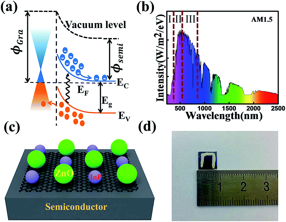 | ||
| Fig. 1 (a) Physical illustration of depletion layer in Gr/semiconductor heterostructure. (b) AM1.5 solar spectrum with obvious minimal values thanks to molecular absorption in Earth's atmosphere. (c) Schematic structure of QDs/Gr/semiconductor. (d) Photograph of a QDs/Gr/GaAs solar cell. | ||
2. Experimental section
2.1. Fabrication of solar cell
Growth of monolayer Gr on copper foils was carried out at 1000 °C for 60 min with reaction source flux ratio of CH4![[thin space (1/6-em)]](https://www.rsc.org/images/entities/char_2009.gif) :H2 equaling to 5:1 by chemical vapor deposition (CVD) technique.30 Then polymethyl methacrylate (PMMA) working as the supporting layer was spun on Gr before removing the copper foil, and PMMA was subsequently removed by acetone for about 10 min. Trilayer Gr was obtained by multi-transferring monolayer Gr. The obtained ZnO and InP QDs were eventually diluted in ethanol and cyclohexane solvent, respectively. Thin film n-doped GaAs with a thickness of 2 μm was grown with metal organic CVD at 400 °C, at the same time, the doping concentration of the GaAs wafer was about 1 × 1018 cm−3. Then rear Au contact with a thickness of 60 nm was thermally evaporated on back surface of GaAs wafer. Native oxide on GaAs was removed by dipping the wafers into 10% wt dilute hydrochloric acid solution for 3 min. Surface passivation of GaAs was achieved by soaking treatment of mixed solution of ammonia sulfide and ammonia for 10 min. Gr was transferred onto the surface of ready GaAs, drying in air for half an hour and annealing for 10 min at 120 °C. Then PMMA at the surface of Gr was removed by acetone and silver paste was pasted onto Gr, followed by 120 °C/5 min post-anneal. Basing on the above operation, Gr/GaAs solar cell preliminarily came into being. Finally, the key manipulation was carried out as follows: InP QDs were spun on Gr at 4000 rpm for 60 s, and then the similar operation was performed again so as to introduce ZnO QDs to the surface of Gr.
:H2 equaling to 5:1 by chemical vapor deposition (CVD) technique.30 Then polymethyl methacrylate (PMMA) working as the supporting layer was spun on Gr before removing the copper foil, and PMMA was subsequently removed by acetone for about 10 min. Trilayer Gr was obtained by multi-transferring monolayer Gr. The obtained ZnO and InP QDs were eventually diluted in ethanol and cyclohexane solvent, respectively. Thin film n-doped GaAs with a thickness of 2 μm was grown with metal organic CVD at 400 °C, at the same time, the doping concentration of the GaAs wafer was about 1 × 1018 cm−3. Then rear Au contact with a thickness of 60 nm was thermally evaporated on back surface of GaAs wafer. Native oxide on GaAs was removed by dipping the wafers into 10% wt dilute hydrochloric acid solution for 3 min. Surface passivation of GaAs was achieved by soaking treatment of mixed solution of ammonia sulfide and ammonia for 10 min. Gr was transferred onto the surface of ready GaAs, drying in air for half an hour and annealing for 10 min at 120 °C. Then PMMA at the surface of Gr was removed by acetone and silver paste was pasted onto Gr, followed by 120 °C/5 min post-anneal. Basing on the above operation, Gr/GaAs solar cell preliminarily came into being. Finally, the key manipulation was carried out as follows: InP QDs were spun on Gr at 4000 rpm for 60 s, and then the similar operation was performed again so as to introduce ZnO QDs to the surface of Gr.
2.2. Characterization
InP and ZnO QDs were transferred to the carbon transmission electron microscopy (TEM) grid for morphology measurement using TEM (Tecnai F-30 operating at 300 kV). Trilayer Gr with and without QDs was characterized by Raman spectroscopy (Renishaw in Via Reflex) with 532 nm excitation source and 0.65 mW laser power. The absorption spectra and photoluminescence (PL) measurements of InP and ZnO QDs in ethanol and cyclohexane solvent were characterized by Cary 4000 of Agilent and FS920 of Edinburgh, respectively. PL measurements used to evaluate the charge transferring behaviors at the interface of Gr/QDs were characterized by a Jobin Yvon HR 640 monochromator with a 325 nm He–Cd laser as the excitation source. The photovoltaic performance of the QDs/Gr/GaAs solar cells was tested with a solar simulator under AM1.5G condition at illumination intensity of 100 mW cm−2. The illumination intensity was calibrated with a standard Si solar cell. The current density–voltage (J–V) data were recorded using Agilent B1500A system.3. Results and discussion
InP and ZnO QDs are transferred to carbon grid for TEM characterizations to reveal the morphology and lattice structure of QDs. Fig. 2 shows TEM images of these two kinds of QDs in different magnifications and their electron diffraction pattern. Fig. 2(a) and (c) show the low-magnification TEM images of InP and ZnO QDs. From the high-magnification TEM images shown in Fig. 2(b) and (d), we can draw a conclusion that these two kinds of QDs possess a high crystal quality and average diameters of InP and ZnO QDs are about 5 nm and 15 nm, respectively. Moreover, the insets show electron diffraction pattern of InP and ZnO QDs, where the diffraction lines can be well labeled by the lattice planes of InP and ZnO. Trilayer Gr for Raman measurements is transferred to SiO2/Si substrate by wet transferring process, which is then coated with InP and ZnO QDs step by step. The corresponding Raman spectra of Gr are shown in Fig. 3(a). For as-grown Gr, there are three characteristic peaks locating at 1350 cm−1, 1591 cm−1 and 2695 cm−1, corresponding to D, G and 2D peaks, respectively. After spinning these two kinds of QDs on the surface of Gr, the G peak blue-shifts to 1596 cm−1, which indicates that p-doping of Gr is enhanced by coating InP QDs and ZnO QDs subsequently. Fig. 3(b) shows the absorption spectra of ZnO and InP QDs in ethanol and cyclohexane solvent, respectively. For InP QDs, absorbance at short wavelength is very high, while it is very weak at long wavelength, and the absorption peak locates around 485 nm. For ZnO QDs, the absorbance is even weaker than InP QDs and the absorption peak locates around 374 nm of ultraviolet wavelength. Actually, these measurements are consistent with their inherent band gap (Eg) structure. To be specific, InP QDs with an even smaller Eg than ZnO QDs can absorb much more energy of incident light. Moreover, these two different kinds of QDs can absorb photon with different energy and their photo-inducing effect can be accumulated. At the same time, these two kinds of QDs possess weak absorbance in visible wavelength, so GaAs substrate can effectively absorb other available incident light.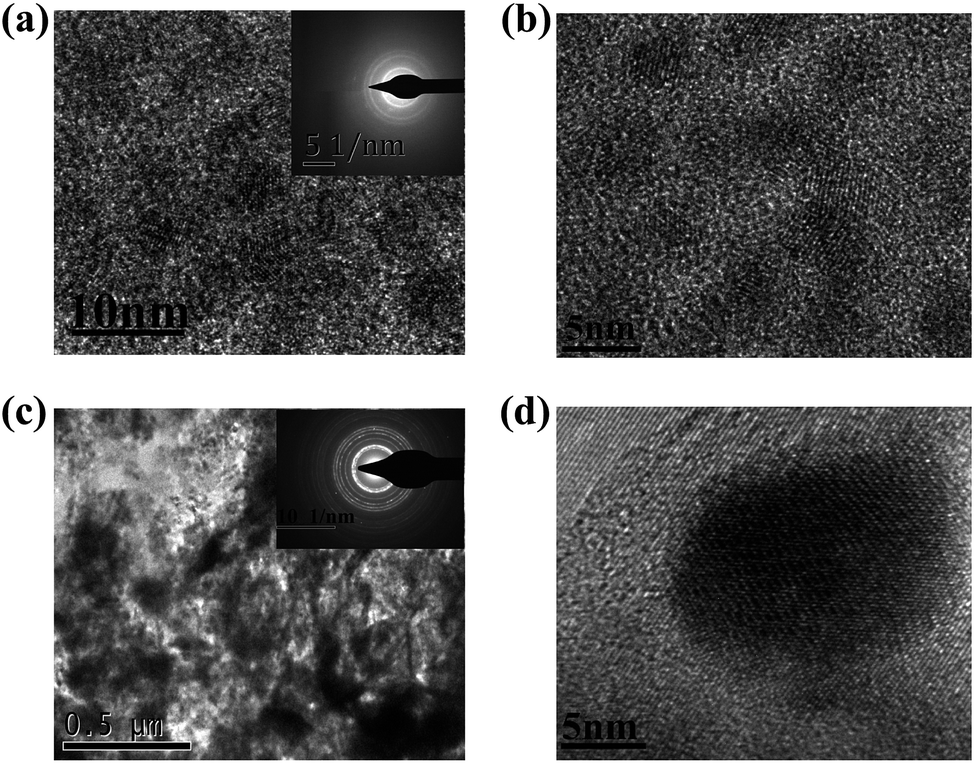 | ||
| Fig. 2 Low-magnification (a) and high-magnification (b) TEM images of the InP QDs. Low-magnification (c) and high-magnification (d) TEM image of the ZnO QDs. Insets show electron diffraction pattern of the InP (a) and ZnO (c) QDs. | ||
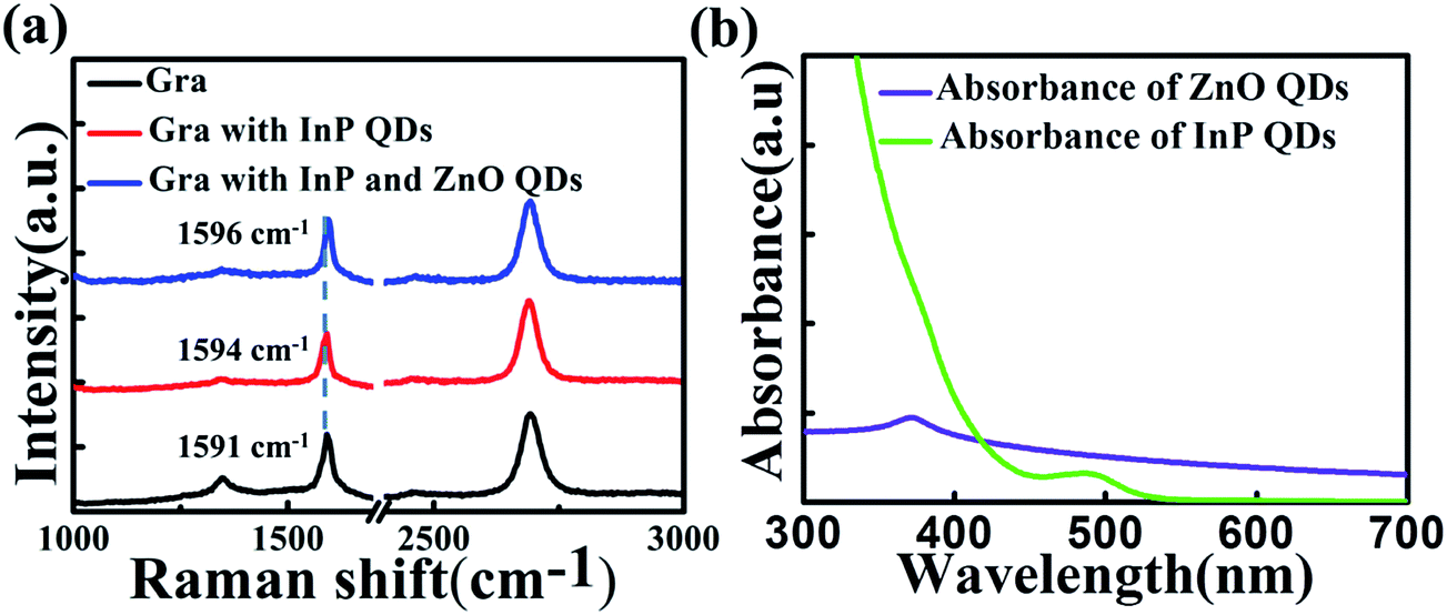 | ||
| Fig. 3 (a) Raman spectra of trilayer Gr without and with QDs underlying on SiO2/Si substrate. (b) Absorption spectra of InP and ZnO QDs in corresponding solvent. | ||
Fig. 4(a) shows the PL spectra of InP and ZnO QDs in ethanol and cyclohexane solvent with the excitation laser line of 405 and 325 nm, respectively. For InP QDs, there is a visible luminescence (VL) band with a maximum at about 515 nm which corresponds to the band-to-band recombination (2.4 eV). For ZnO QDs, PL spectrum mainly contains an ultraviolet luminescence band with a maximum at about 380 nm and a VL band with a maximum at about 510 nm. Indeed, the phenomenon of wide PL band probably attributes to the function of defect levels. Fig. 4(b) illustrates the PL spectra of the InP QDs with 325 nm excitation laser. It is notable that InP QDs are directly spun on SiO2/Si and Gr/SiO2/Si substrate for PL measurements. In vertical direction, the PL intensity of InP QDs is one magnitude larger without Gr underlying than that of the case with Gr underlying, which demonstrates that a majority of laser-induced carriers hop into the Gr. Fig. 4(c) shows the PL spectra of ZnO QDs with 325 nm excitation laser on SiO2/Si and Gr/SiO2/Si substrate. Similar experimental results can be distinctly observed that PL intensity reduces an order of magnitude after coating the QDs on the surface of Gr. Fig. 4(d) schematically illustrates the mechanism of the InP and ZnO QDs introducing photo-induced p-doping into Gr. More concretely, the photo-induced holes from valance band and defect levels hop into Gr, while electrons are trapped in the inner of QDs. Furthermore, the injected holes and negative-charged QDs can greatly influence the carrier concentration in Gr, slightly adjusting the EF-Gr.31
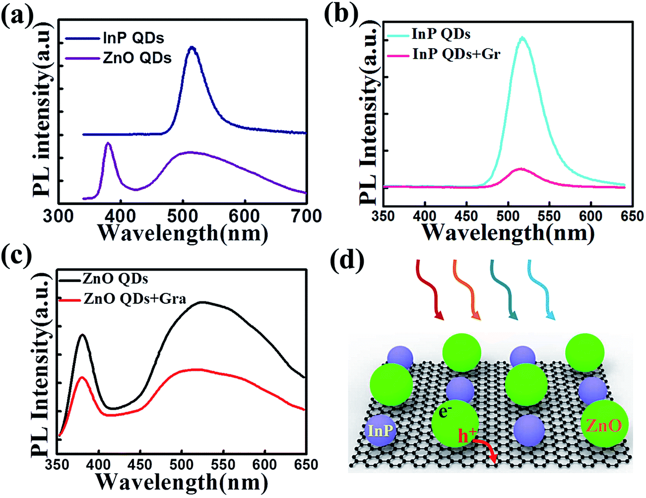 | ||
| Fig. 4 (a) PL spectra of InP and ZnO QDs in solvent. PL spectra of the InP (b) and ZnO (c) QDs with and without Gr underlying on the SiO2/Si substrate using 325 nm He–Cd laser as the excitation source. (d) Physical picture of InP and ZnO QDs generated photo-induced p-doping in Gr. | ||
The schematic structure of enhanced Gr/GaAs heterostructure solar cell with ZnO and InP ODs is shown in Fig. 5(a), which consists of Au gate electrode, n-type GaAs substrate, trilayer Gr, Ag contact, ZnO and InP QDs. InP and ZnO QDs solution are dropped onto the surface of Gr/GaAs solar cell and gently baked for 3 min. J–V curves of the Gr/GaAs solar cell with and without QDs under AM1.5G illumination are shown in Fig. 5(b). Without any QDs, the best PCE  of device is 8.57% and the corresponding parameters of solar cell containing open circuit voltage (Voc), short circuit current density (Jsc), circuit and fill factor (FF) are 0.67 V, 17.80 mA cm−2, and 71.80%, respectively. After coating the InP QDs on surface of Gr at the front top of solar cell, Jsc is increased to 22.02 mA cm−2, Voc is slightly increased to 0.68 V, but FF is slightly decreased to 69.42%, so the PCE is evidently increased to 10.39%. To our best knowledge, this decreasing trend of FF primarily results from corresponding enhancement of Gr's surface resistance. Then some ZnO QDs are spun on the surface of Gr, Jsc is further increased to 24.41 mA cm−2, resulting in the finial PCE of 11.50%. Therefore, the PCE enhancement resulting from the photo-induced doping is distinct. In Fig. 5(c), J–V curves of the Gr/GaAs solar cells with and without QDs in the dark perform similar rectifying characteristics, from which ideality factor can be obtained through single-diode fitting based on the following eqn (1):
 | (1) |
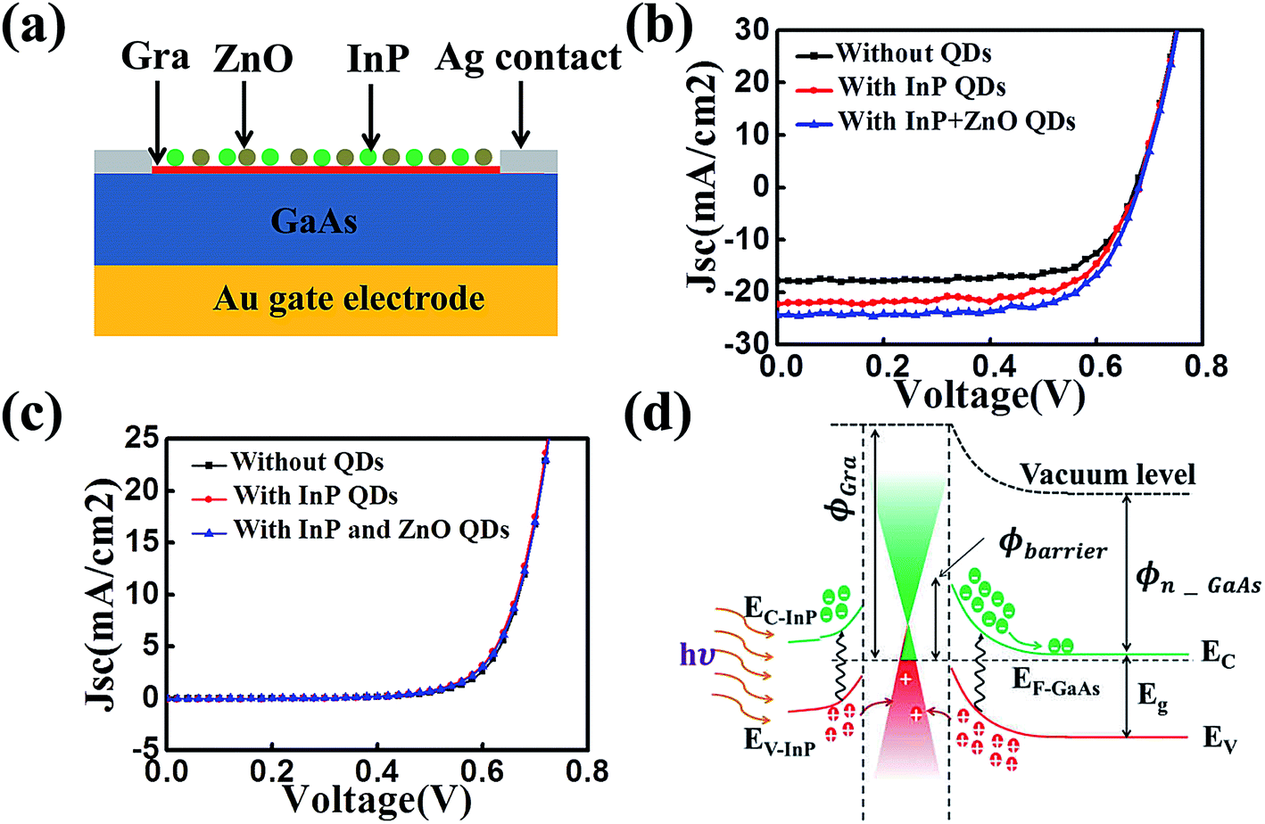 | ||
| Fig. 5 (a) The schematic cross-section view of Gr/GaAs solar cell with two different kinds of semiconductor QDs. Experimental J–V curves under AM1.5G illumination (b) and in the dark of the solar device with and without InP and ZnO QDs (c). (d) Physical picture of electronic band structure of InP and ZnO QDs coating on Gr/GaAs heterostructure solar cell. | ||
Based on thermionic-emission theory, saturation current density J0 can be described as eqn (2):
 | (2) |
Eventually, stability and repeatability of DQs/Gr/GaAs solar cell are well investigated. Statistical analysis of PCE is operated by ten samples of QDs/Gr/GaAs solar cells. Specifically, the PCE distribution of each of the ten samples of Gr/GaAs and QDs/Gr/GaAs solar cells is illustrated in Fig. 6(a) where the result of obviously enhanced PCE of solar cells can easily be observed after introducing QDs, fully illustrating the practicability of photo-induced doping of Gr/GaAs solar cells. Furthermore, two samples of solar cells with QDs under sunlight illumination for 10 days are randomly used for investigation of stability. As shown in Fig. 6(b), PCE degradation is as low as 0.61% for these solar cells, indicating photo-induced doping Gr/GaAs solar cell with good stability can be sustained operation.
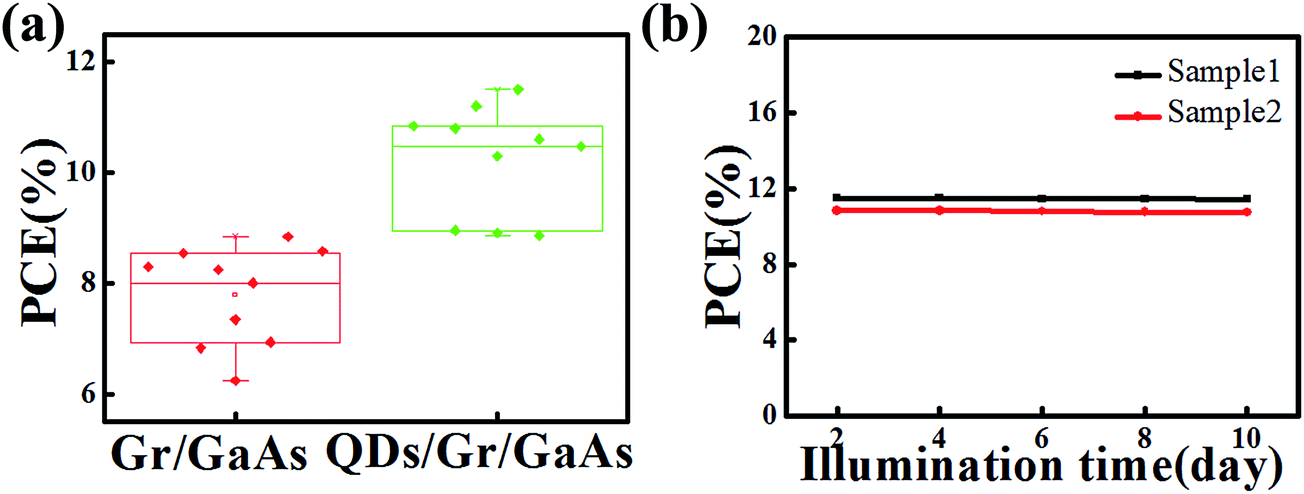 | ||
| Fig. 6 (a) PCE distribution of the Gr/GaAs and QDs/Gr/GaAs solar cells. (b) Stability of the QDs/Gr/GaAs solar cells under AM1.5G illumination. | ||
4. Conclusion
In conclusion, an ingenious approach to obtain the even higher PCE of Gr/GaAs by making full use of solar energy has been proposed. Two kinds of semiconductor QDs, InP and ZnO QDs, are applied to improve the performance of Gr/GaAs solar cell by photo-induced holes doping of Gr. To be specific, the PCE of Gr/GaAs can be increased from original 8.57% to 11.50% after spinning InP and ZnO QDs step by step. Therefore, under this cooperative photo-induced doping, the final PCE is improved by 34.2%. Good stability of QDs/Gr/GaAs solar cell is also fully confirmed. Further work may be necessary to explore the relation between the different combinations of various QDs that can absorb photon with different energy. Overall, this paper provides an easy and feasible way to develop promising Gr/semiconductor heterostructure devices for photovoltaic and optoelectronic applications.Acknowledgements
S. S. Lin thanks the support from the National Natural Science Foundation of China (No. 51202216, No. 51551203 and No. 51502264), Special Foundation of Young Professor of Zhejiang University (No. 2013QNA5007).Notes and references
- W. Liao, D. Zhao, Y. Yu, C. R. Grice, C. Wang, A. J. Cimaroli, P. Schulz, W. Meng, K. Zhu, R.-G. Xiong and Y. Yan, Adv. Mater., 2016, 28, 9333–9340 CrossRef CAS PubMed.
- L. M. Pazos-Outón, M. Szumilo, R. Lamboll, J. M. Richter, M. Crespo-Quesada, M. Abdi-Jalebi, H. J. Beeson, M. Vrućinić, M. Alsari, H. J. Snaith, B. Ehrler, R. H. Friend and F. Deschler, Science, 2016, 351, 1430–1433 CrossRef PubMed.
- M. Saliba, T. Matsui, K. Domanski, J.-Y. Seo, A. Ummadisingu, S. M. Zakeeruddin, J.-P. Correa-Baena, W. R. Tress, A. Abate, A. Hagfeldt and M. Grätzel, Science, 2016, 354, 206–209 CrossRef CAS PubMed.
- F. De Nicola, M. Salvato, C. Cirillo, M. Crivellari, M. Boscardin, M. Scarselli, F. Nanni, I. Cacciotti, M. D. Crescenzi and P. Castrucci, Carbon, 2016, 101, 226–234 CrossRef CAS.
- K. P. Loh, S. W. Tong and J. S. Wu, J. Am. Chem. Soc., 2016, 138, 1095–1102 CrossRef CAS PubMed.
- T. Salim, H. W. Lee, L. H. Wong, J. H. Oh, Z. A. Bao and Y. M. Lam, Adv. Funct. Mater., 2016, 26, 51–65 CrossRef CAS.
- K. H. Hendriks, A. S. G. Wijpkema, J. J. van Franeker, M. M. Wienk and R. A. J. Janssen, J. Am. Chem. Soc., 2016, 138, 10026–10031 CrossRef CAS PubMed.
- Y. Guo, Y. Li, O. Awartani, J. Zhao, H. Han, H. Ade, D. Zhao and H. Yan, Adv. Mater., 2016, 28, 8483–8489 CrossRef CAS PubMed.
- C. Z. Li, J. Huang, H. X. Ju, Y. Zang, J. Y. Zhang, J. F. Zhu, H. Z. Chen and A. K. Y. Jen, Adv. Mater., 2016, 28, 7269–7275 CrossRef CAS PubMed.
- D. P. McMeekin, G. Sadoughi, W. Rehman, G. E. Eperon, M. Saliba, M. T. Hörantner, A. Haghighirad, N. Sakai, L. Korte, B. Rech, M. B. Johnston, L. M. Herz and H. J. Snaith, Science, 2016, 351, 151–155 CrossRef CAS PubMed.
- K. A. Bush, C. D. Bailie, Y. Chen, A. R. Bowring, W. Wang, W. Ma, T. Leijtens, F. Moghadam and M. D. McGehee, Adv. Mater., 2016, 28, 3937–3943 CrossRef CAS PubMed.
- J. Liu, S. Lu, L. Zhu, X. Li and W. C. H. Choy, Nanoscale, 2016, 8, 3638–3646 RSC.
- X. Q. Li, S. S. Lin, X. Lin, Z. J. Xu, P. Wang, S. J. Zhang, H. K. Zhong, W. L. Xu, Z. Q. Wu and W. Fang, Opt. Express, 2016, 24, 134–145 CrossRef CAS PubMed.
- A. K. Geim, Science, 2009, 324, 1530–1534 CrossRef CAS PubMed.
- R. R. Nair, P. Blake, A. N. Grigorenko, K. S. Novoselov, T. J. Booth, T. Stauber, N. M. R. Peres and A. K. Geim, Science, 2008, 320, 1308 CrossRef CAS PubMed.
- S. Chen, Z. Han, M. M. Elahi, K. M. M. Habib, L. Wang, B. Wen, Y. Gao, T. Taniguchi, K. Watanabe, J. Hone, A. W. Ghosh and C. R. Dean, Science, 2016, 353, 1522–1525 CrossRef CAS PubMed.
- K. S. Novoselov, Z. Jiang, Y. Zhang, S. V. Morozov, H. L. Stormer, U. Zeitler, J. C. Maan, G. S. Boebinger, P. Kim and A. K. Geim, Science, 2007, 315, 1379 CrossRef CAS PubMed.
- A. A. Balandin, S. Ghosh, W. Z. Bao, I. Calizo, D. Teweldebrhan, F. Miao and C. N. Lau, Nano Lett., 2008, 8, 902–907 CrossRef CAS PubMed.
- C. Lee, X. D. Wei, J. W. Kysar and J. Hone, Science, 2008, 321, 385–388 CrossRef CAS PubMed.
- S. J. Zhang, S. S. Lin, X. Q. Li, X. Y. Liu, H. A. Wu, W. L. Xu, P. Wang, Z. Q. Wu, H. K. Zhong and Z. J. Xu, Nanoscale, 2016, 8, 226–232 RSC.
- X. L. Zhang, C. Hagglund and E. M. J. Johansson, Adv. Funct. Mater., 2016, 26, 1253–1260 CrossRef CAS.
- X. Q. Li, W. C. Chen, S. J. Zhang, Z. Q. Wu, P. Wang, Z. J. Xu, H. S. Chen, W. Y. Yin, H. K. Zhong and S. S. Lin, Nano Energy, 2015, 16, 310–319 CrossRef CAS.
- D. L. Boyda, V. V. Braguta, S. N. Valgushev, M. I. Polikarpov and M. V. Ulybyshev, Phys. Rev. B: Condens. Matter Mater. Phys., 2014, 89, 6 CrossRef.
- D. M. Forrester and F. V. Kusmartsev, Nanoscale, 2014, 6, 7594–7603 RSC.
- P. H. Cheng, L. G. Wu, X. Li, T. Li, H. X. Zhao and J. L. Bao, Opt. Commun., 2015, 335, 279–283 CrossRef CAS.
- S. S. Lin, Z. Q. Wu, X. Q. Li, Y. J. Zhang, S. J. Zhang, R. Panneerselvam and J. F. Li, Adv. Energy Mater., 2016, 6, 5 Search PubMed.
- S. S. Lin, X. Q. Li, S. J. Zhang, P. Wang, Z. J. Xu, H. K. Zhong, Z. Q. Wu and H. S. Chen, Appl. Phys. Lett., 2015, 107, 5 Search PubMed.
- P. Wang, S. S. Lin, G. Q. Ding, X. Q. Li, Z. Q. Wu, S. J. Zhang, Z. J. Xu, S. Xu, Y. H. Lu, W. L. Xu and Z. Y. Zheng, Appl. Phys. Lett., 2016, 108, 4 Search PubMed.
- N. Petrone, C. R. Dean, I. Meric, A. M. van der Zande, P. Y. Huang, L. Wang, D. Muller, K. L. Shepard and J. Hone, Nano Lett., 2012, 12, 2751–2756 CrossRef CAS PubMed.
- X. S. Li, W. W. Cai, J. H. An, S. Kim, J. Nah, D. X. Yang, R. Piner, A. Velamakanni, I. Jung, E. Tutuc, S. K. Banerjee, L. Colombo and R. S. Ruoff, Science, 2009, 324, 1312–1314 CrossRef CAS PubMed.
- G. Konstantatos, M. Badioli, L. Gaudreau, J. Osmond, M. Bernechea, F. P. G. de Arquer, F. Gatti and F. H. L. Koppens, Nat. Nanotechnol., 2012, 7, 363–368 CrossRef CAS PubMed.
- M. S. Carpenter, M. R. Melloch, M. S. Lundstrom and S. P. Tobin, Appl. Phys. Lett., 1988, 52, 2157–2159 CrossRef CAS.
- W. J. Jie, F. G. Zheng and J. H. Hao, Appl. Phys. Lett., 2013, 103, 4 CrossRef.
- S. Sarkar, E. Bekyarova and R. C. Haddon, Acc. Chem. Res., 2012, 45, 673–682 CrossRef CAS PubMed.
| This journal is © The Royal Society of Chemistry 2017 |