
 Open Access Article
 This Open Access Article is licensed under a Creative Commons Attribution-Non Commercial 3.0 Unported Licence
Patterning Bi2Se3 single-crystalline thin films on Si(111) substrates using strong oxidizing acids
Lei Gao ac,
Handong Li*a,
Wuyang Renb,
Gaoyun Wanga,
Hui Lia,
Zhihua Zhoua,
Haining Jia,
Xiaobin Niua and
Zhiming Wangb
ac,
Handong Li*a,
Wuyang Renb,
Gaoyun Wanga,
Hui Lia,
Zhihua Zhoua,
Haining Jia,
Xiaobin Niua and
Zhiming Wangb
aState Key Laboratory of Electronic Thin Films and Integrated Devices, School of Microelectronics and Solid-State Electronics, University of Electronic Science and Technology of China, Chengdu 610054, China. E-mail: hdli@uestc.edu.cn
bInstitute of Fundamental and Frontier Sciences, University of Electronic Science and Technology of China, Chengdu 610054, China
cMicrosystem and Terahertz Research Center, Chinese Academy of Engineering Physics, Chengdu 610200, China
First published on 23rd June 2017
Abstract
Acidic potassium dichromate solutions (K2Cr2O7–H2SO4 and K2Cr2O7–HCl) are applied for patterning single crystalline Bi2Se3 thin films on Si(111) substrates. In solutions with appropriate component proportions, vertical walls and mesa-shaped structures on the etching profiles of (001) Bi2Se3 films can be achieved. Stoichiometric etching behavior is noted for Bi2Se3 in K2Cr2O7–H2SO4 etchant, while incongruently dissolution of Bi2Se3 in K2Cr2O7–HCl is observed which leaves a Se deficient layer on the etched film surface. The chemical reaction kinetics of Bi2Se3 in the two different etchants are also discussed.
1. Introduction
The layered compound Bi2Se3 has been used for thermoelectric (TE) energy conversion for years.1,2 After being revealed as a topological insulator (TI), Bi2Se3 has become much more sought-after than ever before.3 Featuring a large bulk band gap (∼0.3 eV) and simple Dirac-cone shaped surface states, Bi2Se3 is advocated as the most promising TI for room temperature applications.4,5 Some fingerprints of Bi2Se3 TI surface states have already been detected in electronic transport measurements, such as B–A interference effects,6 anti-localization behaviors,7 and unique anisotropic magneto-resistance.8 These findings have promised novel quantum devices of Bi2Se3 beyond its traditional TE applications. Furthermore, high quality Bi2Se3 thin films can be readily grown on substrates such as Si,9–11 GaAs,12 and InP13,14 at rather low temperatures (∼500 K), which sensibly promotes bottom-up on-chip integration of Bi2Se3 devices.However, as a key step towards device realization, patterning Bi2Se3 thin films is still of challenge. Physical bombardment of argon ions and reactive ion etching offer very little selectivity of the sample material over photoresist and carbonization of photoresist masks due to long term exposure to high energy ion beams may ensue. The complicated operation also hinders the popularity of dry-etch in processing weakly-bonded Bi2Se3. As compared to dry etching approaches, wet etching is an effective alternative due to its high etching rate, low cost and high selectivity. The etchants with different etching velocity, surface roughness, and some other characteristics can further be worked out for various purpose. Among etchants ever employed for Bi2Se3 and other chalcogenides, iodine and/or bromine based chemistries promise selective surface etching at limited rate.15 For fast chemical cutting of bismuth chalcogenides, the most popular wet etchant ever used is aqueous solutions of HNO3 and HCl mixture (diluted aqua regia).16–21 However, these highly corrosive solutions could cause a vigorous uncontrollable reaction with Bi2Se3, resulting in severe edge undercutting. The diluted aqua regia etchants become even detrimental for handling thin films because they either cause pattern disappearance or trigger the delamination of weakly adhering Bi2Se3 films from bottom substrates.22
In this work, oxidizing etchants based on K2Cr2O7–H2SO4 and K2Cr2O7–HCl solutions are used for patterning Bi2Se3 thin film electrodes on Si, respectively. K2Cr2O7–H2SO4–HCl ternary system has been verified suitable for using in etching solutions of covalent GaAs and InP wafers before.23 It's demonstrated that the simpler K2Cr2O7–H2SO4 and K2Cr2O7–HCl binary aqueous solutions can also produce mesa-shaped structures with vertical walls of layered Bi2Se3 thin films in this research. Superior surface morphologies of the etched Bi2Se3 (001) over the un-etched ones are obtained in solutions with proper acidities. However, incongruently etching behaviors on the Bi2Se3 surfaces are noted that a Se depletion surface layer is formed on Bi2Se3 etched in the K2Cr2O7–HCl solutions.
2. Experimental section
Single crystalline Bi2Se3 thin films grown on (111)-oriented Si substrates by physical vapor deposition are adopted in this study. Details of thin film growth can be found in our previously published work.11 The thickness of Bi2Se3 films involved in this study is ∼300 nm. Photoresist etching mask is made by standard photolithography. About 1 μm thick resist (AZ5214) is masked on each Bi2Se3 film surface by spin coating. After being prebaked for 65 seconds at 100 degree, the samples are exposed to ultraviolet light for 20 seconds. Submicron ultraviolet mask aligner is applied in this step. After removing the unexposed photoresist in developer solution and rinsed in deionized water, patterned samples are obtained. To enhance the adhesion of photoresist, all the samples are post baked for 5 minutes at 110 degree.The K2Cr2O7–HCl (H2SO4) etchants are prepared by intermixing 9 v/v% K2Cr2O7 and 48 v/v% HCl (98 v/v% H2SO4) solutions in volume proportions of 1![[thin space (1/6-em)]](https://www.rsc.org/images/entities/char_2009.gif) :1, 1:2, and 1:3 (thereafter denoted by 1:n K2Cr2O7–HCl (H2SO4), n = 1, 2, 3), respectively at room temperature. As in Table 1, the acquired acidities, as represent by H+ concentration ([H+]) in the solutions, are calculated to be 6 mol L−1, 8 mol L−1, and 9 mol L−1 for the 1:1, 1:2, and 1:3 K2Cr2O7–HCl etchants, respectively. For the 1:1 to 1:3 K2Cr2O7–H2SO4 etchants, [H+] values are 9 mol L−1, 12 mol L−1, and 13.5 mol L−1, respectively. The Bi2Se3 films are etched in these aqueous acidic solutions for given time and no stirring is carried out to isolate the influence from hydromechanical effect. After etching, the samples are rinsed in acetone until the photoresist can be stripped. To investigate the dissolution of Bi2Se3, ascertain the character of corresponding reactions and determine limiting stages of the process, various methods are involved in the experiments. The thickness of the etched films is measured by a surface profilometer (Dektak150, Veeco). Optical microscopy (Olympus BX51), atomic force microscopy (AFM), and scanning electron microscopy (SEM) are employed to investigate the surface morphologies of the obtained patterns. Surface structural and compositional details of etched samples are further studied by Raman and electron dispersive spectroscopy (EDX), respectively. The chemical identification and binding energy study of the etched Bi2Se3 films are conducted by X-Ray Photoelectron Spectroscopy (XPS, Omicron).
:1, 1:2, and 1:3 (thereafter denoted by 1:n K2Cr2O7–HCl (H2SO4), n = 1, 2, 3), respectively at room temperature. As in Table 1, the acquired acidities, as represent by H+ concentration ([H+]) in the solutions, are calculated to be 6 mol L−1, 8 mol L−1, and 9 mol L−1 for the 1:1, 1:2, and 1:3 K2Cr2O7–HCl etchants, respectively. For the 1:1 to 1:3 K2Cr2O7–H2SO4 etchants, [H+] values are 9 mol L−1, 12 mol L−1, and 13.5 mol L−1, respectively. The Bi2Se3 films are etched in these aqueous acidic solutions for given time and no stirring is carried out to isolate the influence from hydromechanical effect. After etching, the samples are rinsed in acetone until the photoresist can be stripped. To investigate the dissolution of Bi2Se3, ascertain the character of corresponding reactions and determine limiting stages of the process, various methods are involved in the experiments. The thickness of the etched films is measured by a surface profilometer (Dektak150, Veeco). Optical microscopy (Olympus BX51), atomic force microscopy (AFM), and scanning electron microscopy (SEM) are employed to investigate the surface morphologies of the obtained patterns. Surface structural and compositional details of etched samples are further studied by Raman and electron dispersive spectroscopy (EDX), respectively. The chemical identification and binding energy study of the etched Bi2Se3 films are conducted by X-Ray Photoelectron Spectroscopy (XPS, Omicron).
| Etch solution | Proportion | [H+] (mol L−1) |
|---|---|---|
| K2Cr2O7–HCl | 1:1 |
6 |
| K2Cr2O7–HCl | 1:2 |
8 |
| K2Cr2O7–HCl | 1:3 |
9 |
| K2Cr2O7–H2SO4 | 1:1 |
9 |
| K2Cr2O7–H2SO4 | 1:2 |
12 |
| K2Cr2O7–H2SO4 | 1:3 |
13.5 |
3. Results and discussion
Fig. 1(a) shows a photograph of a Bi2Se3 film etched by using 1:2 K2Cr2O7–HCl solution. A grid pattern of Bi2Se3 with designed 8 μm line width and 50 × 50 μm2 windows is left on the Si substrate after thoroughly etching. Fig. 1(b) exhibits Raman curves taken from the Bi2Se3 grid and the etched window area of the sample, respectively. Three strong peaks locating at 71 cm−1, 131 cm−1 and 173 cm−1 are attributed to the A11g, E2g, and A21g transitions of pure Bi2Se3 respectively,24,25 which indicates a good crystallinity of the un-etched part of Bi2Se3 film. While there are only two peaks of Si(111) (299.4 cm−1 and 520 cm−1) found on the Raman spectrum from the etched area, indicating a complete removal of Bi2Se3 without any deposits left on the Si substrate after chemical reaction. A cross-sectional SEM image of the etched Bi2Se3 pattern further manifests the details at the edge of the etched Bi2Se3 film. As shown in Fig. 1(c), the side wall of the etched groove is straight and perpendicular to the horizontal surface of Bi2Se3 film which unambiguously depicts the superiority of the acid K2Cr2O7 solution in obtaining mesa-shape microstructures of Bi2Se3.
 | ||
| Fig. 1 (a) An optical photograph of a 1:2 K2Cr2O7–HCl solution etched Bi2Se3 film with rectangular grid pattern. (b) Raman curves taken from the grid line (red) and window region (black) on (a), respectively. (c) Cross-sectional SEM image indicates the side-wall structure of the etched Bi2Se3 film in (a). | ||
For better describing the dissolving properties of Bi2Se3 in acid K2Cr2O7 solutions, the etching depths (θ) of the Bi2Se3 film are measured at different time intervals (t). A typical θ–t curve of Bi2Se3 in 1:2 K2Cr2O7–HCl etchant is shown in Fig. 2(a), and a constant etching rate of ∼120 nm min−1 is calculated from its linear fitting, indicating a rate-controlled etching reaction. It must be pointed out that the etching almost ceases at depth of 350 nm which is possibly due to the consumption of [H+] in the solution. Also noted from the θ–t curve is the reaction delay of Bi2Se3 during the initial 15 seconds before the balanced etching rate can be reached. Such behavior is also observed in all other reactions. By carefully excluding any extrinsic contamination on sample surfaces, we suppose the initial dissolving of Bi2Se3 is hindered by a thick native oxidized layer formed on each sample surface which has suffered long-time exposure in air. The induction period varies a lot for different Bi2Se3 samples, despite of the same acidity and temperature conditions are adopted in those reactions, which is ascribed to the reaction dependence on different chemical compositions and/or thicknesses of the oxidized layers on Bi2Se3 samples, and would not be discussed here. After the induction period, the reaction accelerates and the dissolving process of Bi2Se3 exhibits clear dependence on both the reaction temperatures and acidities of the etchants. Fig. 2(b) shows the quantitative Bi2Se3 etching rate dependence on acidities of K2Cr2O7–HCl and temperatures (20 °C to 45 °C). In the [H+]: 6 mol L−1 etchant, the chemical reaction is weak that rather slight dissolution of the film can be detected even after the solution temperature is elevated from 20 °C to 45 °C (actually, the etching rate is only increased from 10 nm min−1 to a few tens of nanometers per minute as temperature ramps up from 20 °C to 45 °C). While after the [H+] of the K2Cr2O7 etchants is increased larger than 8 mol L−1, the chemical reaction is obviously activated and the etching rates yield rapid increase at elevated temperatures. As judged from the measured rate curves depicted in Fig. 2(b), the dissolution of Bi2Se3 in 1:3 K2Cr2O7–HCl is nearly three times faster than it in 1:2 K2Cr2O7–HCl etchant at room temperature. To quantitatively describe the chemical reaction intensity of Bi2Se3 in the oxidizing acids with different [H+], we calculate the activation energies of etching reactions of Bi2Se3 in 1:1, 1:2, and 1:3 K2Cr2O7–HCl solutions (the corresponding [H+] is 6 mol L−1, 8 mol L−1, and 9 mol L−1, respectively) from the plots using Arrhenius equation for these curves shown in Fig. 2(b), and the calculated activation energies are 0.88 eV, 0.74 eV, and 0.47 eV, respectively. It thus strongly manifests that the chemical reaction barrier of Bi2Se3 in the oxidizing acids decreases dramatically as the acidity increases in the etching solutions. However, such an intense reaction leads to severely uneven etching of the patterned film. As shown in inset of Fig. 2(b) is an optical microscopic picture of slightly etched Bi2Se3 by 1:3 K2Cr2O7–HCl solution at room temperature, on which it can be clearly figured out that the areas near the grid corners are attacked much faster than the other regions. As the etching proceeds, undesired “W”-shape depth profiles of the film gradually evolve and part of the Bi2Se3 grid pattern gets eventually dissolved.
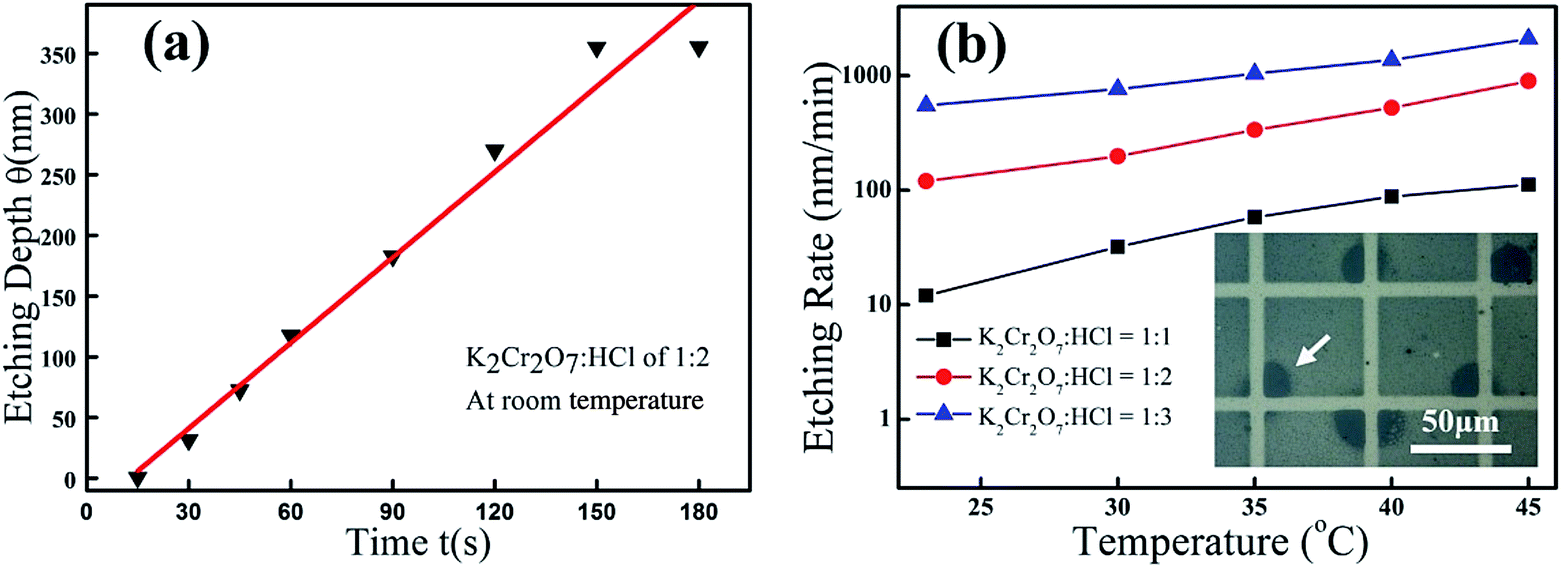 | ||
| Fig. 2 (a) Time-dependent etching depth evolution of Bi2Se3 in 1:2 K2Cr2O7–HCl solution. (b) Temperature-dependent etching rates of Bi2Se3 in 1:1, 1:2, and 1:3 K2Cr2O7–HCl solutions, respectively. Inset in (b) is a typical optical microscopic picture taken from a Bi2Se3 film with square grid pattern immersed in 1:3 K2Cr2O7–HCl for 5 seconds. The arrow indicates an over-eroded site on the pattern. | ||
Almost the same etching behaviors of Bi2Se3 in K2Cr2O7–H2SO4 etchants are observed. The 1:2 in K2Cr2O7–H2SO4 ([H+]: 12 mol L−1) etchant also yields the same etching rate of ∼120 nm min−1 as obtained in the 1:2 in K2Cr2O7–HCl and can produce “U” shape etching profiles of the Bi2Se3 films. Anyway, the electronic characteristics of electrodes and heterojunctions based on the etched Bi2Se3 subject on the microscopic surface properties, it's therefore necessary to analyze the morphologies and stoichiometry of the Bi2Se3 surfaces etched by these two kinds of etchants. As illustrated in Fig. 3(a) is a SEM image of an as-deposited Bi2Se3 thin film. High dense growth spirals surrounded by straight steps are observed in the as-grown Bi2Se3 thin films (highlighted by dashed triangles in Fig. 3(a)). As measured by AFM, the root mean square (RMS) roughness of such surface is ∼3 nm (in area of 5 × 5 μm2), as shown in Table 2. After being immersed in 1:2 K2Cr2O7–H2SO4 solution for 30 seconds which corresponds to an etching depth of ∼60 nm, these pyramid morphologies completely vanish and a surface decorated with large amounts of irregular-shaped islands sized from ∼20 nm to ∼300 nm comes out as exhibited in Fig. 3(b). The surface morphology does not improve too much (RMS roughness ∼2.5 nm) as compared to the as-deposited Bi2Se3 film. On such etched surface, a Se:Bi mole ratio of ∼1.60 is detected by EDX measurement. The Se:Bi mole ratio doesn't change significantly after a further 30 seconds etching period indicates a stoichiometric dissolution of Bi2Se3 in the 1:2 in K2Cr2O7–H2SO4 etchant. Fig. 3(c) shows a SEM image taken from a Bi2Se3 film etched in 1:2 in K2Cr2O7–HCl solution at ∼60 nm depth too. A much smoother surface (RMS roughness ∼1.5 nm) is obtained for Bi2Se3 in this etchant. Not identical to the case of Bi2Se3 in 1:2 in K2Cr2O7–H2SO4, Se:Bi mole ratio on the 1:2 in K2Cr2O7–HCl etched surface is ∼1.1 as measured by EDX, implying a Se-dissolving preferred reaction kinetics. As etching proceeds to ∼270 nm depth, only Bi signal from the film can be detected by EDX indicating a full depletion of Se. It should be noted that the good epitaxial character with two-dimensional surface terrace-step structures of initial Bi2Se3 films disappears after being etched in both solutions, which strongly implies that both etching processes would cause amorphous surface parts of the Bi2Se3 films. It's thus also reasonable to attribute the nano-sized islands with irregular shapes (as shown in Fig. 3(b) and (c)) to be amorphous Bi2Se3 deposits after etching.
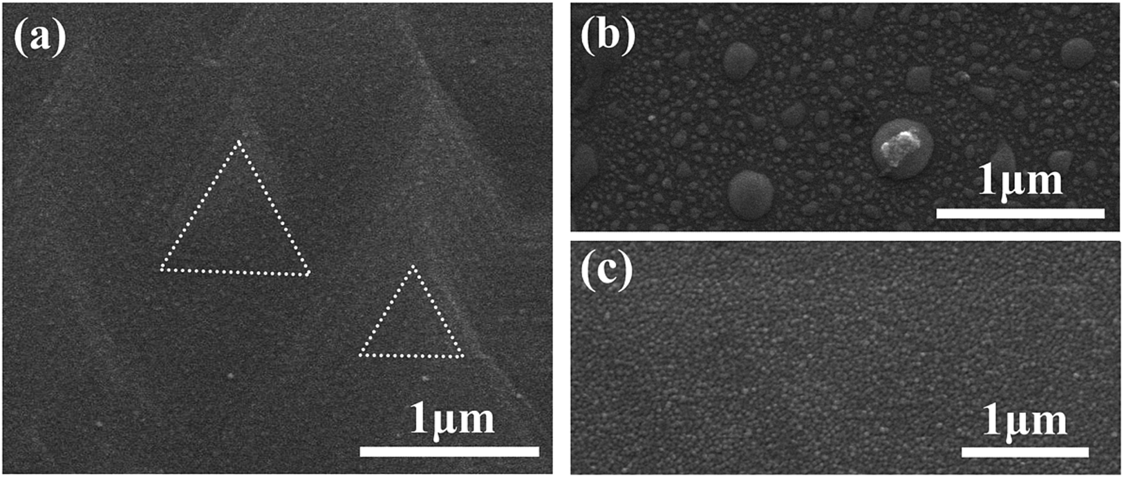 | ||
| Fig. 3 SEM images of an as-deposited Bi2Se3 surface (a) and Bi2Se3 surfaces etched in 1:2 K2Cr2O7–H2SO4 etchant (b) and 1:2 K2Cr2O7–HCl etchant (c), respectively. | ||
:Bi mole ratio before and after etched by 1:2 K2Cr2O7–HCl (H2SO4) etchants
| Sample surface | RMS roughness | Se:Bi mole ratio |
|---|---|---|
| Un-etched Bi2Se3 thin film | 3 nm | 1.6 |
| In 1:2 K2Cr2O7–H2SO4 solution for 30 s |
2.5 nm | 1.6 |
| In 1:2 K2Cr2O7–HCl solution for 30 s |
1.5 nm | 1.1 |
It's well known that wet chemical etching proceeds by oxidation of the semiconductor constituents followed by chemical dissolution of the oxides in suitable solvents. For etching covalent chalcogenides such as CdSe, CdTe, and HgCdTe, different dissolving rates between cations and chalcogens are often observed because the hydration of cations is much easier than that of nonfully-oxidized chalcogens on the material surfaces.26–29 As a result, the etched surfaces of chalcogenides are usually cation-deficient. While no cation-deficient surfaces of etched Bi2Se3 are obtained in our experiments, which suggests quite different reaction kinetics of layered Bi2Se3 as compared to that of covalent chalcogenides in oxidizing acids etchants. To further understand the chemical reaction kinetics of Bi2Se3 in oxidizing acids with different components, XPS study is carried out for characterizing the chemical status of Bi2Se3 surfaces etched in different acid K2Cr2O7 solutions.
As shown in Fig. 4 are core level spectrum of Bi and Se elements detected by XPS from the samples etched in 1:2 K2Cr2O7–HCl and 1:2 K2Cr2O7–H2SO4 etchants with etching depth of ∼60 nm, respectively. The binding energies (BE) obtained in the XPS analysis are standardized for specimen charging using C 1s peak as the reference at 284.8 eV. To precisely determine the peaks' positions, Lorentz–Gauss profiles and Shirley background have been taken for the deconvolution. As indicated in Fig. 4(a) is Bi 4f spectrum from the K2Cr2O7–H2SO4 etched Bi2Se3 sample, in which the intensity contribution for spin–orbit-splitting Bi 4f peaks (4f7/2 and 4f5/2) from either Bi–O bonding30,31 or Bi–Se bonding can be clearly distinguished upon deconvolution. The intensities of Bi–O bonding Bi peaks are much stronger than that of Bi–Se bonding Bi peaks, which suggest there exists a bismuth oxide (BiOx) thin layer deposited on the Bi2Se3 surface during etching. While for the K2Cr2O7–HCl etched Bi2Se3 case, only a pair of Bi 4f peaks located at 158.82 eV and 164.11 eV are observed which can be precisely attributed to Bi–Se bonding of pure Bi2Se3 (Fig. 4(b)).32–34 Peaks referred to Se 3p1/2 and Se 3p3/2 can also be figured out in both fitted XPS spectra as exhibited in Fig. 4(a) and (b), and the broaden peak profiles depict a mixed valence states of Se on both samples.35 The valence states of Se from Bi2Se3 films after etched by K2Cr2O7–H2SO4 and K2Cr2O7–HCl are further investigated by analyzing the peak fitted Se 3d (3d5/2 and 3d3/2) spectra as illustrated in Fig. 4(c) and (d), respectively. In either Se 3d curve, the pair of high BE component peaks belong to Se–Se bonding of element Se and the other pair are related to Bi–Se bonding, respectively. And no traces of any selenium oxides can be found on the etched Bi2Se3 surfaces in our XPS studies.30 Therefore, it's reasonable to determine that there's only a Se2− → Se0 oxidizing reaction happens for the Se element in both etching processes and the free element Se reactants are deposited onto the Bi2Se3 surfaces. Further, peak intensity contribution from Se–Se bonding dominates in Se 3d spectra of the K2Cr2O7–H2SO4 etched Bi2Se3 sample while it becomes not prominent in K2Cr2O7–HCl etched one, which manifests that there're more Se deposits residual on K2Cr2O7–H2SO4 etched Bi2Se3 surface than those on K2Cr2O7–HCl etched one.
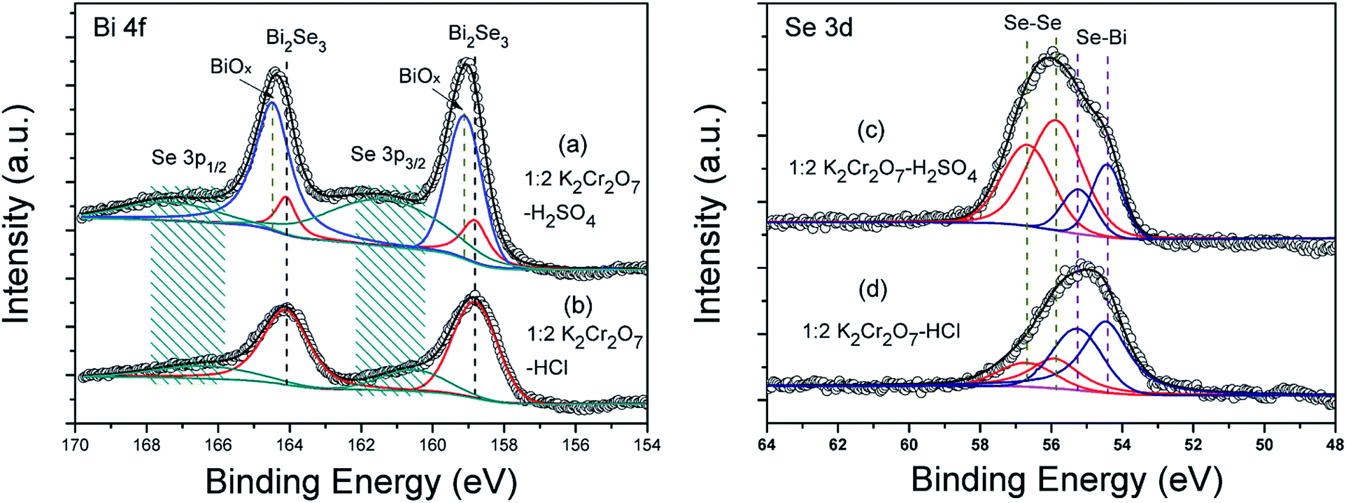 | ||
| Fig. 4 Bi 4f and Se 3d XPS spectra of Bi2Se3 films after etched by 1:2 K2Cr2O7–H2SO4 etchant [(a) and (c)] and by 1:2 K2Cr2O7–HCl etchant [(b) and (d)], respectively. Experimental data are the open circles and fits are the solid lines. | ||
Based on the XPS observations, it should be feasible to determine that the surface chemistry is predominated by bismuth oxides and element Se all through the etching procedure in K2Cr2O7–H2SO4 solutions. Therefore the surface reaction kinetics are only subjected by the rate of reactants reaches and leaves the etched surface.36 As to our knowledge, there's only tempered chemical reactions happen between bismuth oxides and concentrated acids (such as H2SO4 and HCl) at room temperature. So do them between element Se and concentrated sulphuric acid. As a result, congruently dissolving of Bi and Se will dominate in the etching reaction which is confirmed by our experiment observations.
On the other hand, the valence states of Bi in Bi2Se3 remains intact during etching in K2Cr2O7–HCl solutions. It's thus suggested that the etching action on the Bi2Se3 surface is fully triggered by dissolving of Se. As a result, it leads to the observed incongruently etching behaviors of Bi2Se3 in K2Cr2O7–HCl etchants.
4. Conclusions
To summary, mesa-shaped etching profile of Bi2Se3 is obtained either in 1:2 K2Cr2O7–HCl or 1:2 K2Cr2O7–H2SO4 aqueous solutions with H+ concentrations of 8 mol L−1 and 12 mol L−1, respectively. Dissolving rates of Bi2Se3 are approximately 120 nm min−1 in both the 1:2 K2Cr2O7–H2SO4 and 1:2 K2Cr2O7–HCl etchants at room temperature. Though either etchant is qualified for preparing desired microscopic patterns of Bi2Se3, quite distinct dissolving kinetics between these two etchants significantly lead to different reaction products on surfaces of the etched samples. In 1:2 K2Cr2O7–H2SO4 etching case, the surface stoichiometry of Bi2Se3 is found intact that the TI surface states would probably being reserved after etching. While the Se-deficient dissolving behavior of Bi2Se3 noted in the K2Cr2O7–HCl etchants implies surface quality degradation. Nevertheless, slightly metal-rich surface may benefit a low-resistance ohmic contact formation between Bi2Se3 and electrode metals that has been argued crucial for improving performance of TE devices.37 Considering chemical treatment of semiconductor surfaces is a convenient way to define the surface properties and manufacture micropatterns, our findings may serve as useful reference for fabricating Bi2Se3-based devices with various purpose.
Acknowledgements
This work is supported by the National Natural Science Foundation of China (Grant No. 11104010, 61474014, 51272038, and 51302030) and Open Research Fund Program of the State Key Laboratory of Low-Dimentional Quantum Physics (No. 20120910).References
- C. Wood, Rep. Prog. Phys., 1988, 51, 459–539 CrossRef CAS.
- G. Chen, M. S. Dresselhaus, G. Dresselhaus, J. P. Fleurial and T. Caillat, Int. Mater. Rev., 2003, 48, 45–66 CrossRef CAS.
- D. Hsieh, Y. Xia, D. Qian, L. Wray, F. Meier, J. H. Dil, J. Osterwalder, L. Patthey, A. V. Fedorov, H. Lin, A. Bansil, D. Grauer, Y. S. Hor, R. J. Cava and M. Z. Hasan, Phys. Rev. Lett., 2009, 103, 4 CrossRef PubMed.
- Y. Xia, D. Qian, D. Hsieh, L. Wray, A. Pal, H. Lin, A. Bansil, D. Grauer, Y. S. Hor, R. J. Cava and M. Z. Hasan, Nat. Phys., 2009, 5, 398–402 CrossRef CAS.
- H. Zhang, C. X. Liu, X. L. Qi, X. Dai, Z. Fang and S. C. Zhang, Nat. Phys., 2009, 5, 438–442 CrossRef CAS.
- H. L. Peng, K. J. Lai, D. S. Kong, S. Meister, Y. L. Chen, X. L. Qi, S. C. Zhang, Z. X. Shen and Y. Cui, Nat. Mater., 2010, 9, 225–229 CAS.
- J. Chen, H. J. Qin, F. Yang, J. Liu, T. Guan, F. M. Qu, G. H. Zhang, J. R. Shi, X. C. Xie, C. L. Yang, K. H. Wu, Y. Q. Li and L. Lu, Phys. Rev. Lett., 2010, 105, 4 Search PubMed.
- J. Wang, H. Li, C. Chang, K. He, J. S. Lee, H. Lu, Y. Sun, X. Ma, N. Samarth and S. Shen, Nano Res., 2011, 5, 739–746 CrossRef.
- G. H. Zhang, H. J. Qin, J. Teng, J. D. Guo, Q. L. Guo, X. Dai, Z. Fang and K. H. Wu, Appl. Phys. Lett., 2009, 95, 3 Search PubMed.
- H. D. Li, Z. Y. Wang, X. Kan, X. Guo, H. T. He, Z. Wang, J. N. Wang, T. L. Wong, N. Wang and M. H. Xie, New J. Phys., 2010, 12, 11 Search PubMed.
- H. D. Li, L. Gao, H. Li, G. Y. Wang, J. Wu, Z. H. Zhou and Z. M. Wang, Appl. Phys. Lett., 2013, 102, 4 Search PubMed.
- A. Richardella, D. M. Zhang, J. S. Lee, A. Koser, D. W. Rench, A. L. Yeats, B. B. Buckley, D. D. Awschalom and N. Samarth, Appl. Phys. Lett., 2010, 97, 3 CrossRef.
- X. Guo, Z. J. Xu, H. C. Liu, B. Zhao, X. Q. Dai, H. T. He, J. N. Wang, H. J. Liu, W. K. Ho and M. H. Xie, Appl. Phys. Lett., 2013, 102, 4 Search PubMed.
- S. Schreyeck, N. V. Tarakina, G. Karczewski, C. Schumacher, T. Borzenko, C. Brune, H. Buhmann, C. Gould, K. Brunner and L. W. Molenkamp, Appl. Phys. Lett., 2013, 102, 4 CrossRef.
- S. Augustine and E. Mathai, Mater. Res. Bull., 2001, 36, 2251–2261 CrossRef CAS.
- C. Shafai and M. J. Brett, J. Vac. Sci. Technol., A, 1997, 15, 2798–2801 CAS.
- L. M. Goncalves, J. G. Rocha, C. Couto, P. Alpuim, G. Min, D. M. Rowe and J. H. Correia, J. Micromech. Microeng., 2007, 17, S168–S173 CrossRef CAS.
- L. M. Goncalves, C. Couto, P. Alpuim and J. H. Correia, J. Micromech. Microeng., 2008, 18, 1171–1185 CrossRef.
- J. P. Carmo, L. M. Goncalves and J. H. Correia, IEEE Trans. Ind. Electron., 2010, 57, 861–867 CrossRef.
- L. M. Goncalves, P. Alpuim and J. H. Correia, J. Electron. Mater., 2010, 39, 1516–1521 CrossRef CAS.
- J. P. Carmo, M. F. Silva, J. F. Ribeiro, R. F. Wolffenbuttel, P. Alpuim, J. G. Rocha, L. M. Goncalves and J. H. Correia, Microsyst. Technol., 2011, 17, 1283–1291 CrossRef CAS.
- T. Ngai and U. Ghoshal, Wet etching of Bi2Te3 thin films compatible with microelectronic fabrication processes, 26th International Conference on Thermoelectrics, Jeju, Korea, June 2007 Search PubMed.
- S. Adachi, H. Kawaguchi and G. Iwane, J. Mater. Sci., 1981, 16, 2449–2456 CrossRef CAS.
- J. Zhang, Z. P. Peng, A. Soni, Y. Y. Zhao, Y. Xiong, B. Peng, J. B. Wang, M. S. Dresselhaus and Q. H. Xiong, Nano Lett., 2011, 11, 2407–2414 CrossRef CAS PubMed.
- K. M. F. Shahil, M. Z. Hossain, V. Goyal and A. A. Balandin, J. Appl. Phys., 2012, 111, 8 CrossRef.
- R. Tenne and G. Hodes, Appl. Phys. Lett., 1980, 37, 428–430 CrossRef CAS.
- W. H. Chang, T. Lee and W. M. Lau, J. Appl. Phys., 1990, 68, 4816–4819 CrossRef CAS.
- I. M. Kotina, L. M. Tukhkonen, G. V. Patsekina, A. V. Shchukarev and G. M. Gusinskii, Semicond. Sci. Technol., 1998, 13, 890–894 CrossRef CAS.
- V. Srivastav, R. Pal and H. P. Vyas, Opto-Electron. Rev., 2005, 13, 197–211 CAS.
- D. Kong, J. J. Cha, K. Lai, H. Peng, J. G. Analytis, S. Meister, Y. Chen, H. J. Zhang, I. R. Fisher and Z. X. Shen, ACS Nano, 2011, 5, 4698–4703 CrossRef CAS PubMed.
- A. J. Green, S. Dey, Y. Q. An, B. O'Brien, S. J. O'Mullane, B. Thiel and A. C. Diebold, 2016, arXiv: cond-mat.mtrl-sci/1601.04057.
- V. V. Atuchin, V. A. Golyashov, K. A. Kokh, I. V. Korolkov, A. S. Kozhukhov, V. N. Kruchinin, S. V. Makarenko, L. D. Pokrovsky, I. P. Prosvirin, K. N. Romanyuk and O. E. Tereshchenko, Cryst. Growth Des., 2011, 11, 5507–5514 CAS.
- M. T. Edmonds, J. T. Hellerstedt, A. Tadich, A. Schenk, K. M. O'Donnell, J. Tosado, N. P. Butch, P. Syers, J. Paglione and M. S. Fuhrer, J. Phys. Chem. C, 2014, 118, 20413–20419 CAS.
- C. Han, J. Yang, C. Yan, Y. Li, F. Y. Liu, L. X. Jiang, J. C. Ye and Y. X. Liu, CrystEngComm, 2014, 16, 2823–2834 RSC.
- V. A. Golyashov, K. A. Kokh, S. V. Makarenko, K. N. Romanyuk, I. P. Prosvirin, A. V. Kalinkin, O. E. Tereshchenko, A. S. Kozhukhov, D. V. Sheglov, S. V. Eremeev, S. D. Borisova and E. V. Chulkov, J. Appl. Phys., 2012, 112, 4 CrossRef.
- Y. C. Lin, Y. C. Jian and J. H. Jiang, Appl. Surf. Sci., 2008, 254, 2671–2677 CrossRef CAS.
- M. Hines, J. Lenhardt, M. Lu, L. Jiang and Z. Xiao, J. Vac. Sci. Technol., A, 2012, 30, 041509 Search PubMed.
| This journal is © The Royal Society of Chemistry 2017 |