
 Open Access Article
 This Open Access Article is licensed under a
 Creative Commons Attribution 3.0 Unported Licence
High-temperature solid-state reaction induced structure modifications and associated photoactivity and gas-sensing performance of binary oxide one-dimensional composite system
Yuan-Chang Liang * and
Ya-Ju Lo
* and
Ya-Ju Lo
Institute of Materials Engineering, National Taiwan Ocean University, Keelung 20224, Taiwan. E-mail: yuanvictory@gmail.com
First published on 6th June 2017
Abstract
The effects of high-temperature solid-state reactions on the microstructures, optical properties, photoactivity, and low-concentration NO2 gas-sensing sensitivity of ZnO–SnO2 core–shell nanorods were investigated. In this study, the ZnO–SnO2 core–shell nanorods were synthesized through a combination of the hydrothermal method and vacuum sputtering. According to X-ray diffraction and transmission electron microscopy analyses, high-temperature solid-state reactions between the SnO2 shell and ZnO core materials at 900 °C engendered an ultrathin SnO2 shell layer for transforming into the ternary Zn2SnO4 (ZTO) phase. Moreover, surface roughening was involved in the high-temperature solid-state reactions, as determined from electron microscopy images. Comparatively, the ZnO–ZTO nanorods have a higher oxygen vacancy density near the nanostructure surfaces than do the ZnO–SnO2 nanorods. The photodegradation of rhodamine B dyes under simulated solar light irradiation in presence of the ZnO–SnO2 and ZnO–ZTO nanorods revealed that the ZnO–ZTO nanorods have a higher photocatalytic activity than do the ZnO–SnO2 nanorods. Furthermore, the ZnO–ZTO nanorods exhibited higher gas-sensing sensitivity than did the ZnO–SnO2 nanorods on exposure to low-concentration NO2 gases. The substantial differences in the microstructure and optical properties between the ZnO–SnO2 and ZnO–ZTO nanorods accounted for the photocatalytic activity and NO2 gas-sensing results obtained in this study.
Introduction
The synthesis of low-dimensional metal oxide composites is a promising approach for designing oxide materials with improved functionalities. Several studies have demonstrated that low-dimensional metal oxide composites have superior photocatalytic activity and gas-sensing performance compared with single-constituent compounds. The photocatalytic activity and gas-sensing sensitivity of metal oxide composites are closely related to their different chemical components, architectures, and microstructures. Various material systems such as Ag2O-decorated flower-like ZnO composites, TiO2–WOx composite tubes, ZnO–ZnFe2O4 composite nanorods, one-dimensional (1D) SnO2–CeO2 composites, and ZnO–In2O3 composite nanorods have been successfully synthesized, and studies have demonstrated that improved photocatalytic activity or gas-sensing sensitivity are highly correlated with the formation of heterojunctions and the resultant microstructural changes in the construction of low-dimensional composites.1–5Among various low-dimensional oxide composites, 1D core–shell oxide composites are one of the most promising heterostructure types that are applied to photocatalysts and gas-sensing fields, with enhanced properties in comparison with their constituent compounds. In general, a formation of low-dimensional oxide composites with satisfactory photocatalytic activity and gas-sensing properties should consider factors related to synthesis methodology and microstructure change. Most 1D oxide composites have been developed through a two-step technique, which might involve a combination of two chemical synthesis methods, either chemical and physical synthesis methods or two physical methods. The chemical durability and stability of the constituent compounds during the various synthesis methods are important for synthesizing various desired 1D composites. The hydrothermal method is promising for facile synthesis of various 1D oxides with a large-area coverage on different types of substrates, easy tailoring of morphology, and easy process parameter control; the hydrothermally derived 1D oxides are useful as templates for growing other oxide materials onto their surfaces to form a core–shell structure.6 Subsequently, the formation of a shell layer occurs through the deposition of an ultrathin layer (tens of nanometer) onto the surfaces of the host material structure. Chemical solution process-related methods, such as sol–gel and dip-coating methods, limit the control of the shell layer thickness, and a subsequent thermal process is usually needed to crystallize the shell layer. By contrast, a sputtering technique allows for any desired shell thickness to be applied simply by controlling the deposition duration, and crystalline shell oxides with controllable microstructures can be obtained through in situ crystal growth at various growing temperatures.7 Because of the different chemical natures of the constituent components, synthesizing the 1D core–shell composites through a combination of hydrothermal and physical synthesis methods is advantageous.5 This synthesis methodology prohibits possible deterioration of the host material crystallite feature during the second step of the chemical solution synthesis process for the shell layer.
Regarding the photocatalytic activity, the surface microstructures of 1D core–shell composites are important to the overall charge collection efficiency, because they can influence the photoexcited charge recombination and the chemical reaction dynamics.8 Furthermore, the gas-sensing sensitivity of 1D core–shell composites is also significantly affected by the surface structure of the shell layer. The heterojunction created at the interface of 1D core–shell composites plays an important role in enhancing the photocatalytic activity and gas-sensing properties when the shell layer thickness is down to tens of nanometers.9,10 Therefore, understanding the modifications in the surface microstructure-dependent photocatalytic activity and gas-sensing properties of 1D oxide core–shell composites is important for designing such composites with satisfactory performances. SnO2 and ZnO are two of the most important metal oxides and are widely used in photocatalysts and gas-sensing materials.11,12 Recent research and enhancement have led to the development of the ternary compound Zn2SnO4 (ZTO), which is based on an integrated composition of ZnO and SnO2. This ternary semiconductor compound is a promising material for application in photocatalysts and gas sensors.13,14 Due to the similar band alignment feature of the ZnO–SnO2 and ZnO–ZTO heterostructures,15,16 these two types of heterostructures are suitable targets for investigating and understanding the physical mechanisms of shell-layer microstructural modifications in the photocatalytic activity and gas-sensing sensitivity of 1D core–shell composites.
In the present study, hydrothermally derived 1D ZnO nanorods were sputtering coated with an ultrathin SnO2 layer to form 1D ZnO–SnO2 core–shell nanorods; moreover, a high-temperature postannealing procedure was conducted to induce a high-temperature solid-state reaction between the ZnO core and SnO2 shell, resulting in the formation of ZnO–ZTO core-sell nanorods. The effects of microstructural and phase modifications on the photocatalytic activity and low-concentration NO2 gas-sensing sensitivity of the ZnO-based composite nanorods were investigated and discussed in this study.
Experiments
In this study, ZnO-based core–shell composite nanorods with the SnO2 and Zn2SnO4 (ZTO) shell layers (ZnO–SnO2 and ZnO–ZTO nanorods) were synthesized through a combinational methodology of hydrothermal and sputtering. Hydrothermally synthesized high-density ZnO nanorods were used as templates for growing the ZnO–SnO2 and ZnO–ZTO composite rods. The hydrothermal growth reactions of the ZnO rods were conducted at 95 °C for 9 hours. The detailed preparation procedures for the hydrothermal growth of the ZnO nanorods have been reported elsewhere.17 During growth of the SnO2 shell layers onto the surfaces of the ZnO rods, the DC sputtering power of Sn metallic target was fixed at 30 W. The thin-film growth temperature was maintained at 325 °C with an Ar/O2 ratio of 25![[thin space (1/6-em)]](https://www.rsc.org/images/entities/char_2009.gif) :15. The gas pressure during sputtering thin-film deposition was fixed at 2.67 Pa. For preparation of ZnO–ZTO composite nanorods, the as-synthesized ZnO–SnO2 core–shell nanorods were subsequently annealed in ambient air for 1 hour at the high temperature of 900 °C to induce a high-temperature solid-state reaction between the ZnO core and SnO2 shell and formed the ZnO–ZTO core–sell nanorods.
:15. The gas pressure during sputtering thin-film deposition was fixed at 2.67 Pa. For preparation of ZnO–ZTO composite nanorods, the as-synthesized ZnO–SnO2 core–shell nanorods were subsequently annealed in ambient air for 1 hour at the high temperature of 900 °C to induce a high-temperature solid-state reaction between the ZnO core and SnO2 shell and formed the ZnO–ZTO core–sell nanorods.
The surface morphology of the nanorod samples was investigated by scanning electron microscopy (SEM; Hitachi S-4800). Sample crystal structures were investigated by X-ray diffraction (XRD; Bruker D2 PHASER) using Cu Kα radiation. The microstructures of the rod samples were characterized by high-resolution transmission electron microscopy (HRTEM; Philips Tecnai F20 G2). X-ray photoelectron spectroscope (XPS; PHI 5000 VersaProbe) analysis was performed to determine the chemical binding states of the constituent elements of the nanostructures. The optical absorption spectra of the samples were recorded in the wavelength range of 300–800 nm by using UV-Vis spectrophotometer (Jasco V750). Room temperature dependent photoluminescence (PL; Horiba HR800) spectra were obtained using the 325 nm line of a He–Cd laser. Photocatalytic activity of various nanorod samples were performed by comparing the degradation of aqueous solution of rhodamine B (RhB; 10−6 M) containing various nanorod samples as catalysts under solar light irradiation excited from a 100 W Xe arc lamp. The solution volume of RhB is 10 ml and the nanorods are grown on the 300 nm-thick SiO2/Si substrates with a fixed coverage area of 1.0 cm × 1.0 cm for photodegradation tests. The variation of RhB solution concentration in presence of various nanorod samples with different irradiation durations was analyzed by recording the absorbance spectra using an UV-Vis spectrophotometer. Silver glues were laid on the surfaces of the nanorods to form two contact electrodes for gas-sensing measurements. To measure oxidizing gas sensing properties, sensors were placed in a closed vacuum chamber and various concentrations (1.0, 2.5, 5.0, 7.5 and 10.0 ppm) of NO2 gas were introduced into the chamber, using dry N2 as the carrier gas. All the sensing properties of the sensors were measured at 300 °C. The gas sensing response of the sensors to NO2 gas is defined as the Rg/Ra. Ra is the electrical resistance of the sensor in the absence of target gas and Rg is the electrical resistance of the sensor in target gas. The response time is defined as the durations required to reach 90% variation in sensor resistance upon exposure to NO2 and the recovery time is the durations required to reach 90% variation in sensor resistance on removal of NO2 gas.12
Results and discussion
Fig. 1(a) shows the top view of a SEM image of the as-synthesized ZnO nanorods. The cross-section of the ZnO nanorods has a hexagonal crystal feature. The SEM image of the ZnO nanorods that were sputtering coated with the SnO2 shell layer is exhibited in Fig. 1(b). Tiny granular crystallites were observed to cover the surfaces of the ZnO nanorods after encapsulating the SnO2 layer through sputtering. The surface became more rugged than that of the ZnO nanorods. The favorable free-standing and rod-like crystal feature of the ZnO was maintained after the thin-film deposition of the SnO2 thin layer. Further postannealing of the ZnO–SnO2 composite nanorods at a high temperature engendered the surface roughening of the composite nanorods (Fig. 1(c)). The surface crystallite size became large when the ZnO–SnO2 composite nanorods were postannealed at a high temperature. This might be associated with the possible phase transformation or crystal growth of the surface grains during the high-temperature solid-state reaction.18 A similar phenomenon, wherein high-temperature annealing causes the surfaces of the core–shell oxide nanostructures to become irregular and rough, has been observed in the ZnO–TiO2 and Ga2O3–ZnO core–shell nanostructures annealed at a high temperature of 800 °C.19,20 Fig. 1(d)–(f) show the XRD patterns of the as-synthesized ZnO nanorods, ZnO–SnO2 nanorods, and ZnO–SnO2 nanorods annealed at 900 °C. In Fig. 1(d), all the diffraction peaks can be indexed to hexagonal wurtzite structure of ZnO (JCPDS no. 005-0664). The XRD pattern demonstrated a strong Bragg reflection of ZnO (200), revealing that most ZnO nanorod crystals are highly c-axis-oriented. In Fig. 1(e), in addition to the Bragg reflections originated from ZnO, three distinct Bragg reflections located at approximately 26.58°, 37.95° and 51.75° were observed, which can be assigned to the (110), (200), and (211) planes of tetragonal SnO2 (JCPDS no. 021-1250), respectively. The XRD pattern revealed that a well formation of the crystalline ZnO–SnO2 composite nanorods when the ZnO nanorod template was sputtering coated with the SnO2 thin film. Fig. 1(f) shows the XRD pattern of the as-synthesized ZnO–SnO2 nanorods annealed at 900 °C. In addition to the Bragg reflections from the remaining ZnO core, the Bragg reflections in the XRD patterns are associated with the cubic ternary ZTO phase (JCPDS no. 024-1470). Moreover, the Bragg reflections of the SnO2 phase were absent in the XRD pattern, revealing that the SnO2 was fully transformed into the ZTO phase during the high-temperature solid-state reaction with the ZnO core. A successful formation of ternary Zn–Ti–O compound from the solid-state reaction of the constituent binary compounds in a one-dimensional structure has been reported in ZnO–TiO2 system with a temperature higher than 800 °C.18 Moreover, it has been shown that the solid-state reaction between ZnO and SnO2 generate a phase formation of the ternary ZTO when the annealing temperature is higher than 900 °C.21 The XRD results herein demonstrated that the annealing temperature of 900 °C in this study is enough to induce the solid-state reaction between the ZnO core and SnO2 shell of the composite nanorods and the formation of the ZTO shell layer on the residual ZnO core. | ||
| Fig. 1 SEM images of various nanorod samples: (a) ZnO. (b) ZnO–SnO2. (c) ZnO–ZTO. XRD patterns of various nanorod samples: (d) ZnO. (e) ZnO–SnO2. (f) ZnO–ZTO. | ||
Fig. 2(a) shows a low-magnification TEM image of a single ZnO–SnO2 core–shell nanorod. A thin SnO2 layer was homogeneously covered over the surface of the ZnO nanorod. The thickness of the SnO2 shell layer is approximately 15–20 nm. The surface crystallite size is in the range of approximately 4–6 nm. The surface of the SnO2 shell layer exhibited a tiny groove surface feature. Fig. 2(b)–(d) show the HRTEM images of the ZnO–SnO2 core–shell nanorod taken from the different local regions at the ZnO/SnO2 interface. From the HRTEM images, the variation size of the surface undulation from the convex to concave portions of the SnO2 layer is approximately 2–3 nm. The clear lattice fringes in the HRTEM images with an interplanar spacing of approximately 0.33 nm and 0.23 nm corresponded to the {110} and {200} lattice plane of the tetragonal SnO2 structure, respectively. The selected area electron diffraction (SAED) pattern was taken from the multiple composite nanorods in order to obtain the sufficient signals from the ultrathin shell layer and to identify the phase structure of the composite nanorods. Fig. 2(e) depicted a formation of the ZnO–SnO2 heterostructure, which exhibited rings consisted of the sharp, bright spots from the ZnO core and the ultrathin SnO2 shell layer. The energy-dispersive X-ray spectroscopy (EDS) spectra displayed in Fig. 2(f) show that Zn, Sn and O are the main constituent elements of the selected composite nanorod. The local composition distribution of the ZnO–SnO2 composite nanorod was investigated using EDS spectra by line scanning across the nanorod (Fig. 2(g)). The intensity profiles of Zn and Sn across to the nanorod exhibited a sharp Sn compositional distribution in the peripheral region of the composite nanorod and a high Zn compositional distribution in the inner region of the composite nanorod. Fig. 3(a) shows a low-magnification TEM image of a single ZnO–ZTO core–shell nanorod. Comparatively, the surface crystallite size of the ZnO–ZTO nanorod is larger than that of the ZnO–SnO2 nanorod and has a size range of approximately 14–20 nm. The ZnO–ZTO nanorod surface exhibited a distinct rugged surface feature; the surface is rougher than that of the ZnO–SnO2 nanorod. Fig. 3(b)–(d) display the HRTEM images of various interfacial regions of the ZnO–ZTO nanorod. The images clearly show that the surface morphology of the shell layer exhibited an irregular grainy feature. The boundaries between the adjacent ZTO crystallites in the shell layer are clear. The ordered lattice fringes with an interval of approximately 0.30 nm and 0.24 nm corresponded to the {220} and {222} lattice distance of the crystallographic planes of the cubic ZTO, respectively. Fig. 3(e) presents the SAED pattern of multiple composite nanorods. Ring patterns consisted of crystallographic planes originated from two different phases of ZnO and ZTO were observed; moreover, no electron diffraction signal contribution from the SnO2 phase was observed, revealing a well formation of the crystalline ZnO–ZTO heterostructure. The TEM structural analysis revealed that the ultrathin SnO2 shell layer was fully transformed into ZTO phase during the high-temperature solid-state reaction with ZnO core material in this study. The elemental composition of the selected composite rod was evaluated to be Zn, Sn and O elements from the EDS spectra in Fig. 3(f). Line-scan profiles of Zn, Sn, and O elements across the ZnO–ZTO composite nanorod (Fig. 3(g)) clearly show that a well ZTO shell layer homogeneously covered on the ZnO core.
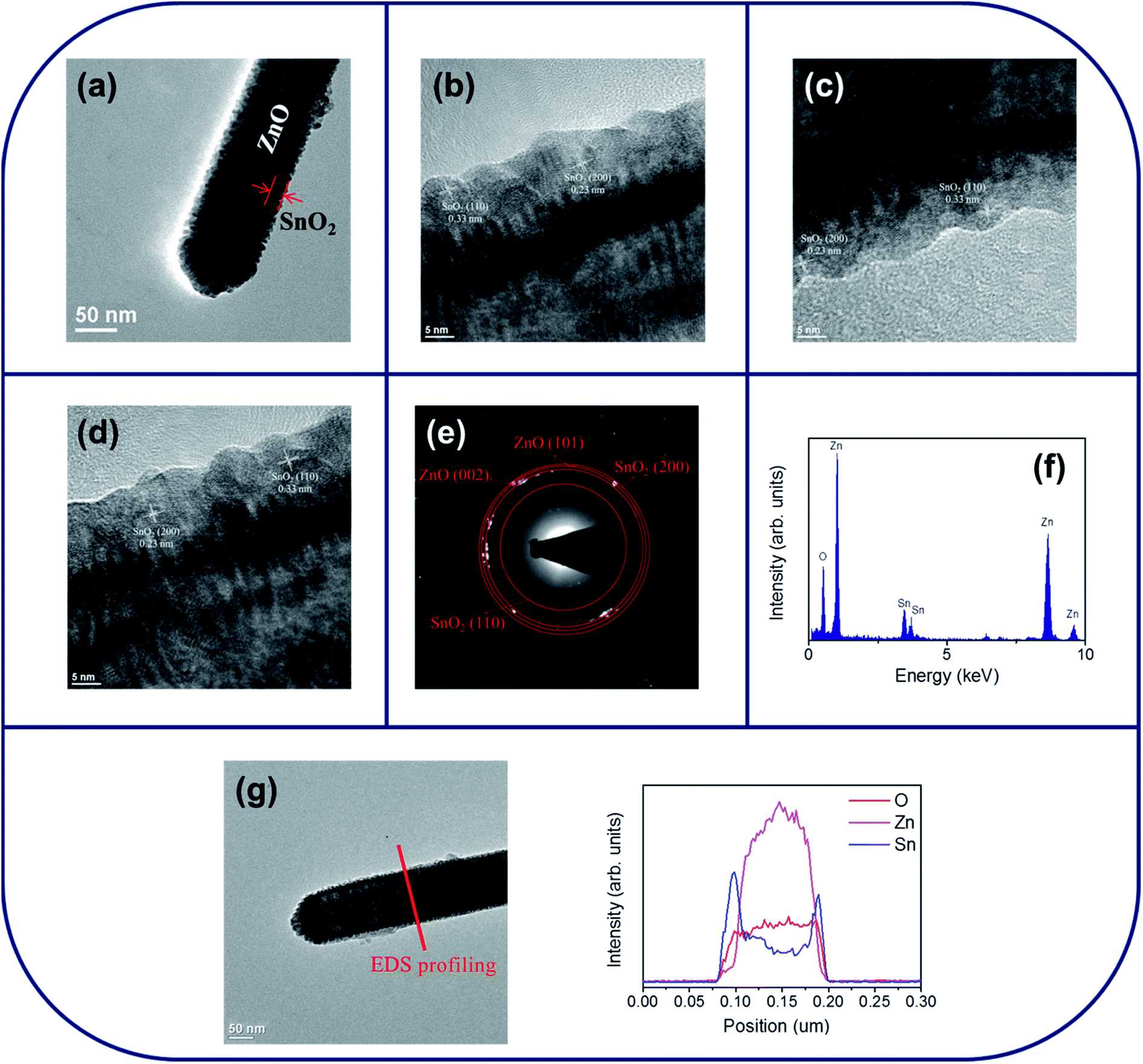 | ||
| Fig. 2 TEM analyses of ZnO–SnO2 nanorod: (a) low-magnification TEM image of the nanorod. (b)–(d) HRTEM images taken from the local regions of the nanorod. (e) SAED pattern taken from the multiple ZnO–SnO2 nanorods. (f) EDS spectra of Zn, Sn, and O elements taken from the nanorod. (g) EDS line-scan profiling spectra across the nanorod. | ||
 | ||
| Fig. 3 TEM analyses of ZnO–ZTO nanorod: (a) low-magnification TEM image of the nanorod. (b)–(d) HRTEM images taken from the local regions of the nanorod. (e) SAED pattern taken from the multiple ZnO–ZTO nanorods. (f) EDS spectra of Zn, Sn, and O elements taken from the nanorod. (g) EDS line-scan profiling spectra across the nanorod. | ||
Fig. 4(a)–(c) show the XPS narrow scan spectra in the Zn 2p region of the ZnO, ZnO–SnO2, and ZnO–ZTO nanorods. The peaks of Zn 2p3/2 for the ZnO, ZnO–SnO2, and ZnO–ZTO nanorods were centered at 1021.7–1022.2 eV; the peaks of Zn 2p1/2 were located at 1044.8–1045.2 eV. The binding energies of the Zn 2p have been ascribed to the binding state of Zn2+ in the ZnO.15,22,23 Fig. 4(d) and (e) show that the symmetric peaks originated from the Sn 3d core-level doublet. The binding energy differences between the Sn 3d3/2 and Sn 3d5/2 peaks for the ZnO–SnO2 and ZnO–ZTO composite nanorods were similar (approximately 8.4 eV), revealing the Sn4+ binding status in the oxides.12,24 No signal from the metallic Sn was observed in the samples, indicating that sputtering deposited the SnO2 thin film, and further postannealing of the ZnO–SnO2 nanorods maintained the Sn4+ in the oxide lattices. Fig. 5(a)–(c) show that the XPS spectra of O 1s for the ZnO, ZnO–SnO2, and ZnO–ZTO nanorods have an asymmetric curve feature. Two Gaussian curves fitted the O 1s peak. The relatively low binding energy component located at approximately 530.1–530.5 eV is associated with the crystal lattice oxygen in the oxide. The high binding energy component located at approximately 531.4–531.9 eV is attributed to the presence of oxygen vacancies within the oxide matrix.25 The peak intensity at the higher binding energy slightly increased when the ZnO nanorods were decorated with the SnO2 shell layer using sputtering. Moreover, the peak intensity at the higher binding energy substantially increased in the ZnO–ZTO nanorods. The relative oxygen vacancy content of the ZnO, ZnO–SnO2, and ZnO–ZTO nanorods was evaluated according to the following intensity ratio of these two Gaussian deconvolution peaks: (red peak)/(red peak + blue peak).26 The relative ratios of oxygen vacancy in the ZnO, ZnO–SnO2, and ZnO–ZTO nanorods were approximately 31%, 37%, and 46%, respectively. The formation of oxygen vacancy in the ZnO nanorods is generally attributed to the high aspect ratio of oxide nanostructures, which easily form oxygen vacancies in the lattices during crystal growth in the low-temperature reaction.27 The slight increase in the oxygen vacancy content of the ZnO–SnO2 nanorods is associated with the fact that the SnO2 thin film was sputtering coated under an oxygen-deficient ambient; this usually causes the formation of oxygen vacancies in the sputtering-deposited oxide thin films.28 Accordingly, the oxygen vacancy content of the composite nanorods substantially increased during the high-temperature solid-state reaction of the ZnO–SnO2 nanorods. The O 1s XPS results revealed that a relatively high degree of oxygen vacancy density was formed in the surfaces of the ZnO–ZTO nanorods.
 | ||
| Fig. 4 XPS narrow scans of Zn 2p region of various nanorod samples: (a) ZnO. (b) ZnO–SnO2. (c) ZnO–ZTO. XPS narrow scans of Sn 3d core level doublet of various nanorod samples: (d) ZnO–SnO2. (e) ZnO–ZTO. | ||
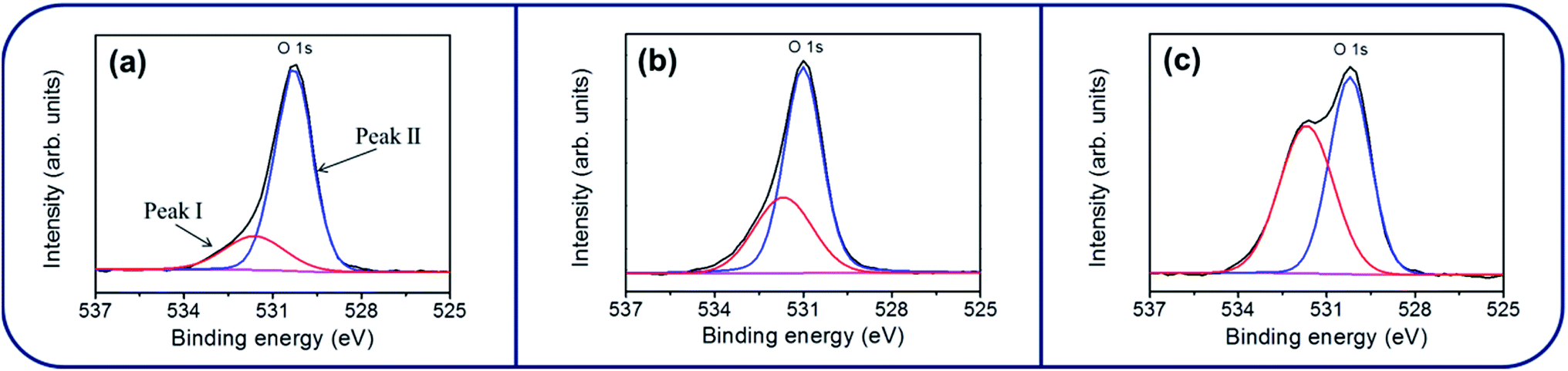 | ||
| Fig. 5 XPS narrow scans of O 1 s core level of various nanorod samples: (a) ZnO. (b) ZnO–SnO2. (c) ZnO–ZTO. | ||
Fig. 6(a) shows the UV-Vis absorbance spectra of the ZnO, ZnO–SnO2, and ZnO–ZTO nanorods. By comparison, a clear redshift was observed for the ZnO nanorods coated with the SnO2 shell layer. Moreover, the ZnO–ZTO nanorods had a larger redshift in comparison with the ZnO–SnO2 nanorods. These results shows that the optical bandgaps of the ZnO-based composite nanorods were narrower than that of the ZnO nanorods when the SnO2 and ZTO were covered onto the surfaces of the ZnO nanorods. The optical bandgaps of the ZnO–SnO2 and ZnO–ZTO nanorods were evaluated according to the formula (F(R)hν)n = C(hν − Eg), where F(R) is the linear absorption coefficient of the material, hν is the photon energy, C is a proportionality constant, and Eg is the bandgap. The exponent n = 2 for direct bandgap semiconductors was used for the oxides herein.29,30 The estimated bandgap values of the ZnO–SnO2 and ZnO–ZTO nanorods are shown in Fig. 6(b). The optical bandgap values of the ZnO–SnO2 and ZnO–ZTO nanorods were approximately 3.17 and 3.11 eV, respectively. Previous studies have reported that a large concentration of oxygen vacancy can induce bandgap narrowing and optical absorbance edge redshift in oxide semiconductors.31,32 Moreover, the wide-bandgap TiO2 and ZnO oxides for forming heterostructures have been shown to engender a clear redshift.33 The composite effects of crystal defects and the shell layer on the ZnO core influenced the optical bandgap of the as-synthesized samples. The effect of high-temperature thermal annealing on the surface defect density of the ZnO–SnO2 composite nanorods was further investigated through PL. Fig. 6(c) illustrates the PL spectra of the ZnO–SnO2 and ZnO–ZTO core–shell nanorods. A sharp and distinct UV emission band was ascribed to the near-band edge (NBE) emission of the ZnO nanorods.22,34 Moreover, a broad and clear visible-light emission band centered at approximately 570 nm was observed for the ZnO–SnO2 and ZnO–ZTO nanorods. This visible emission band was associated with deep-level emissions, which were attributed to the existence of oxygen vacancies near the oxide surface.7 Notably, the NBE intensity of the ZnO–ZTO nanorods decreased significantly compared with that of the ZnO–SnO2 nanorods; moreover, the intensity ratio of the visible emission band to the NBE band was substantially increased when the ZnO–SnO2 nanorods were transformed into the ZnO–ZTO nanorods after high-temperature postannealing. A comparison of the PL spectra between the ZnO–SnO2 and ZnO–ZTO nanorods revealed that an increase in the number of surface crystal defects in the composite nanorods occurs in a high-temperature solid-state reaction. The PL results are consistent with the XPS and UV-Vis analyses, which all supported a higher crystal defect density in the ZnO–ZTO composite nanorods than in the ZnO–SnO2 nanorods.
 | ||
| Fig. 6 (a) Optical absorbance spectra of various nanorod samples. (b) (F(R)hv)2 vs. Photon energy plot. (c) PL spectra of ZnO–SnO2 and ZnO–ZTO nanorods. | ||
The photocatalytic activity of ZnO nanorods with various shell layer materials was compared through photocatalytic decomposition experiments involving RhB dyes. As depicted in Fig. 7(a)–(c), the main absorption peaks of the RhB solution at approximately 550 nm decreased gradually in the presence of the various nanorod photocatalysts under solar light irradiation, with different durations. At a given irradiation duration, the drop in absorbance intensity was more substantial for the RhB solution containing ZnO–ZTO nanorods than that for the solution containing bare-ZnO and ZnO–SnO2 nanorods. The photodegradation degree of the RhB solution for the various nanorod samples was evaluated as C/Co, wherein C is the concentration of RhB remaining in the solution after a given irradiation time, and Co is the initial concentration of RhB without irradiation. The C/Co versus irradiation duration results for various nanorod samples are shown in Fig. 7(d). Dark adsorption tests were performed for various durations before the photocatalytic degradation tests under irradiation. Notably, after 180 min in dark conditions, less than 5% of the RhB dyes were absorbed by the as-synthesized samples in this study. When the adsorption–desorption equilibrium was established, all samples were irradiated with solar light for various durations. From Fig. 7(d), the C/Co values of the ZnO, ZnO–SnO2, and ZnO–ZTO nanorods after 180 min of solar light irradiation were approximately 0.52, 0.36, and 0.17, respectively. The ZnO–ZTO nanorods exhibited a superior photodegradation performance compared with the ZnO and ZnO–SnO2 nanorods. The inset figures show the corresponding times for the RhB solution containing ZnO–SnO2 and ZnO–ZTO nanorods with the photodegradation processes of various durations. Discolorations of the RhB solution containing the ZnO–SnO2 and ZnO–ZTO nanorods under solar light irradiation were visible. Moreover, the RhB solution containing ZnO–ZTO nanorods became almost translucent after 180 min of light irradiation. These observations revealed that the chromophoric structure of the RhB molecules was gradually decomposed during the photodegradation process. Notably, the construction of ZnO–SnO2 and ZnO–ZTO heterostructures enhanced the photodegradation efficiency of the ZnO nanorods. The enhanced photocatalytic ability of the ZnO nanorods toward the RhB dyes, achieved by incorporating SnO2 or the ZTO shell layer, could be detected from the band alignment of the ZnO/SnO2 and ZnO/ZTO (Fig. 8).15,16 Under light irradiation, the electrons (e−) in the valence band are excited to the conduction band, with simultaneous generation of the same amount of holes (h+) in the valance band. Because the conduction band of SnO2 (or ZTO) is lower than that of ZnO, the photoexcited electrons will transfer from the conduction band of ZnO to that of SnO2 (or ZTO). Conversely, the holes transfer from the valance band of SnO2 (or ZTO) to that of ZnO.35 The photogenerated electrons and holes in the as-synthesized nanorod photocatalysts could be injected into a reaction medium and made to participate in degradation reactions with the organic dyes.36 The adsorbed O2 on the shell surfaces of the composite nanorods in the RhB solution can trap the photogenerated electron to produce a superoxide anion radical (˙O2−) (e− + O2 → ˙O2−). The formed ˙O2− reacts with e− and H+ to produce H2O2, which provides a hydroxyl radical (˙OH) by acting as a direct electron acceptor through a reaction with e− and ˙O2−. Moreover, hydroxyl radicals (˙OH) are directly formed by the reaction of the photoexcited holes in the ZnO core with the adsorbed H2O (h+ + H2O →H+ + ˙OH). The hydroxyl radical (˙OH) is an extremely strong oxidant for the mineralization of organic chemicals.37 An efficient charge separation in the ZnO–SnO2 and ZnO–ZTO heterostructures caused by a suitable band alignment between ZnO and SnO2 (or ZTO) decreased the recombination of the photoexcited electron–hole pairs in the composite nanorods. The increased number of free carriers in the composite nanorods substantially contributed to the higher photodegradation performance of the ZnO–SnO2 and ZnO–ZTO nanorods than that of the pure ZnO nanorods under irradiation. An enhanced efficiency in the interfacial charge transfer to adsorbed pollutants has been observed in the SnO2–TiO2 heterostructure system, which has a band alignment feature similar to that of the ZnO–SnO2 and ZnO–ZTO nanorods in this work.38 Additionally, the superior photocatalytic performance of the ZnO–ZTO nanorods compared with that of the ZnO–SnO2 nanorods in this study is associated with microstructural differences between the ZnO–SnO2 and ZnO–ZTO nanorods. PL analysis revealed that the charge separation efficiency of the ZnO–ZTO nanorod was substantially higher than that of the ZnO–SnO2 nanorod. It is posited that the surface crystal defects in semiconductors act as traps and prevent the recombination of photoexcited electrons and holes.39 In WO3 and BiPO4 oxide semiconductors, research results demonstrate that the surface oxygen vacancy of the oxides accelerates the separation of the photoinduced electron–hole pairs and improves the photocatalytic properties accordingly.40,41 Moreover, the ZnO–ZTO nanorods' having a more rugged surface compared with that of the ZnO–SnO2 nanorods increased multiple light scattering between the nanorods and irradiated solar light in the photodegradation tests.5,11 UV-Vis optical analysis results revealed that the ZnO–ZTO nanorod had a higher degree of light-harvesting efficiency under solar light irradiation. The literature has shown that postannealing-induced surface roughening in ZnO–CdS nanorods contributes to enhanced photocatalytic properties because of the improved light harvesting of the ZnO–CdS composite nanorods.42 The aforementioned factors account for the superior photocatalytic activity of the ZnO–ZTO nanorods in this study.
 | ||
| Fig. 7 Intensity variation of absorbance spectra of RhB solution vs. degradation duration containing various nanorod samples under solar light illumination: (a) pure ZnO nanorods. (b) ZnO–SnO2 nanorods. (c) ZnO–ZTO nanorods. (d) C/Co vs. irradiation time curves for RhB solution containing various nanorod samples in dark conditions and under solar light illumination. The pictures of the RhB solution containing ZnO–SnO2 and ZnO–ZTO nanorods under solar light illumination at different durations are displayed for a comparison. | ||
 | ||
| Fig. 8 The schematics of band structure and charges transfer of the (a) ZnO–SnO2 and (b) ZnO–ZTO. | ||
Fig. 9(a)–(c) show the dynamic gas-sensing response curves of the ZnO, ZnO–SnO2, and ZnO–ZTO nanorods to NO2 gas at various concentrations (1–10 ppm). The sensitivity of the sensors made from various nanorods to various NO2 concentrations is summarized in Fig. 9(d). Clearly, the gas-sensing sensitivity of the various sensors increased with the NO2 gas concentration; this is because higher NO2 gas concentrations caused more NO2 gas molecules to adsorb onto the surfaces of the nanorods during the gas-sensing tests. The gas-sensing sensitivities of the gas sensor comprising ZnO nanorods increased from 1.7 to 2.3 when the NO2 gas concentration was increased from 1 to 10 ppm. The gas-sensing sensitivities of the sensor with ZnO–SnO2 nanorods were 4.4 and 9.8 on exposure to 1 and 10 ppm NO2 gas, respectively. At a given NO2 gas concentration, the gas-sensing sensitivities of the sensor comprising ZnO–ZTO nanorods were higher than those of the sensors made from ZnO and ZnO–SnO2 nanorods. The response times of the sensor comprising ZnO nanorods were in the range of approximately 74–118 s, and the recovery times were in the range of 838–1205 s on exposure to 1–10 ppm of NO2 gas. Moreover, the response times of the sensor made from ZnO–SnO2 nanorods were in the range of approximately 62–82 s, and the recovery times were in the range of 692–1069 s on exposure to 1–10 ppm of NO2 gas. For the sensor made from ZnO–ZTO nanorods, the response times and recovery times on exposure to 1–10 ppm of NO2 gas were in the ranges of 56–79 s and 488–907 s, respectively. Comparatively, the formation of a SnO2 shell layer or ZTO shell layer onto the surfaces of the ZnO nanorods markedly decreased the response time and recovery time during the gas-sensing tests. The gas sensor comprising ZnO–ZTO nanorods exhibited superior NO2 gas-sensing performance in this study, achieving the highest gas-sensing sensitivity and shortest response time and recovery time on exposure to NO2 gas at a given NO2 concentration. A schematic diagram (Fig. 10(a)–(c)) was used to explain the differences in gas-sensing response behavior of the ZnO, ZnO–SnO2, and ZnO–ZTO nanorods. First, with respect to ZnO nanorods, the application of the SnO2 and ZTO shell layers to ZnO nanorods produced more active sites on the surfaces of the ZnO–SnO2 and ZnO–ZTO nanorods for adsorbing NO2 gas molecules with higher efficiency (Fig. 10(b) and (c)). This is attributed to the fact that the surfaces of the ZnO–SnO2 and ZnO–ZTO nanorods are more rugged than those of pure ZnO nanorods, which have a smooth surface (Fig. 10(a)). Of various nanorod samples, the ZnO–ZTO nanorods exhibited the roughest surface features, as revealed from the aforementioned microstructural analyses. The surfaces of the ZnO–ZTO are expected to provide more adsorbed sites for the NO2 gas molecules during the gas-sensing tests. The rough surface of TiO2–WO3 nanorods results in an increment in the number of surface-adsorbed oxygen ions, quickens the rate of the sensing reaction between reductive gases and surface-adsorbed oxygen ions, and facilitates the gas adsorption and diffusion on composite nanorods, thus leading to enhanced gas-sensing performance.43 Moreover, oxygen vacancies, which are a commonly observed point defect in n-type oxides, are beneficial for the gas-sensing behavior of n-type semiconductor oxides. Oxygen vacancies donate electrons to the conduction band of n-type semiconductor oxides, and the existence of oxygen vacancies in nanostructured oxide surfaces increases the electrostatic interaction between the oxide surface and the reactive NO2 molecules.44 The high-temperature solid-state reaction formation of the ZTO shell of the ZnO–ZTO nanorods produced more oxygen vacancies in its surface. The ZTO surface had a higher concentration of donor-related defects and higher NO2 gas-molecule surface adsorption efficiency than did the SnO2 shell of the ZnO–SnO2 and ZnO nanorod surfaces. In addition to the microstructural differences among the various nanorod samples, which might affect their NO2 gas-sensing performance, the band alignment between the core and shell materials plays an important role in affecting the gas-sensing performance. Notably, the work function of ZnO is 5.2 eV; SnO2 and ZTO have a similar value of 4.9 eV.15,45 The work function value of ZnO is higher than that of SnO2 and ZTO; accordingly, when the heterostructure was formed, a thin depletion layer was expected to form in the SnO2 and ZTO shell layers and an electron accumulation layer in the ZnO core;46 a marked potential barrier was formed at the heterointerface between the ZnO and SnO2 (or ZTO). When the ZnO–SnO2 and ZnO–ZTO nanorods were exposed to NO2 gas, the adsorbed NO2 molecules extracted the surface electrons from the nanorods. Because of the microstructural differences, more NO2 molecules were expected to be adsorbed onto the surfaces of the ZnO–ZTO nanorods at a given NO2 gas concentration during the gas-sensing tests; a relatively large degree of surface electron extraction occurred in the ZnO–ZTO system (Fig. 10(c)). Notably, the shell layer thicknesses of the SnO2 and ZTO shell layers of the composite nanorods were in the range of approximately 14–20 nm. In general, at temperatures higher than 200 °C, the surface depletion of n-type semiconductor oxides is in the range of tens of nanometers under a reactive gas atmosphere containing gas molecules that extract the surface electrons near the oxide surface.3 At 300 °C, fully depleted SnO2 and ZTO crystallites might be observed in the shell layers during the NO2 gas-sensing tests. At a relatively high NO2 gas concentration, the electrons in the ZnO core were further released into the shell layer because increased numbers of surface adsorbed NO2 gas molecules extracted more electrons from the oxides. Because the ZnO–ZTO nanorods exhibited higher ability to adsorb NO2 gas molecules, a larger variation size of the interfacial potential barrier could occur in the ZnO–ZTO nanorods compared with that in the ZnO–SnO2 nanorods at the given NO2 concentration during the gas-sensing tests. The aforementioned discussions explain the substantial improvement in the gas-sensing performance of the ZnO–SnO2 nanorods through microstructure and phase modification, which was achieved in this study by conducting a high-temperature solid-state reaction procedure.
 | ||
| Fig. 9 Gas sensing response curves of various nanorod samples on exposure to various NO2 gas concentrations (1–10 ppm): (a) ZnO nanorods. (b) ZnO–SnO2 nanorods. (c) ZnO–ZTO nanorods. (d) Gas sensing sensitivity vs. NO2 gas concentrations for various nanorod samples. (e) Cyclic gas sensing response curves of the ZnO–ZTO nanorods on exposure to 2.5 ppm NO2 gas. | ||
 | ||
| Fig. 10 The schematics of gas-sensing mechanisms for various nanorod samples on exposure to NO2 gas. The size of blue arrows presents current size. The size of red arrows represents extracted electron number. | ||
Conclusions
The ZnO–SnO2 core–shell nanorods were synthesized through hydrothermal and sputtering methods. The subsequent postannealing procedure at 900 °C caused the surface crystallite size of the shell layer to become large. Moreover, crystal structure analyses revealed that the sputtering-deposited ultrathin SnO2 shell layer of the ZnO–SnO2 nanorods was phase transformed into ternary ZTO when the composite nanorods were postannealed at 900 °C. XPS investigations revealed that the high-temperature solid-state reaction of the ZnO–SnO2 nanorods induced a substantial increase in the surface oxygen vacancy density of the ZnO–ZTO composite nanorods, and the ZnO–ZTO core–shell nanorods demonstrated a broadened optical absorbance edge, revealing a higher degree of light harvesting by the ZnO–ZTO nanorods than the ZnO–SnO2 nanorods. The differences in the microstructures and optical properties between the ZnO–SnO2 and ZnO–ZTO nanorods accounted for the higher photocatalytic activity of the ZnO–ZTO nanorods than the ZnO–SnO2 nanorods in this study. Moreover, modifications of the microstructure and phase of the ZnO–SnO2 nanorods after a high-temperature solid-state reaction procedure substantially improved the gas-sensing sensitivity of the composite nanorods on exposure to low-concentration NO2 gases.Acknowledgements
This work is supported by the Ministry of Science and Technology of Taiwan (Grant No. MOST 105-2628-E-019-001-MY3).References
- L. Xu, B. Wei, W. Liu, H. Zhang, C. Su and J. Che, Nanoscale Res. Lett., 2013, 8, 536 CrossRef PubMed.
- R. Vedarajan, S. Ikeda and N. Matsumi, Nanoscale Res. Lett., 2014, 9, 573 CrossRef PubMed.
- Y. C. Liang, S. L. Liu and H. Y. Hsia, Nanoscale Res. Lett., 2015, 10, 350 CrossRef PubMed.
- Y. Liu, P. Yang, J. Li, K. M. Postolek, Y. Yue and B. Huang, RSC Adv., 2015, 5, 98500–98507 RSC.
- Y. C. Liang, T. Y. Lin and C. M. Lee, CrystEngComm, 2015, 17, 7948–7955 RSC.
- H. Silva, C. M. Pedrero, C. Magén, D. A. P. Tanaka and A. Mendes, RSC Adv., 2014, 4, 31166–31176 RSC.
- Y. C. Liang and Y. R. Cheng, CrystEngComm, 2015, 17, 5801–5807 RSC.
- B. Weng, S. Liu, Z. R. Tang and Y. J. Xu, RSC Adv., 2014, 4, 12685–12700 RSC.
- S. W. Choi, A. Katoch, G. J. Sun, J. H. Kim, S. H. Kim and S. S. Kim, ACS Appl. Mater. Interfaces, 2014, 6, 8281–8287 CAS.
- A. Katoch, S. W. Choi, G. J. Sun and S. S. Kim, J. Mater. Chem. A, 2013, 1, 13588–13596 CAS.
- Y. C. Liang and C. M. Lee, J. Appl. Phys., 2016, 120, 135306 CrossRef.
- Y. C. Liang, C. M. Lee and Y. J. Lo, RSC Adv., 2017, 7, 4724–4734 RSC.
- Y. F. Wang, Y. Ding, J. S. Zhao, X. Wang, D. J. Li and X. F. Li, RSC Adv., 2016, 6, 69191–69195 RSC.
- G. Ma, R. Zou, L. Jiang, Z. Zhang, Y. Xue, L. Yu, G. Song, W. Li and J. Hu, CrystEngComm, 2012, 14, 2172–2179 RSC.
- Z. Zhang, C. Shao, X. Li, L. Zhang, H. Xue, C. Wang and Y. Liu, J. Phys. Chem. C, 2010, 114, 7920–7925 CAS.
- B. Cheng, J. Xu, Z. Ouyang, X. Su, Y. Xiao and S. Lei, J. Mater. Chem. C, 2014, 2, 1808–1814 RSC.
- Y. C. Liang, W. K. Liao and S. L. Liu, RSC Adv., 2014, 4, 50866–50872 RSC.
- Y. C. Liang, C. Y. Hu and Y. C. Liang, CrystEngComm, 2012, 14, 5579–5584 RSC.
- Y. C. Liang and W. K. Liao, RSC Adv., 2014, 4, 19482–19487 RSC.
- H. W. Kim, J. W. Lee, M. A. Kebede, H. S. Kim and C. Lee, Mater. Sci. Eng., B, 2009, 163, 44–47 CrossRef CAS.
- Y. F. Tu, Q. M. Fu, J. P. Sang, Z. J. Tan and X. W. Zou, Mater. Lett., 2012, 86, 80–83 CrossRef CAS.
- Y. C. Liang and T. Y. Lin, Nanoscale Res. Lett., 2014, 9, 344–350 CrossRef PubMed.
- Y. C. Liang, C. Y. Hu, H. Zhong and J. L. Wang, Nanoscale, 2013, 5, 2346–2351 RSC.
- J. Wang, W. Zhou and P. Wu, Appl. Surf. Sci., 2014, 314, 188–192 CrossRef CAS.
- Y. C. Liang, M. Y. Tsai, C. L. Huang, C. Y. Hu and C. S. Hwang, J. Alloys Compd., 2011, 509, 3559–3565 CrossRef CAS.
- Y. C. Liang and X. S. Deng, J. Alloys Compd., 2013, 569, 144–149 CrossRef CAS.
- M. Ebadi, Z. Zarghami and K. Motevalli, Phys. E, 2017, 87, 199–204 CrossRef CAS.
- Y. C. Liang and Y. C. Liang, Appl. Phys. A: Mater. Sci. Process., 2009, 97, 249–255 CrossRef CAS.
- S. Duo, Y. Li, Z. Liu, R. Zhong, T. Liu and H. Xu, J. Alloys Compd., 2017, 695, 2563–2579 CrossRef CAS.
- A. Farhadi, M. R. Mohammadi and M. Ghorbani, J. Photochem. Photobiol., A, 2017, 338, 171–177 CrossRef CAS.
- S. A. Ansari, M. M. Khan, S. Kalathil, A. Nisar, J. Lee and M. H. Cho, Nanoscale, 2013, 5, 9238–9246 RSC.
- J. Wang, Z. Wang, B. Huang, Y. Ma, Y. Liu, X. Qin, X. Zhang and Y. Dai, ACS Appl. Mater. Interfaces, 2012, 4, 4024–4030 CAS.
- M. Kwiatkowski, R. Chassagnon, O. Heintz, N. Geoffroy, M. Skompska and I. Bezverkhyy, Appl. Catal., B, 2017, 204, 200–208 CrossRef CAS.
- Y. C. Liang and W. K. Liao, Appl. Surf. Sci., 2014, 292, 632–637 CrossRef CAS.
- R. Liu, Y. Huang, A. Xiao and H. Liu, J. Alloys Compd., 2010, 503, 103–110 CrossRef CAS.
- M. Zhang, T. An, X. Hu, C. Wang, G. Sheng and J. Fu, Appl. Catal., A, 2004, 260, 215–222 CrossRef CAS.
- F. Kiriakidou, D. I. Kondarides and X. E. Verykios, Catal. Today, 1999, 54, 119–130 CrossRef CAS.
- H. Shi, M. Zhou, D. Song, X. Pan, J. Fu, J. Zhou, S. Ma and T. Wang, Ceram. Int., 2014, 40, 10383–10393 CrossRef CAS.
- Y. Li, C. Wang, H. Zheng, F. Wan, F. Yu, X. Zhang and Y. Liu, Appl. Surf. Sci., 2017, 391, 654–661 CrossRef CAS.
- Y. Li, Z. Tang, J. Zhang and Z. Zhang, J. Alloys Compd., 2017, 708, 358–366 CrossRef CAS.
- Y. Lv, Y. Liu, Y. Zhu and Y. Zhu, J. Mater. Chem. A, 2014, 2, 1174–1182 CAS.
- Y. C. Liang, C. C. Chung, Y. J. Lo and C. C. Wang, Materials, 2016, 9, 1014 CrossRef.
- H. Zhang, S. Wang, Y. Wang, J. Yang, X. Gao and L. Wang, Phys. Chem. Chem. Phys., 2014, 16, 10830–10836 RSC.
- M. W. Ahn, K. S. Park, J. H. Heo, J. G. Park, D. W. Kim, K. J. Choi, J. H. Lee and S. H. Hong, Appl. Phys. Lett., 2008, 93, 263103 CrossRef.
- C. Pang, B. Yan, L. Liao, B. Liu, Z. Zheng, T. Wu, H. Sun and T. Yu, Nanotechnology, 2010, 21, 465706 CrossRef PubMed.
- Y. C. Liang and S. L. Liu, Acta Mater., 2015, 88, 245–251 CrossRef CAS.
| This journal is © The Royal Society of Chemistry 2017 |