
 Open Access Article
 This Open Access Article is licensed under a Creative Commons Attribution-Non Commercial 3.0 Unported Licence
Surface modification of PEN and PET substrates by plasma treatment and layer-by-layer assembly of polyelectrolyte multilayer thin films and their application in electroless deposition
T. Tamai *a,
M. Watanabea,
Y. Kobayashia,
Y. Nakaharab and
S. Yajimab
*a,
M. Watanabea,
Y. Kobayashia,
Y. Nakaharab and
S. Yajimab
aMorinomiya Center, Osaka Research Institute of Industrial Science and Technology, 1-6-50 Morinomiya, Joto-ku, Osaka 536-8553, Japan. E-mail: tositama@omtri.or.jp
bFaculty of Systems Engineering, Wakayama University, 930 Sakae-dani, Wakayama 640-8510, Japan
First published on 30th June 2017
Abstract
The surfaces of the polyethylene naphthalate (PEN) and polyethylene terephthalate (PET) substrates were modified by plasma treatment and then layer-by-layer (LbL) assembly of polyelectrolyte multilayer thin films from two oppositely charged polyelectrolytes. Negatively or positively charged palladium complex ions bound to oppositely charged multilayer surfaces and were reduced to form palladium nanoparticles and then a nickel film was electrolessly deposited on the substrate surfaces. The multilayers on PEN and PET substrate surfaces are suitable for supporting palladium nanoparticle catalysts and their properties can be controlled by the conditions of LbL assembly.
Introduction
Modification of polymer surfaces is highly important for controlling surface properties towards the required applications such as coating and adhesion. A large variety of methods of modifying polymer surfaces have been developed, and they are used to functionalize surfaces to alter their properties. For example, plasma treatment and ultraviolet (UV) light irradiation are suitable for modifying surfaces because they can raise the surface energy and increase adhesion.1–12 The surface modification by plasma treatment and UV irradiation proceeds via the chemical reactions of the polymers themselves, resulting in the formation of functional groups that govern surface properties. Functional groups can also be introduced by forming thin layers on polymer surfaces. For example, grafting a polymer to a solid surface,8 forming self-assembled monolayers (SAMs)4,9 and coating with thin polymer layers13,14 immobilize functional groups derived from the polymer chain or the monolayer. The functional groups can be derivatized to a variety of chemical structures to form chemically well-defined surfaces that correspond to the required applications. It has been reported that on chemically well-defined polymer surfaces, electroless metal deposition8 and control of biocompatibility are achievable.15Electroless plating is a simple and cost-effective method not only for metallization of polymer substrates but also for fabrication of metallic patterns on polymer surface.16,17 That is applicable to printed circuit boards to form interconnects. Common electroless processes involve three main steps: (i) surface preparation, (ii) surface activation or surface seeding with a catalyst, and (iii) the electroless plating process itself. While surface preparation, such as etching to increase the surface roughness, is necessary to provide good adhesion, it can affect the physical properties of the deposited metal film and damage the polymer substrate.
Polyelectrolyte multilayer (PEM) thin films formed via layer-by-layer (LbL) assembly from two oppositely charged polyelectrolytes are utilized to modify organic and inorganic substrates.18–23 They have cationic or anionic functional groups on their surfaces, enabling interaction with oppositely charged chemical species such as ions, macromolecules and particles. This interaction is useful in the secondary surface modifications for fabricating materials and devices. For example, Rubner et al. and other research groups reported that multilayers composed of poly(acrylic acid) and poly(allylamine hydrochloride) selectively bind palladium catalysts for electroless plating and applicable to ink-jet printing of metallic circuits.24–26 The LbL multilayer assembly and subsequent deposition of charged compounds to their surfaces are performed using facile and environmentally benign water-based processes.
Polyethylene terephthalate (PET) and polyethylene naphthalate (PEN) films are used in a wide range of applications, such as packaging materials and electronic components, because of their excellent physical and chemical stability, therefore, their surface modifications such as electroless plating and applications to manufacturing flexible electronics are desired. It has been reported that polymer thin films with functional groups were formed on PET film surfaces for subsequent grafting of polymer brushes9 and electroless metal deposition.14 Direct electroless metal deposition on a smooth polymer surface without affecting the bulk properties is expected to be applicable to simple and economical manufacturing of metallic patterns for flexible electronics. For the electroless deposition, the polymer substrate surface should contain palladium nanoparticle catalysts and be compatible with the metal film,27,28 although common polymer surfaces are hydrophobic and not compatible with metals. Therefore, an interlayer that is compatible both with the polymer and with the metal and contains a catalyst is desired to be formed on the polymer surface. The LbL multilayer assembly on polymer surface is expected to form chemically well-defined surfaces via simple process,29,30 and growth, structure, and properties of the multilayers can be controlled by physicochemical parameters such as pH,31,32 ionic strength and electrolyte species.33–41 Binding palladium catalysts and following electroless plating on multilayers, of which surface structure is tuned by the condition of the LbL assembly, were reported.24–26 The multilayers, which are gel-like and have ionic groups, are expected to be applicable to the interlayer between the polymer substrate and the metal film. The stratified structure, polymer substrate/multilayer/metal film will be formed as a result of the LbL multilayer assembly and electroless metal deposition on the polymer substrate surface. The polymer surface/multilayer interface and the multilayer/nickel film interface in the stratified structure should be optimized for forming the multilayer compatible both with the polymer substrate and with the metal. Details on the bulk and surface structure of multilayers were reported, although little is known about the interfaces.
In this paper, we report on electroless metal deposition on a polymer substrate whose surface is coated with a polyelectrolyte multilayer thin film (Fig. 1). The surfaces of PEN and PET substrates were modified by plasma treatment and LbL assembly of multilayers, and then a nickel film was electrolessly deposited on the substrate surfaces. The multilayers formed with polycation poly(diallyldimethylammonium chloride) (PDDA) and polyanion poly(sodium-p-styrenesulfonate) (PSS) were compatible with the plasma-treated polymer surfaces.42 Afterwards, palladium complex ions, [PdCl4]2− and [Pd(NH3)4]2+ bound to the multilayers by ion exchange and were reduced to form palladium nanoparticles, which function as a catalyst for the electroless nickel deposition.24,25 We discuss the chemical and physical structures of the plasma-treated polymer surfaces and the multilayers and also their effect to the nickel deposition. The polymer surface/multilayer interface and the multilayer/nickel film interface may play an important role in the adhesion between the polymer and the nickel. Therefore, the structure of the interfaces is also discussed.
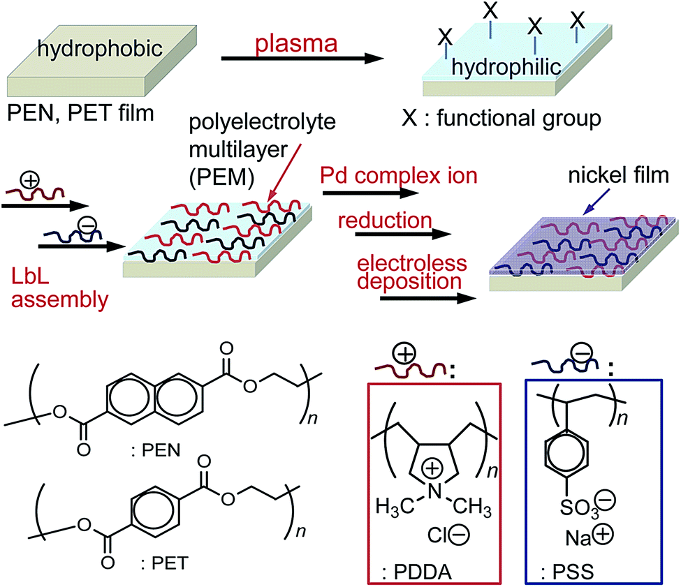 | ||
| Fig. 1 Surface modification of PEN and PET substrates by plasma treatment and LbL assembly of polyelectrolyte multilayer thin films and following electroless nickel deposition. | ||
Experimental
Plasma treatment and UV irradiation
A typical surface modification was performed as follows (Fig. 2-i). PEN films (Teijin DuPont, Teonex Q51 250 μm) and PET films (Toray, Lumirror S10 250 μm) were cleaned by sonication in acetone for 60 s and in deionized (DI) water for 60 s prior to use. PEN and PET films (25 mm × 25 mm) were treated with a Sakigake-Semiconductor desktop vacuum plasma YHS-R (45 W) for 1 min. For UV irradiation, PEN and PET films were treated with a SEN Lights low pressure Hg arc lamp SUV110GS-36L (250 W, 254 and 185 nm) at a lamp-sample distance of 7 mm for 20 min under air. | ||
| Fig. 2 Schematic illustration for LbL assembly of polyelectrolyte multilayer thin films on plasma-treated substrate surfaces and following electroless nickel deposition. | ||
LbL assembly of polyelectrolyte multilayers
The plasma-treated substrates were immersed in a 0.3 wt% solution of poly(diallyldimethylammonium chloride) [PDDA; Aldrich; MW 200![[thin space (1/6-em)]](https://www.rsc.org/images/entities/char_2009.gif) 000–350000; Fig. 1] containing 1 M NaCl in DI water for 5 min, and washed with DI water. The substrates were then immersed in a 0.2 wt% solution of poly(sodium-p-styrenesulfonate) [PSSNa; Scientific Polymer Products Inc.; MW 500000] containing 1 M NaCl in deionized water for 5 min, and washed with DI water. This immersion cycle was repeated several times (Fig. 2-ii).
000–350000; Fig. 1] containing 1 M NaCl in DI water for 5 min, and washed with DI water. The substrates were then immersed in a 0.2 wt% solution of poly(sodium-p-styrenesulfonate) [PSSNa; Scientific Polymer Products Inc.; MW 500000] containing 1 M NaCl in deionized water for 5 min, and washed with DI water. This immersion cycle was repeated several times (Fig. 2-ii).
Surface characterization
Surface composition of the substrates was analyzed by measuring atomic ratios with a KRATOS AXIS Ultra DLD X-ray photoelectron spectrometer. A JEOL field-emission scanning electron microscope (FE-SEM) JSM-6700F was used for the observation of structural morphologies of the substrate surfaces. Contact angles of the substrate surfaces with water droplets were measured with a Kyowa Kaimen CA-X contact angle meter to estimate surface hydrophilicity.Electroless nickel deposition
Two solutions of palladium complex ion were prepared using Pd(NH3)4Cl2 (10 mM) and PdCl2 (10 mM)–HCl (20 mM) in DI water. The PEN and PET substrates modified with the multilayers were immersed in the freshly prepared palladium complex ion solution for 1 h at room temperature and then in a solution of NaH2PO2 (0.27 M) at 60 °C for 3 min (Fig. 2-iii and iv). The substrates were dipped into an electroless nickel bath at 80 °C for 2–5 min (Fig. 2-v). The electroless nickel bath contained NiCl2 (16 g dm−3), disodium succinate (16 g dm−3), malic acid (18 g dm−3), and NaH2PO2 (24 g dm−3). The pH of the electroless nickel bath was adjusted to 5.6 ± 0.1 using NaOH. The adhesion between the nickel film and the PEN and PET substrates was evaluated through a peel adhesion test using 3M tape. In the test, copper film (20 mm × 10 mm) was scored into 1 mm × 1 mm squares, after which tape was applied to the cut surface and then peeled off.Results and discussion
The PEN and PET substrates were treated with vacuum plasma for 1 min. The contact angles of each substrate with a water droplet decreased (<10°, Table 1), indicating that the surfaces became hydrophilic. The surfaces of the substrates were analyzed by X-ray photoelectron spectroscopy (XPS) as shown in Table 1. The C to O atomic ratio decreased after plasma treatment, suggesting the formation of C–O and C![[double bond, length as m-dash]](https://www.rsc.org/images/entities/char_e001.gif) O bonds at the plasma-treated substrate surfaces resulting from oxygenation of PEN and PET as reported in the literature.4,5,7,43 We reported that the FE-SEM image of surfaces of the PEN and PET substrates before and after plasma treatment for 5 min shows the formation of fibrillar patterns (nanofibrils) consists of relatively polar low-molecular-weight fragments resulting from the scission of the polymer chain by plasma treatment.2,6,10,42 These results show that the surfaces of PEN and PET substrates are etched by the oxygen plasma leading to the formation of polymer chains containing hydrophilic groups such as hydroxyls and carboxyls. The substrates were also irradiated with a low-pressure Hg lamp. The UV-irradiated PEN and PET substrate surfaces became hydrophilic, whereas contact angles decreased up to 19° and 33° respectively, even after prolonged irradiation (Table 1). In the UV-irradiation, active oxygen species such as ozone would oxidize the surface of PEN and PET substrates and enhanced surface hydrophilicity, though not to the degree of the plasma treated substrates.10,40
O bonds at the plasma-treated substrate surfaces resulting from oxygenation of PEN and PET as reported in the literature.4,5,7,43 We reported that the FE-SEM image of surfaces of the PEN and PET substrates before and after plasma treatment for 5 min shows the formation of fibrillar patterns (nanofibrils) consists of relatively polar low-molecular-weight fragments resulting from the scission of the polymer chain by plasma treatment.2,6,10,42 These results show that the surfaces of PEN and PET substrates are etched by the oxygen plasma leading to the formation of polymer chains containing hydrophilic groups such as hydroxyls and carboxyls. The substrates were also irradiated with a low-pressure Hg lamp. The UV-irradiated PEN and PET substrate surfaces became hydrophilic, whereas contact angles decreased up to 19° and 33° respectively, even after prolonged irradiation (Table 1). In the UV-irradiation, active oxygen species such as ozone would oxidize the surface of PEN and PET substrates and enhanced surface hydrophilicity, though not to the degree of the plasma treated substrates.10,40
| Substrate (treatment) | Contact anglea (deg) | Fraction of total elementsb (%) | C/O | N/S | ||||||
|---|---|---|---|---|---|---|---|---|---|---|
| C | O | N | S | Cl | Na | Pd | ||||
| a Contact angles against water droplet.b Determined by XPS analysis.c Substrates modified with multilayers were immersed in palladium complex ion solutions and then in NaH2PO2 solution.d Substrates modified with multilayers were immersed in palladium complex ion solutions. | ||||||||||
| PEN (as-received) | 80 | 78.7 | 21.3 | 0 | 0 | 0 | 0 | 0 | 3.7 | |
| PEN (plasma, for 1 min) | <10 | 73.0 | 25.8 | 1.0 | 0 | 0 | 0 | 0 | 2.8 | |
| PEN (UV, for 20 min) | 19 | |||||||||
| PEN (PDDA/PSS)3.5 | 77.5 | 12.0 | 5.9 | 3.2 | 1.4 | 0 | 0 | 1.8 | ||
| PEN (PDDA/PSS)3.5-[PdCl4]2−c |
71.0 | 19 | 5.4 | 2.5 | 0.1 | 0 | 1.6 | |||
| PEN (PDDA/PSS)3.5-[Pd(NH3)4]2+c |
75.6 | 15.8 | 5.6 | 2.8 | 0.1 | 0 | 0 | |||
| PEN (PDDA/PSS)4 | 71.1 | 17.8 | 3.5 | 4.8 | 0 | 2.8 | 0 | 0.73 | ||
| PEN (PDDA/PSS)4-[PdCl4]2−c |
76.3 | 14.6 | 4.5 | 4.2 | 0 | 0.2 | 0.2 | |||
| PEN (PDDA/PSS)4-[Pd(NH3)4]2+c |
74.4 | 15.9 | 3.9 | 4.4 | 0 | 1.3 | 0.1 | |||
| PEN (PDDA/PSS)4-[Pd(NH3)4]2+ (before reduction)d | 73.7 | 15.6 | 5.4 | 4.6 | 0 | 0 | 0.6 | |||
| PET (as-received) | 80 | 72.7 | 27.3 | 0 | 0 | 0 | 0 | 0 | 2.7 | |
| PET (plasma, for 1 min) | <10 | 67.3 | 31.6 | 1.1 | 0 | 0 | 0 | 0 | 2.1 | |
| PET (UV, for 20 min) | 33 | |||||||||
On the surface of the plasma-treated substrates, polyelectrolyte multilayer thin films were acquired via LbL assembly of PDDA and PSS, which are the most commonly used and permanently charged polyelectrolytes (Fig. 1). The multilayers were formed with four layers of polycation PDDA and alternating four or three layers of polyanion PSS (i.e. 4 or 3.5 bilayers of PDDA/PSS). Bilayers containing four layers of both PDDA and PSS, referred to as (PDDA/PSS)4, had a PSS outermost layer, and (PDDA/PSS)3.5, with four layers of PDDA and three of PSS, had a PDDA outermost layer. It is expected that (PDDA/PSS)4 has a negatively charged surface for the PSS outermost layer, and (PDDA/PSS)3.5 has a positively charged surface for the PDDA outermost layer. It was reported that surface charge of multilayers alternates when passing from a multilayer ending with a polyanion to a multilayer ending with a polycation. Decher et al. studied alternating change of the surface charge by ζ potential measurements in detail.33,36 It is reasonable to assume that the charge brought by each polyelectrolyte serves to compensate the excess charge of the multilayers leading to growth of the multilayer accompanied by a new excess charge of opposite sign. Recently, model of charge overcompensation for each layer has been discussed in detail.34,36,38 It was also reported that thickness and morphology of a multilayer depend on ionic strength and electrolyte species.35,39 Multilayers prepared in a high concentration NaCl solution are thicker and have a higher surface roughness. We prepared multilayers (PDDA/PSS)3.5 and (PDDA/PSS)4 from the solution of each polyelectrolyte containing NaCl (1 M) to form thicker layers that ensure complete coverage and eliminate any substrate surface effects and then enhance the reproducibility of the properties of the multilayers.
The PEN and PET substrates modified with the multilayers were activated by forming palladium nanoparticles for electroless nickel deposition. The PEN substrate with the multilayer (PDDA/PSS)3.5 was immersed in a negatively charged palladium complex ion, [PdCl4]2− solution and then in NaH2PO2 solution. Thus, just after immersing the substrate into an electroless deposition bath, a nickel film started to be deposited on the substrate surfaces. After immersing for 2 min, the nickel film (thickness ca. 0.5 μm) was free of cracks and defects as shown in Fig. 3a. A peel adhesion test showed that the nickel film was adhesive to the PEN substrate. In contrast, nickel films were not deposited on (PDDA/PSS)3.5 with a positive palladium complex ion [Pd(NH3)4]2+ (Fig. 3b). On the surface of (PDDA/PSS)4 with a positively charged catalyst [Pd(NH3)4]2+, it took several ten seconds to start the deposition of nickel films and uniform nickel films were formed after immersing for 5 min (Fig. 3d), showing that catalytic activity of the surface of (PDDA/PSS)4 with [Pd(NH3)4]2+ is lower than that of (PDDA/PSS)3.5 with [PdCl4]2−. Some nickel films that contain cracks and defects were deposited on the surface of (PDDA/PSS)4 with [PdCl4]2− (Fig. 3c). Electroless nickel deposition of the PET substrates modified with the multilayers also gave similar results. These results show that multilayer surfaces selectively bind oppositely charged palladium complex ions,24,25 which are reduced by NaH2PO2 to form palladium-nanoparticles and to function as the catalyst for starting nickel deposition (Fig. 2). Binding selectivity of [PdCl4]2− is lower than that of [Pd(NH3)4]2+, possibly due to nonselective binding of [PdCl4]2− to charged polymer surface as reported in previous papers.24,44 Similar results in the PEN and PET substrates show that the binding selectivity of Pd ion complex depends on the properties of the multilayers, but not on those of the substrates.
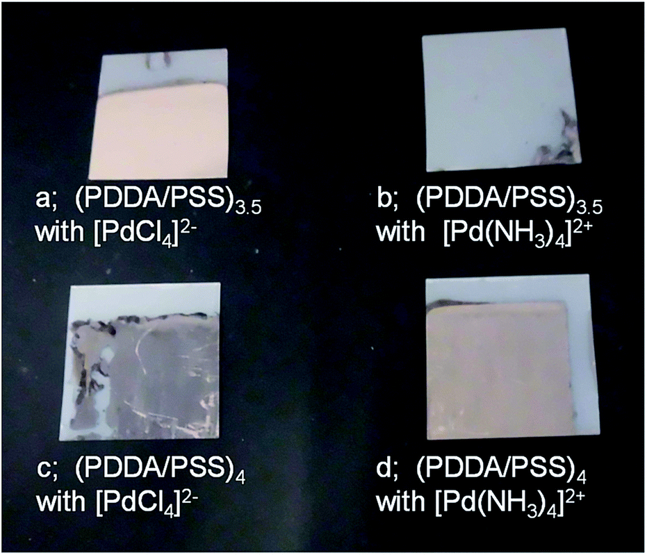 | ||
| Fig. 3 Nickel deposited PEN substrates modified with the multilayers: (a) (PDDA/PSS)3.5 with [PdCl4]2−; (b) (PDDA/PSS)3.5 with [Pd(NH3)4]2+; (c) (PDDA/PSS)4 with [PdCl4]2−; (d) (PDDA/PSS)4 with [Pd(NH3)4]2+. | ||
The structure of the multilayers and the polymer surfaces affected the nickel deposition as shown below. In multilayers assembled without NaCl, nickel films were deposited on the substrate surface, though the reproducibility of the uniformity of deposited nickel films was lower, in contrast to that of the multilayers assembled in the presence of NaCl. The multilayers assembled without NaCl could not cover the substrate surface completely.
Nickel films were deposited also on the multilayers (PDDA/PSS)3.5 with [PdCl4]2− assembled on UV-irradiated PEN and PET substrate surfaces, although the nickel films contained defects and were not adhesive to the substrates. These results are in contrast to those on the multilayers assembled on the plasma-treated PEN and PET substrates. The plasma-treated PEN substrate was immersed in [Pd(NH3)4]2+ solution and then in NaH2PO2 solution. Nickel films were deposited much more slowly and incompletely on the plasma-treated PEN surface than on the PEN surface with multilayers. The plasma-treated PEN surface, which has a negative charge due to carboxylic acid group, is relatively ineffective at binding the [Pd(NH3)4]2+ catalyst. All these results show that the multilayers on plasma-treated PEN and PET surface are suitable for supporting palladium nanoparticle catalysts and their properties are changed by the condition of LbL assembly.
The surfaces of the PEN substrate modified with the multilayers before and after forming palladium nanoparticles were observed by FE-SEM (Fig. 4). Before forming palladium nanoparticles, granular patterns were observed both on (PDDA/PSS)3.5 and on (PDDA/PSS)4 (Fig. 4b and e). The surface of (PDDA/PSS)4 was rougher than that of (PDDA/PSS)3.5. This will be for difference of an outermost layer. It was reported that roughness generated by anisotropic swelling due to water is preserved by PSS layer.39 After binding palladium complex ions and their reduction by NaH2PO2, particles that are considered to be aggregated palladium nanoparticles (diameter of the cluster > ca. 10 nm) were found on (PDDA/PSS)3.5 with [PdCl4]2− and (PDDA/PSS)4 with [Pd(NH3)4]2+ (Fig. 4c and g), but neither on (PDDA/PSS)3.5 with [Pd(NH3)4]2+ nor on (PDDA/PSS)4 with [PdCl4]2− (Fig. 4d and f). This corresponds to the result of the nickel deposition (Fig. 3). That is to say, palladium complex ions bind to oppositely charged multilayer surfaces selectively and are reduced to form palladium nanoparticles.
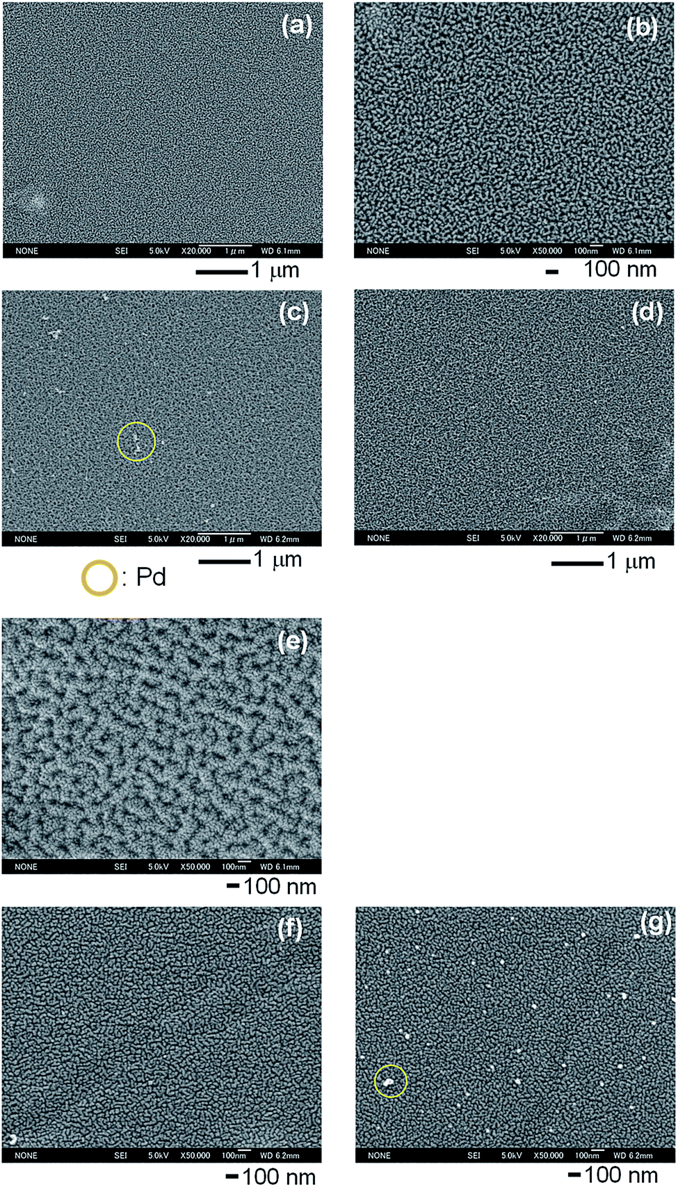 | ||
| Fig. 4 FE-SEM images of the surface of PEN substrates modified with the multilayers: (a) (PDDA/PSS)3.5 (×20k); (b) (PDDA/PSS)3.5 (×50k); (c) (PDDA/PSS)3.5 with [PdCl4]2−; (d) (PDDA/PSS)3.5 with [Pd(NH3)4]2+; (e) (PDDA/PSS)4; (f) (PDDA/PSS)4 with [PdCl4]2−; (g) (PDDA/PSS)4 with [Pd(NH3)4]2+. | ||
The surfaces of the PEN substrate modified with the multilayers were also analyzed by XPS (Table 1). Atomic ratio determined by XPS shows that the growth of the multilayer is accompanied by charge overcompensation during alternating adsorption of PDDA and PSS.38,40 The counterions of the –NR3+ group, Cl− ions, are detected exclusively on the surface of (PDDA/PSS)3.5, while the counterions of the –SO3− groups, Na+ ions, are exclusively detected on the surface of (PDDA/PSS)4. S and N are unique to PSS and PDDA, respectively. The N to S atomic ratio decreases from 1.8 for the (PDDA/PSS)3.5 surface to 0.73 for the (PDDA/PSS)4 surface, thus indicating that the deposition of PSS to the (PDDA/PSS)3.5 surface, which consists of PDDA predominantly and is positively charged, results in charge overcompensation to form the (PDDA/PSS)4 surface, which consists of PSS predominantly and is negatively charged. The surface charge overcompensation forms uncompensated –NR3+Cl− groups on the PDDA-capped surface of (PDDA/PSS)3.5 and uncompensated –SO3−Na+ groups on the PSS-capped surface of (PDDA/PSS)4.
The XPS analysis of the PEN substrate activated by forming palladium nanoparticles shows that Pd exists on the surface of (PDDA/PSS)3.5 with [PdCl4]2−, but not on (PDDA/PSS)3.5 with [Pd(NH3)4]2+ (Table 1). This corresponds to the result of the nickel deposition (Fig. 3) and will be due to the binding selectivity of palladium complex ions. In contrast, little palladium exists on the surface of (PDDA/PSS)4 with [Pd(NH3)4]2+, where nickel film could be electrolessly deposited. It is considered that palladium complex ion or palladium nanoparticles leak off from the (PDDA/PSS)4 during the reduction by NaH2PO2, because Pd exists on (PDDA/PSS)4 with [Pd(NH3)4]2+ before the reduction (Table 1).45,46 The leakage of palladium species could decrease the catalytic activity of the (PDDA/PSS)4 surface as described above. Rough surface of (PDDA/PSS)4 due to a PSS outermost layer might cause the leakage.
From all these results, it is considered that the multilayers and then nickel films are formed on the plasma-treated PEN and PET surfaces as shown below. Hydroxyl (–OH) and carboxyl (–CO2H) groups are uniformly produced on the substrate surfaces as a result of the oxygenation of PEN and PET from plasma treatment and grant hydrophilicity to the substrate surfaces. The initial stage of LbL assembly is adsorption of PDDA to the substrate surface. While adsorbed to the oxygenated surface, an ammonium (–NR3+) group of PDDA interacts with a carboxylate (–CO2−) group to form a (–CO2−)(–NR3+) complex.29 The multilayers are formed by LbL assembly on the oxygenated surface, and the adhesive strength depends on the density of –OH and –CO2H groups because the electrostatic interactions enhance the compatibility between the substrate surfaces and the multilayers. The oxygenated layer and the multilayers, whose thicknesses are estimated to be a several tens nanometer,35 do not affect the bulk properties of the PEN and PET substrates (Fig. 2). In addition, the plasma-etched polymer surface consists of relatively polar low-molecular-weight fragments.3 At the PEN/PDDA interface, electrostatic interaction and entanglements of polymer chains are expected to enhance their compatibility. In contrast, the UV-irradiated PEN and PET surfaces, which have larger contact angles (Table 1), could have a lower density of –OH and –CO2H groups.42 Therefore, nickel films formed on the UV-irradiated surfaces modified with multilayers have defects and are not adhesive to the substrates. Alternatively, the oxygenated-layer formed by UV-irradiation is estimated to have a several hundred nanometer thickness and lower mechanical strength. For the thicker and fragile oxygenated-layer, adhesion strength between metal films and the UV-irradiated substrate surfaces is considered to be low.
The surfaces of multilayers bind oppositely charged palladium complex ions selectively by ion exchange. The surface of (PDDA/PSS)3.5, which consists of PDDA predominantly, is positively charged as described above and binds [PdCl4]2− selectively. On the other hand, negatively charged surface of (PDDA/PSS)4 binds [Pd(NH3)4]2+ selectively. Each palladium complex ion is reduced by NaH2PO2 to form palladium nanoparticles, which function as a catalyst for electroless deposition. In common electroless processes, metals are deposited onto a polymer substrate surface that has a micrometer-scale roughness formed by chemical etching,16 which can affect the physical properties of the metal film and damage the polymer substrate. Our process enables electroless deposition of a nickel film adhesive to a smooth polymer surface without affecting the bulk properties. Possible source for improved adhesion is the decreased stress of nickel films at the multilayer/nickel film interface as compared to that at the bare polymer surface/nickel film interface. The multilayers behave like hydrogels and their plasticization imparts a degree of mobility of the surface conformational accommodation during nickel deposition. Furthermore, the positively charged (PDDA/PSS)3.5 surface is suitable for supporting negatively charged chemical species such as [PdCl4]2−, while the negatively charged (PDDA/PSS)4 surface is suitable for supporting positively charged ones. Therefore, the multilayers, whose properties can be controlled by the condition of LbL assembly, are suitable for supporting a variety of charged chemical species. On the other hand, plasma-treated polymer surfaces are negatively charged due to –CO2H groups in general and suitable only for supporting positively charged chemical species, while a uniform nickel film could not be electrolessly deposited on the plasma-treated PEN substrates with [Pd(NH3)4]2+.
Conclusions
Plasma treatment oxygenated the surfaces of PEN and PET substrates to form hydrophilic surface. The plasma-treated substrate surfaces were compatible with the polyelectrolyte multilayer thin films acquired via LbL assembly. Nickel films were electrolessly deposited on the substrate surfaces modified by multilayers, which are suitable for supporting palladium nanoparticle catalysts. The properties of the multilayers can be controlled by condition of LbL assembly and play an important role in adhesion between the substrates and nickel. This process enables electroless metal deposition on a smooth polymer substrate and could be applicable for manufacturing printed circuits on a flexible film. In addition, this surface modification process is simple, relatively fast, and environmentally benign and should be applicable to the modifications of flexible polymer film surfaces by charged compounds for fabricating devices and biomedical materials.19–23Acknowledgements
This study was partly supported by JSPS KAKENHI Grant Numbers 25410135, 17K05853 and Matching Planner Program from Japan Science and Technology Agency, Grant Number MP27115663514.Notes and references
- J. Friedrich, The Plasma Chemistry of Polymer Surfaces: Advanced Techniques for Surface Design, Wiley, 2012 Search PubMed.
- B. D. Beak, J. S. G. Ling and G. J. Legget, J. Mater. Chem., 1998, 8, 1735 RSC.
- H. M. Powell and J. J. Lannutti, Langmuir, 2003, 19, 9071 CrossRef CAS.
- K. Teshima, H. Sugimura, Y. Inoue, O. Takai and A. Takanao, Langmuir, 2003, 19, 10624 CrossRef CAS.
- E. Gonzalez II, M. D. Barankin, P. C. Guschl and R. F. Hicks, Langmuir, 2008, 24, 12636 CrossRef PubMed.
- E. Wohlfart, J. P. F. Blazquez, E. Knoche, A. Bello, E. Perez, E. Arzt and A. del Campo, Macromolecules, 2010, 43, 9908 CrossRef CAS.
- M. S. Fleischman, B. S. Lee, V. R. Santiago, V. Chhasatia, Y. Sun and D. D. Pappas, Surf. Coat. Technol., 2012, 206, 3923 CrossRef CAS.
- G. H. Yang, E. T. Kang and K. G. Neoh, Langmuir, 2001, 17, 211 CrossRef CAS.
- T. Farhan and W. T. S. Huck, Eur. Polym. J., 2004, 40, 1599 CrossRef CAS.
- H.-Y. Nie, M. J. Walzak, B. Berno and N. S. McIntyre, Appl. Surf. Sci., 1999, 144, 627 CrossRef.
- H. Endo, K. Tashiro, H. Ma, S. Mizuhashi, T. Yamamoto, R. Kimizuka, O. Takai, H. Honma and C. E. Cordonier, J. Electrochem. Soc., 2015, 162, D193 CrossRef CAS.
- H. Sugimura, N. Miki, A. Nakamura and T. Ichii, Chem. Lett., 2014, 43, 1557 CrossRef CAS.
- K. Ohno, Y. Kayama, V. Ladmiral, T. Fukuda and Y. Tsujii, Macromolecules, 2010, 43, 5569 CrossRef CAS.
- M. Kimura, H. Yamagiwa, D. Asakawa, M. Noguchi, T. Kurashina, T. Fukawa and H. Shirai, ACS Appl. Mater. Interfaces, 2010, 2, 3714 CAS.
- N. Ayres, Polym. Chem., 2010, 1, 769 RSC.
- C. A. Deckert, Electroless Copper Plating in ASM Handbook: Surface Engineering, ASM International, 1994, vol. 5, p. 311 Search PubMed.
- S. Siau, A. Vervaet, S. Nalines, E. Schacht and A. Van Calster, J. Electrochem. Soc., 2004, 151, C831 CrossRef CAS.
- G. Decher, J. D. Hong and J. Schmitt, Thin Solid Films, 1992, 210(211), 831 CrossRef.
- I. Lee, Langmuir, 2013, 29, 2476 CrossRef CAS PubMed.
- K. Ariga, Y. Yamauchi, G. Rydzek, Q. Ji, Y. Yonamine, K. C.-W. Wu and J. P. Hill, Chem. Lett., 2014, 43, 36 CrossRef CAS.
- J. Borges and J. F. Mano, Chem. Rev., 2014, 114, 8883 CrossRef CAS PubMed.
- M. Matsusaki, H. Ajiro, T. Kida, T. Serizawa and M. Akashi, Adv. Mater., 2012, 24, 454 CrossRef CAS PubMed.
- P. Bertrand, A. Jonas, A. Laschewsky and R. Legras, Macromol. Rapid Commun., 2000, 21, 319 CrossRef CAS.
- T. C. Wang, B. Chen, M. F. Rubner and R. E. Cohen, Langmuir, 2001, 17, 6610 CrossRef CAS.
- J. S. Ahn, T. R. Hendricks and I. Lee, Adv. Funct. Mater., 2007, 17, 3619 CrossRef CAS.
- K. Cheng, M.-H. Yang, W. W. W. Chiu, C.-Y. Huang, J. Chang, T.-F. Ying and Y. Yang, Macromol. Rapid Commun., 2005, 26, 247 CrossRef CAS.
- T. Tamai, M. Watanabe, S. Watase, N. Nishioka and K. Matsukawa, Electron. Packag., 2011, 4, 110 CAS.
- T. Tamai, M. Watanabe, S. Ikeda, Y. Kobayashi, Y. Fujiwara and K. Matsukawa, Chem. Lett., 2012, 41, 277 CrossRef CAS.
- W. Chen and T. J. McCarthy, Macromolecules, 1997, 30, 78 CrossRef CAS.
- D. A. Hagen, B. Foster, B. Stevens and C. Grunlan, ACS Macro Lett., 2014, 3, 663 CrossRef CAS.
- D. Yoo, S. S. Shiratori and M. F. Rubner, Macromolecules, 1998, 31, 4309 CrossRef CAS.
- S. S. Shiratori and M. F. Rubner, Macromolecules, 2000, 33, 4213 CrossRef CAS.
- G. Ladam, P. Schaad, J. C. Voegel, P. Schaaf, G. Decher and F. Cuisinier, Langmuir, 2000, 16, 1249 CrossRef CAS.
- J. B. Schlenoff and S. T. Dubas, Macromolecules, 2001, 34, 592 CrossRef CAS.
- It was reported that the thickness of (PDDA/PSS)4 from the solution of the polyelectrolytes containing NaCl (1 M) is 40 nm; R. A. McAloney, M. Sinyor, V. Dudnik and M. C. Goh, Langmuir, 2001, 17, 6655 CrossRef CAS . Similar results were also reported in ref. 34, 36 and 41.
- M. Adusumilli and M. L. Bruening, Langmuir, 2009, 25, 7478 CrossRef CAS PubMed.
- X. Zan, D. A. Hoagland, T. Wang and Z. Su, Macromolecules, 2012, 45, 8805 CrossRef CAS.
- R. A. Ghostine, M. Z. Markarian and J. B. Schlenoff, J. Am. Chem. Soc., 2013, 135, 7636 CrossRef CAS PubMed.
- R. A. Ghostine, R. M. Jisr, A. Lehaf and J. B. Schlenoff, Langmuir, 2013, 29, 11742 CrossRef CAS PubMed.
- X. Liu, C. Leng, L. Yu, K. He, L. J. Brown, Z. Chen, J. Cho and D. Wang, Angew. Chem., 2015, 127, 4933 CrossRef.
- A. Ge, M. Matsusaki, L. Qiao, M. Akashi and S. Ye, Langmuir, 2016, 32, 3803 CrossRef CAS PubMed.
- T. Tamai, M. Watanabe and K. Mitamura, Colloid Polym. Sci., 2015, 293, 1349 CAS.
- Residual air in the vacuum plasma apparatus chamber is likely to form oxygen and nitrogen plasma, and then oxygen and nitrogen atoms could be introduced to the polymer surface.
- T. Tamai, M. Watanabe, Y. Hatanaka, H. Tsujiwaki, N. Nishioka and K. Matsukawa, Langmuir, 2008, 24, 14203 CrossRef CAS PubMed.
- When the reduction was omitted and a substrate PEN-(PDDA/PSS)4-[Pd(NH3)4]2+ was immersed into an electroless deposition bath, the deposition bath became unstable and decomposed. Palladium species would leak from the multilayers. This shows that the reduction of palladium complex ions is indispensable for the electroless deposition.
- Alternatively, the change of the (PDDA/PSS)4 surface structure due to polyelectrolyte diffusion might result in decreasing the density of Pd. It was reported that the surface structure of the PSS-capped multilayer prepared in a higher concentration NaCl solution changes after aging for a week.41 The polyelectrolyte chain diffusion in multilayers forms a polyelectrolyte mixture on their surface. Before XPS measurement, our samples were stored in a desiccator for 24 h under atmospheric pressure and in an XPS equipment for 24 h under vacuum.
| This journal is © The Royal Society of Chemistry 2017 |