
 Open Access Article
 This Open Access Article is licensed under a Creative Commons Attribution-Non Commercial 3.0 Unported Licence
Uniform coating of TiO2 on high aspect ratio substrates with complex morphology by vertical forced-flow atomic layer deposition
Kuang-I. Liua,
Chi-Chung Keib,
Mrinalini Mishra a,
Po-Hsun Chena,
Wei-Szu Liua and
Tsong-Pyng Perng*a
a,
Po-Hsun Chena,
Wei-Szu Liua and
Tsong-Pyng Perng*a
aDepartment of Materials Science and Engineering, National Tsing Hua University, Hsinchu 300, Taiwan. E-mail: tpperng@mx.nthu.du.tw; Fax: +886-3-5723857; Tel: +886-3-5742634
bInstrument Technology Research Center, National Applied Research Laboratories, Hsinchu 300, Taiwan
First published on 11th July 2017
Abstract
This study reports a novel forced-flow atomic layer deposition (ALD) process in which the precursors are forced to flow vertically through the highly porous substrate. The uniform coating in the interior of the hollow fiber membrane (length: 10 cm) indicates that the precursors are able to permeate through the pores within the membrane. Besides enabling faster processing, the new reactor design also improves precursor utilization efficiency. The new novel ALD reactor equipped with multiple reactors to increase the throughput offers a more uniform coating with good conformality on macroscopically 3-dimensional complex substrates with high aspect ratio. The improvement gained by this new reactor design brings a new research field for coating on 3-dimensional complex porous substrates.
Introduction
Conformal thin film coatings that closely follows the morphology of the underlying structure is a crucial technology for fabricating nanoscale components. The deposition methods available for the growth of thin films can be basically divided into physical and chemical processes. For the conventional physical vapor deposition (PVD) process, it is a line-of-sight deposition technique that does not permit conformal deposition throughout the matrix.1,2 In the chemical vapor deposition (CVD) process, depletion of precursor frequently limits uniform coating on a large surface area and it consumes precursors rapidly.3,4 Due to the limitations of these traditional deposition techniques, it is difficult to produce films with a smooth outer surface and a uniform thickness on nanostructured substrates.ALD is an attractive technique that can satisfy these requirements because of the nature of its surface-controlled process, such as atomic scale deposition, uniform film thickness, precise control of growth rate, variable composition control over a large range, and good conformality on substrate with complex topology.5–9 Therefore, ALD is an ideal technique to grow conformal coatings of oxides, nitrides, sulfides, etc.10,11 The deposition process involves dosing with a first reactant which is chemisorbed onto the substrate surface to form a (sub)monolayer. After a purge to remove excess reactant, a second reactant is introduced to form the species of interest by reacting with the already chemisorbed layer. The surface-limiting nature of the reaction achieved through alternate pulsing of the precursors results in the growth of films with excellent large-area uniformity and high conformality,12–16 offering a major advantage over line-of-site techniques such as sputtering and molecular beam epitaxy. An additional benefit of ALD is that the deposition can be conducted at relatively low temperatures than other vacuum deposition techniques such as PVD and CVD, which guarantees low interdiffusion and the possibility to use organic or biological substrates.17–19
Based on the flow path of precursor, two mainstream designs of ALD system have been categorized. The perpendicular-flow ALD has a flow path of precursor along the normal of substrate. On the other hand, the flow path of reactant in the cross-flow ALD is directed along the substrate surface. The traditional ALD can provide excellent coating conformality over planar structures on Si wafer for semiconductor applications. For high aspect-ratio substrates with complex morphology, however, only near the top surface region is coated due to low partial pressure of precursors. Therefore, it is not a time- and cost-effective way to obtain conformal coating on 3-dimensional nanostructured substrates with high aspect ratio by conventional ALD.
Ritala et al.20 shortened the pulse time of ALD reaction, in which the precursors are forced to flow through the anodized aluminum oxide membrane from one side to the other. By this design, the precursor molecules transport faster to the pore wall inside the substrate, as compared to the diffusion process in conventional reactors. In this study, we report and demonstrate a new reactor design which enables rapid and uniform ALD coating on high aspect-ratio and mesoporous fiber substrates based on the forced-flow concept. A new generation forced-flow ALD system that offers better uniformity and conformality and larger batch production capability is disclosed.
Experimental
A new vertical forced-flow ALD system has been designed, as shown in Fig. 1, in which the precursors are forced to flow through the sample to be coated instead of by the diffusion process in conventional ALD equipment. Fig. 1 shows the gas inlets of non-metal and metal precursors from the right side. The precursors and purge gas then pass through six tubular reactors that can be further expanded to 18 reactors, as shown by the bottom plate. The bottom side is for evacuation. The specimens are placed in different reactors of the chamber to test the uniformity of deposition. TiO2 thin film was coated on Si wafer by ALD using titanium tetrachloride (TiCl4) and H2O as the precursors for Ti and O, respectively, with the substrate temperature set at 100 °C. Each cycle consisted of a TiCl4 precursor pulse of 0.5 s, a purge with N2 for 7 s, followed by a H2O pulse for 0.5 s, and a second purge with N2 for 7 s to remove excess precursor and by-products. For the ALD of TiO2 on polysulfone hollow fibers, it was carried out with the durations of pulse time: 3.5 s and 0.5 s for TiCl4 and H2O, respectively. The temperature of the polymer template was maintained at 100 °C. The base pressure of the chamber was 9 × 10⁻³ torr, and the working pressures of TiCl4 and H2O were controlled at approximately 1 torr and 23 torr, respectively. The TiO2/polysulfone hybrid structure was annealed in N2 at 400 °C without any dwelling time. The structure and composition of the composite sample were analyzed by X-ray diffraction (XRD, Shimadzu XRD 6000) using Cu Kα radiation at 30 kV and 20 mA. The surface morphologies and cross sections of the specimens were examined by field-emission scanning electron microscopy (FESEM, JSE-6500F). The thickness of the films on Si wafer was measured by using an ellipsometer. Transmission electron microscopy (TEM) was conducted on a JEOL-3000F microscope operated at 300 kV.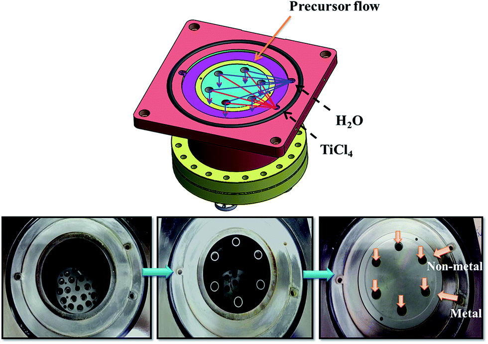 | ||
| Fig. 1 The forced-flow ALD system. The precursors and purge gas pass through six tubular reactors. | ||
Results and discussion
A. TiO2 on Si wafer
In the first example, TiO2 was deposited on silicon wafer. The specimens were vertically placed in different reactors in the chamber to test the uniformity of deposition. Each Si substrate was cut to a dimension of 0.5 cm × 8 cm. To force the precursors flowing through the substrate, the substrates were placed into each of the 6 tube reactors. During the deposition process, the precursors were introduced from the upper part of the chamber, while the downstream of the precursor was continuously pumped away, thereby drawing the precursor and carrier gas molecules to flow through the substrate. Fig. 2 shows that a uniform TiO2 thin film is deposited on Si wafer after 800 cycles of ALD. The surface of TiO2 thin film is very smooth. The TiO2 film thicknesses at various distances from the top end were measured using an ellipsometer (Fig. 3). Within the accuracy of this measurement, the TiO2 film is uniformly coated through the whole substrate. The average thickness of 66.0 nm obtained by 800 cycles corresponds to a growth rate of 0.82 Å per cycle.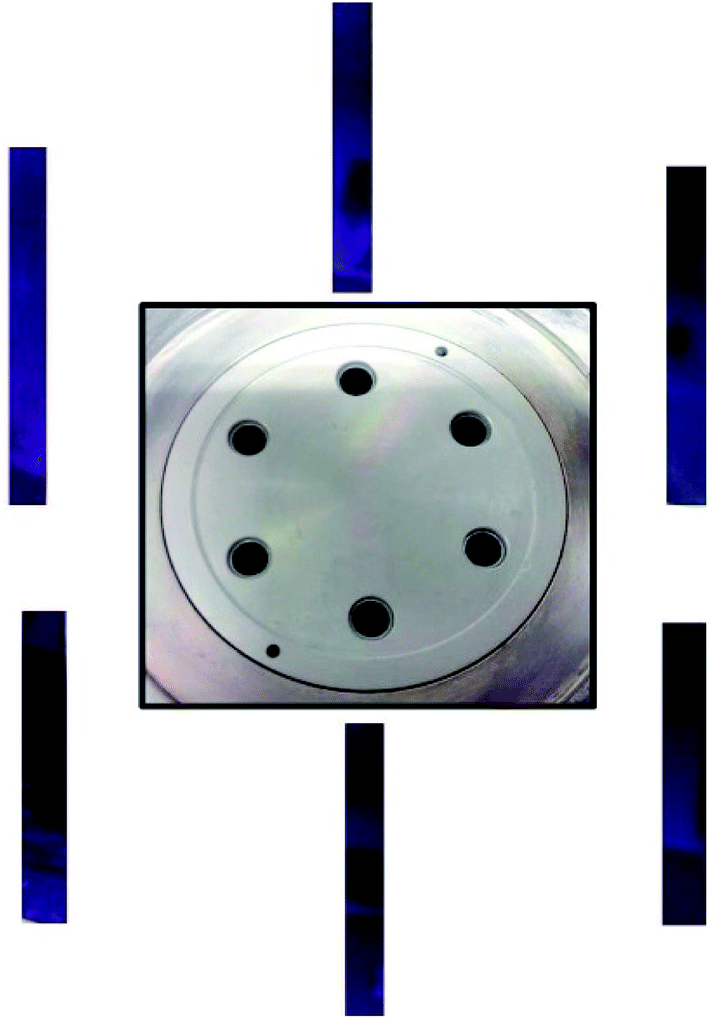 | ||
| Fig. 2 The uniformity test of TiO2 deposited on Si wafer at different locations of the forced-flow ALD chamber. | ||
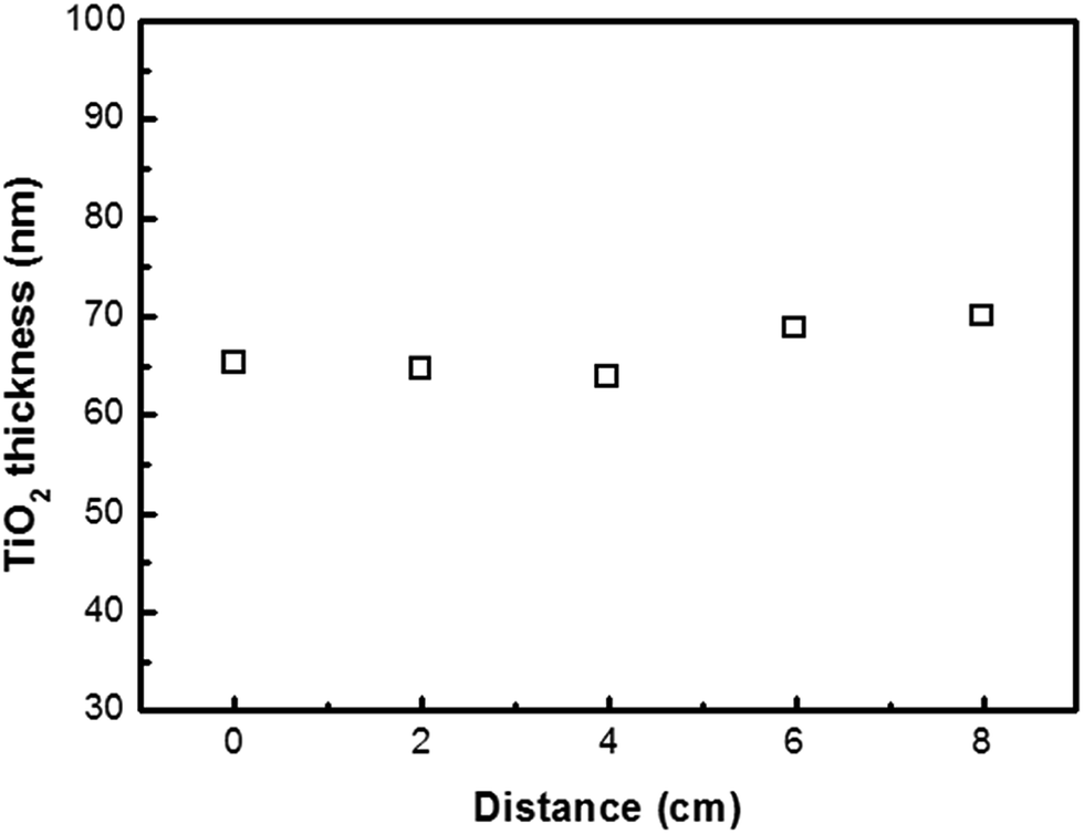 | ||
| Fig. 3 Variation of TiO2 film thickness from the top end of the Si substrate. | ||
B. TiO2 on polysulfone fiber
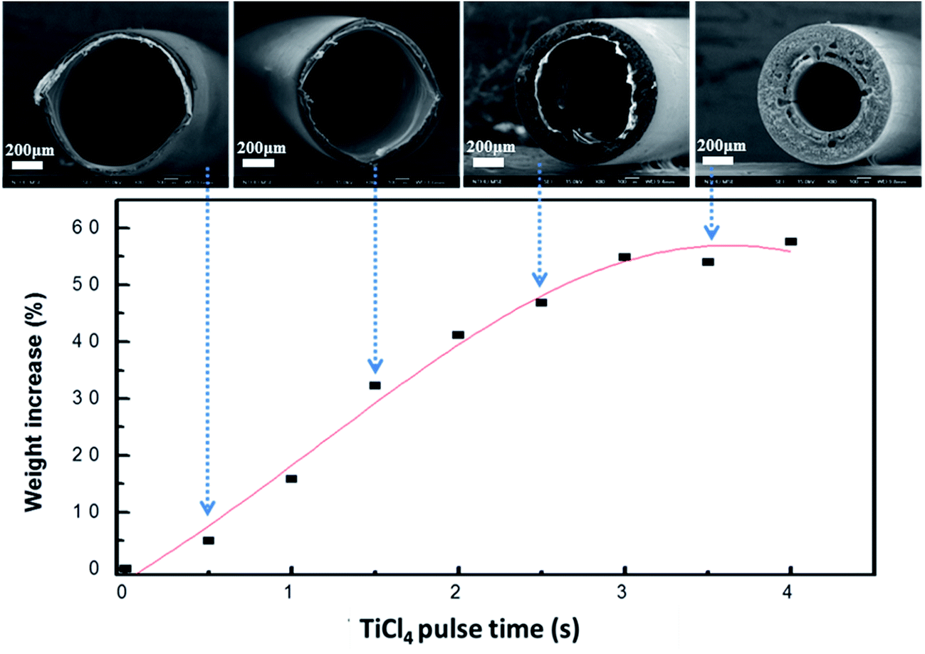
The vertical forced-flow ALD system also offers good uniformity and conformality for hollow fiber substrate with a very high aspect ratio. The SEM images of an individual polysulfone hollow fiber are shown in Fig. 4. The wall is composed of numerous interconnected nanofibers. Fig. 5 presents the ALD saturation curve of TiO2 on the polysulfone hollow fiber membrane template. The weight gain of TiO2 with 400 cycles of deposition saturates at about 3.5 s, showing that further increase in pulse time of the TiCl4 precursor does not thicken the TiO2 coating, which indicates a complete coverage of the precursor molecules on the substrate. The SEM images of the cross sections of the TiO2/polysulfone with various durations of TiCl4 pulse time are also shown in Fig. 5. They are morphologically the same as the polysulfone template, and saturation of TiO2 deposition is reached as the pulse time is increased to 3.5 s. Before reaching the saturated growth rate, the thickness of TiO2 coating was not sufficiently high to maintain the integrity of polysulfone substrate.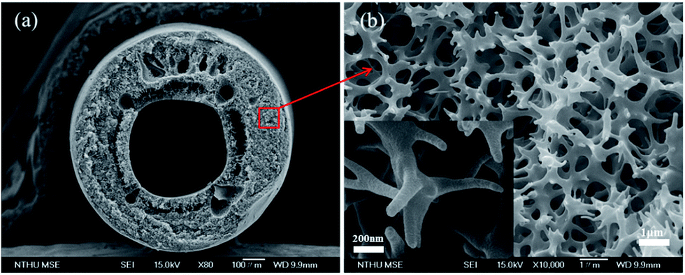 | ||
| Fig. 4 SEM images of a polysulfone fiber. (a) Cross-section and (b) near the middle wall (the inset shows a higher magnification image). | ||
 | ||
| Fig. 5 The ALD saturation curve of TiO2 on polysulfone hollow fiber. The TiCl4 pulse time was varied for depositing 400 cycles of TiO2, while the water pulse time was kept constant. The SEM images show the cross sections of the TiO2/polysulfone hollow fiber with various durations of TiCl4 pulse time. | ||
Fig. 6 shows that a uniform TiO2 thin film is deposited by 400 cycles of forced-flow ALD on a single polysulfone fiber (length: 10 cm) which is used as a template and support. The TiO2/polysulfone hybrid structure was annealed in N2 at 400 °C without any dwelling time. As can be seen, the polymer template is well encapsulated by the TiO2 thin layer along the length. Although the three positions vary remarkably in the distance from the top to the bottom, there is no obvious difference in the morphology and diameter located at different positions. The uniform coating in the interior of the hollow fiber membrane indicates that the precursors are able to permeate through the pores within the membrane and react uniformly with the template surface. It is noted that the polysulfone is preserved to support TiO2 with interconnected internal porous microchannels so that the mechanical properties of TiO2/polysulfone can be improved. Therefore, we have successfully conducted TiO2 coating with a precise control of thickness on a single mesoporous polysulfone hollow fiber based on the forced-flow design. Compared with conventional ALD methods, the present forced-flow ALD system offers the advantages of atomic layer control of film thickness and excellent uniformity and conformality for metal oxide coating on mesoporous substrates with high aspect ratio.
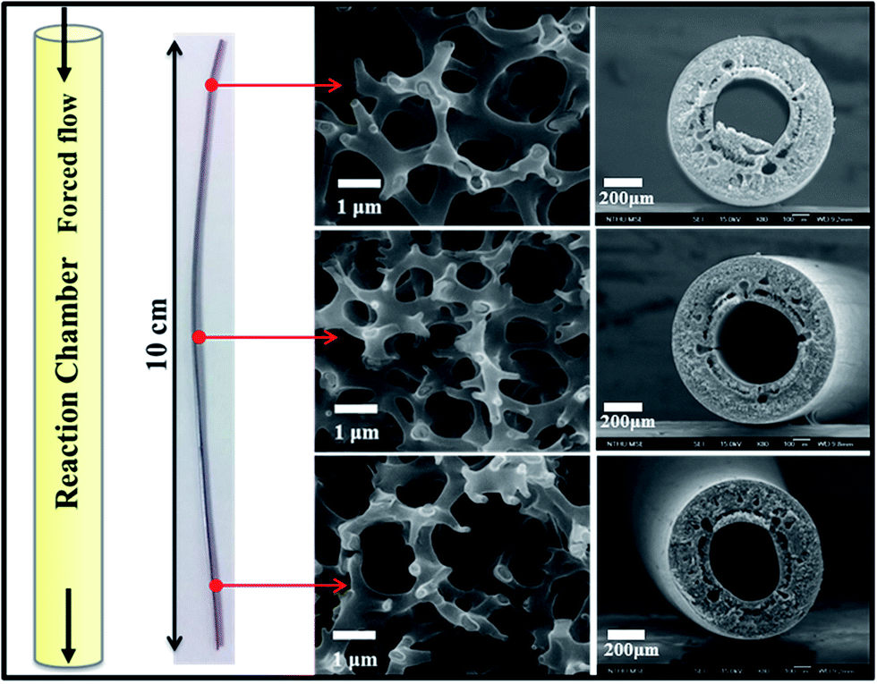 | ||
| Fig. 6 Photo and SEM images of a selected piece of mesoporous TiO2/polysulfone hollow fiber (length: 10 cm) taken at different locations fabricated by the forced-flow ALD system. | ||
As mentioned above, the forced-flow ALD system is equipped with six tubular reactors in the reaction chamber. The next step was to extend to all reactors, and each of them was filled with a bundle of hollow fibers for simultaneous deposition to test the scale-up feasibility. As shown in Fig. 7, a good uniformity was achieved when six tubular reactors were used simultaneously. Indeed, this forced-flow ALD system enables uniform precursor flow along the multi-tube reactors with a high throughput in production that would benefit the ALD system to be applied in the industrial scale.
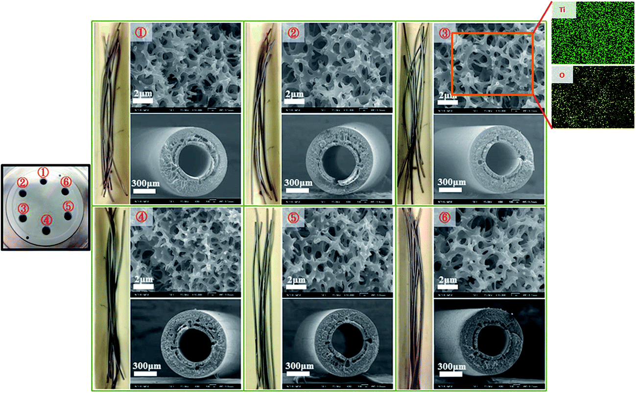 | ||
| Fig. 7 Uniformity test of TiO2 deposited on a bundle of polysulfone hollow fibers in six tubular reactors of the forced-flow ALD chamber. The elemental mappings of Ti and O are shown on the upper right corner. | ||
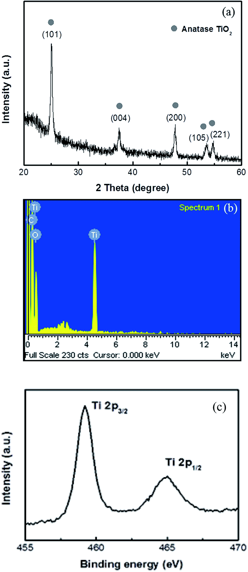
The as-deposited TiO2 by ALD was amorphous. Fig. 8(a) shows the XRD pattern of the TiO2/polysulfone hybrid heated in N2 to 400 °C without any dwelling time. It exhibits a pure anatase phase of TiO2. The chemical composition of the TiO2/polysulfone hybrid was determined using energy dispersive X-ray (EDX) spectrometry, as shown in Fig. 8(b). The peaks of Ti and O can be clearly seen, indicating that the sample contains Ti and O elements. The presence of C can be ascribed to the remaining polysulfone membrane. The X-ray photoelectron spectrum (XPS) of the Ti binding energy shown in Fig. 8(c) further confirms that it is indeed a pure TiO2 phase.
 | ||
| Fig. 8 (a) XRD pattern, (b) EDX spectrum, and (c) XPS of Ti binding energy of TiO2/polysulfone hollow fibers. | ||
The features of the TiO2 hollow fiber with interconnected core–shell nanofibers or interconnected nanotubes can be appreciated by the comparison of the micrographs from SEM and TEM. As mentioned above, a bundle of long-fiber samples can be loaded to each tubular reactor, as shown schematically in Fig. 9(a). Fig. 9(b) shows the SEM image of the cross section of an individual as-prepared TiO2/polysulfone hollow fiber prepared by 400 ALD cycles. It is morphologically the same as that of the polysulfone template, indicating great conformality of the ALD process. Fig. 9(c) shows that the TiO2/polysulfone hollow fiber wall has a porous structure formed by interconnected core–shell nanofibers. The wall thickness of TiO2 coating is estimated to be 22.8 nm, corresponding to 400 ALD cycles of TiO2. The growth rate of TiO2 is estimated to be 0.57 Å per cycle according to the SEM observation, indicating that the polysulfone hollow fiber is a suitable template for the forced-flow ALD process. After annealing at 450 °C for 1 h, the polysulfone template was removed, leaving only TiO2 hollow fiber. A portion of the sample was then examined by TEM, as shown in Fig. 9(d). The wall thickness of a single nanotube is measured to be 22.5 nm, which is consistent with that estimated from the SEM micrograph (Fig. 9(c)). The surface area and average pore size of the bare polysulfone fibers, measured by the BET (Brunauer–Emmett–Teller) analysis, were found to be 11.88 m2 g−1 and 30.0 nm, and those of TiO2-coated fibers were 8.76 m2 g−1 and 24.6 nm, respectively. The reduction of these two values is presumably due to the shrinkage after heating in N2 at 400 °C.
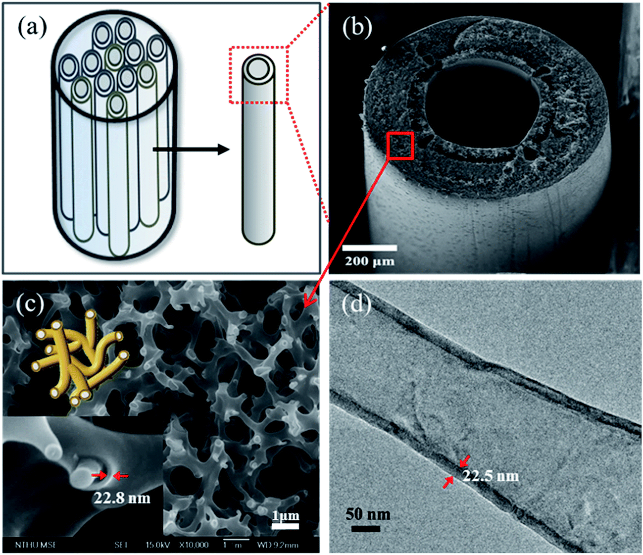 | ||
| Fig. 9 (a) One tubular reactor containing many hollow fibers. (b) SEM image of the cross section of an as-deposited TiO2/polysulfone hollow fiber. (c) Higher magnification image of the TiO2/polysulfone fiber wall. The upper left inset shows that the schematic hollow fiber contains three- dimensional interconnected fibers, and the lower left inset shows the thickness of the TiO2 layer. (d) TEM image of a single nanotube (400 cycles of ALD). | ||
As forced-flow ALD is able to form a conformal coating with precise control over the film thickness at atomic scale on either 2-dimensional or 3-dimensional substrates with a high aspect ratio, it can be extended to prepare many kinds of protection layer, multi-walled nanotubes, and other complex structures for industrial applications.
Conclusion
A new vertical forced-flow ALD system is disclosed, where the precursors are forced to flow through the substrate instead of by diffusion process. Therefore, the deep region of porous nanostructures can be reached by the precursors. This new design offers a higher throughput in production, better uniformity, and good conformality of coating on macroscopically 3-dimensional complex substrates with high aspect ratio, and also improves precursor utilization efficiency. This forced-flow reactor design opens new application areas and is expected to facilitate the development of new nanotechnologies.Acknowledgements
The authors are grateful to Ministry of Science and Technology of Taiwan for supporting this research under the Contract Nos. NSC 99-2221-E-007-066-MY3 and MOST 103-2120-M-007-005.References
- T. S. Cale and G. B. Raupp, J. Vac. Sci. Technol., B: Microelectron. Process. Phenom., 1990, 8, 1242 Search PubMed.
- D. V. Rigney, R. Viguie, D. J. Wortman and D. W. Skelly, J. Therm. Spray Technol., 1997, 6, 167 CrossRef CAS.
- I. A. Shareef, G. W. Rubloff, M. Anderle, W. N. Gill, J. Cotte and D. H. Kim, J. Vac. Sci. Technol., B: Microelectron. Nanometer Struct.--Process., Meas., Phenom., 1995, 13, 1888 CrossRef CAS.
- D. Barreca, L. E. Depero, E. Franzato, G. A. Rizzi, L. Sangaletti, E. Tondello and U. Vettoria, J. Electrochem. Soc., 1999, 146, 551 CrossRef CAS.
- M. Leskelä and M. Ritala, Angew. Chem., Int. Ed., 2003, 42, 5548 CrossRef PubMed.
- H. Kim, J. Vac. Sci. Technol., B: Microelectron. Nanometer Struct.--Process., Meas., Phenom., 2003, 21, 2231 CrossRef CAS.
- M. D. Groner, J. W. Elam, F. H. Fabreguette and S. M. George, Thin Solid Films, 2002, 413, 186 CrossRef CAS.
- D. M. Hausmann and R. G. Gordon, J. Cryst. Growth, 2003, 249, 251–261 CrossRef CAS.
- D. Vogler and P. Doe, Solid State Technol., 2003, 46, 35 Search PubMed.
- R. L. Puurunen, J. Appl. Phys., 2005, 97, 121301 CrossRef.
- M. Ritala and M. Leskelä, Nanotechnology, 1999, 10, 19 CrossRef CAS.
- T. Suntola, Mater. Sci. Rep., 1989, 4, 261 CrossRef CAS.
- S. M. George, A. W. Ott and J. W. Klaus, J. Phys. Chem., 1996, 100, 13121 CrossRef CAS.
- C. Goodman and M. Pessa, J. Appl. Phys., 1986, 60, 65 CrossRef.
- G. N. Parsons, S. M. George and M. Knez, MRS Bull., 2011, 36, 865 CrossRef CAS.
- M. Ritala, K. Kukli, A. Rahtu, P. I. Raisanen, M. Leskela, T. Sajavaara and J. Keinonen, Science, 2000, 288, 319 CrossRef CAS PubMed.
- J. S. Choi, B. S. Yang, S. J. Won, J. R. Kim, S. Suh, H. K. Park, J. Heo and H. J. Kima, ECS Solid State Lett., 2013, 2, 114 CrossRef.
- M. D. Groner, F. H. Fabreguette, J. W. Elam and S. M. George, Chem. Mater., 2004, 16, 639 CrossRef CAS.
- M. Coll, J. Gazquez, A. Palau, M. Varela, X. Obradors and T. Puig, Chem. Mater., 2012, 24, 3732 CrossRef CAS.
- M. Ritala, M. Kemell, M. Lautala, A. Nishanen, M. Leskelä and S. Lindfors, Chem. Vap. Deposition, 2006, 12, 655 CrossRef CAS.
| This journal is © The Royal Society of Chemistry 2017 |