
 Open Access Article
 This Open Access Article is licensed under a
 Creative Commons Attribution 3.0 Unported Licence
A study of the 160 MeV Ni7+swift heavy ion irradiation effect of defect creation and shifting of the phonon modes on MnxZn1–xO thin films†
H. A. Khawal and
B. N. Dole *
*
Advanced Materials Research Laboratory, Department of Physics, Dr Babasaheb Ambedkar Marathwada University, Aurangabad-431 004, India. E-mail: drbndole.phy@gmail.com
First published on 11th July 2017
Abstract
MnxZn1–xO thin films were successfully synthesized by the dip coating technique. The thin films were irradiated by Ni7+ swift heavy ions (SHI) with 1 × 10¹³ ions per cm2 fluence, and their structural, electrical, Raman spectral and surface morphological properties were investigated. X-ray diffraction patterns confirmed the P63mc space groups, and the crystallite size increased after SHI irradiation, due to electron rearrangements. I–V studies revealed enhanced conductivity after Ni7+ SHI irradiation and showed the ohmic nature of the sample. The irradiation sensor efficiency and responsibility were calculated by using I–V data, which revealed impressive results. Photoluminescence (PL) measurements were performed to determine the evolution of defects and defect-annealing during ion irradiation; enhancement in the luminosity of pure and 5% Mn substituted ZnO thin films was observed. The presence of the Raman active strongest optical phonon mode of ZnO at 436.19 cm−1 revealed that ZnO with hexagonal wurtzite structure supported the XRD results. Atomic force microscopy (AFM) images revealed the formation of nano-bunches on the surface and enhanced the surface roughness and skewness of the irradiated samples, due to coulombic interactions between electrons and ions.
Introduction
Nanotechnology is an interdisciplinary research field with vast applications in materials technology, manufacturing, instrumentation, energy production and storage, information technology, chemical technology and the medical field.1–3 However, there are many issues to be addressed, including toxicity and the environmental impact of nanostructured materials and their potential effects on global economics. The many applications of ZnO nanomaterials in spintronic devices, such as optical isolators, spin-valve transistors, non-volatile memory, ultra-fast optical switches and spin-light emitting diodes, inspire extensive research work to synthesize diluted magnetic semiconductors (DMS) with III-V and II-VI semiconductors.4–12 Among the different types of semiconducting nanomaterials, zinc oxide (ZnO) is one of the significant multifunctional materials that finds applications in the various fields. ZnO is cheap in cost and is environmentally friendly as compared to other materials.13 Normally, ZnO is studied on the nanoscale; this is probably because the high surface area to volume ratio of nanoparticles could increase the adsorption of organic pollutants on the surface of the particles, as compared to bulk materials.14–23 ZnO belongs to the group II-VI binary compound semiconductors; in the hexagonal structure it is an n-type semiconductor with high electron mobility, a direct energy bandgap of 3.37 eV and a high exciton binding energy of 60 meV, which is greater than the thermal energy at room temperature. Due to the excellent structural, electrical, optical and morphological properties, ZnO thin films have wide applications as solar cells24 gas sensors,25,26 light emitting diodes (LED's)27 and transparent electrodes.28 Moreover, they can be prepared by different techniques, such as pulsed laser deposition,29 the dip coating method,30 chemical vapor deposition,31 magnetron sputtering,32 the spin coating method,32 atomic layer deposition,33 and thermal evaporation.34 Among the above methods to prepare ZnO, the dip coating method is extremely attractive, due to its features such as its simplicity, low temperature, low cost, easy coating of large surfaces and low evaporation temperature.It is well known that doping a selective element into ZnO has become an important route to improving the structural, electrical, morphological, optical, and magnetic properties, and increasing the carrier concentration for electronic applications because a higher carrier concentration is required. Recently, many studies have been focused on the transition metals (TM) such as Mn, Ni, Fe, Co and Cr doped into ZnO, due to their potential applications in spintronics.35
Swift heavy ions (SHI) are particle radiations accelerated to very high energies, typically in the MeV or GeV range, having sufficient mass and energy to penetrate solid materials. Irradiation with GeV energy ions has been found to produce intermixing in the Fe/Si multilayer (Bauer et al. 1993).36 It was shown by Dunlop et al. (1994)37 that trails of damage can be made in metals by high levels of electronic energy loss, Se. Threshold Se for such columnar damage varies from metal to metal, for example, Se for Fe is ∼5 keV Å−1 (Dunlop et al. 1994). Recently, researchers have shown interest in atomic mixing, materials modification and phase changes using ion beam mixing of high energy, where inelastic collisions or electronic stopping are responsible for the energy loss. Veenu Sisodia and Jain (2004)38 studied mixing induced by swift heavy ion irradiation at Fe/Si interfaces. To date, tubular Mn-doped ZnO structures grown by the solution method have seldom been reported.
In this paper, we propose a new and facile chemical solution method to synthesize the hexagonal Mn-doped ZnO thin films on a large scale, via a dip coating technique. The effect of SHI irradiation on the structural, electrical, morphological and photoluminescence properties of Mn doped ZnO thin films are presented.
Experimental procedure
Synthesis of thin films
Thin films of pure and Mn substituted ZnO, using glass substrates, were synthesized by the dip coating technique that was fully based on the adsorption and reaction of the ions from the solutions. The fundamental building block of the dip coating technique is the collection of samples on the surface of another substance.The pure ZnO thin film was obtained from 0.1 M zinc chloride solution, dissolved in 40 mL distilled water with constant stirring for 1 h at room temperature. Sodium hydroxide (NaOH, 0.1 M) solution was dissolved in 40 mL distilled water for 1 h at 70 °C in a separate beaker. A zincket bath was prepared by adding 2–3 drops of triethanolamine (TEA) and 5–6 drops of ammonia in zinc chloride solution for maintaining the pH at 11. The sodium hydroxide solution was added to the zincket bath and stirred at 80 °C for 1 h using magnetic stirrer. A glass substrate was immersed in hydrochloric acid for 24 h and was subsequently cleaned ultrasonically with acetone and distilled water, and dried on a hot plate at 75 °C for 1 h. The cleaned substrate was dipped in the solution for 30 minutes (three cycles, 10 minute gap) at 80 °C. The film deposited was then dried in air for 60 minutes at 250 °C.
Similarly, for the synthesis of Mn doped ZnO thin films, three solutions, 0.1 M of zinc chloride, 0.1 M of manganese chloride (MnCl2) and NaOH, were separately dissolved in 40 mL of distilled water. NaOH solution was stirred at 70 °C for 1 h; 0.1 M of zinc chloride solution, and 0.1 M of manganese chloride (MnCl2) solution were stirred at room temperature for 1 h, using a magnetic stirrer, then 5% of manganese MnCl2 solution was added into the zinc chloride solution with constant stirring at room temperature. TEA (2 drops) and 5–6 drops of ammonia were added to the zinc chloride solution for preparation of the zincket bath. NaOH solution was added to the zincket bath and stirred at 80 °C for 1 h. The cleaned substrate was dipped in the solution for 30 minutes (10 minute gap, three cycles) at 80 °C. The film was deposited then dried in air for 60 minutes at 250 °C. The manganese concentration was varied up to 5% for the preparation of Mn doped ZnO thin films.
Irradiation experiment
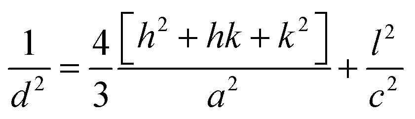
The thin film samples were mounted on an electrically insulated sample ladder and the ladder current was integrated to collect and count the charge pulses via a scalar counter, along with the digital current integrator. The pure and Mn doped ZnO films were irradiated with 160 MeV Ni7+ ions, at room temperature, with fluence of 1 × 10¹³ ions per cm2, using a 15 UD Pelletron accelerator at the Inter-University Accelerator Centre (IUAC), New Delhi, India. The beam current was maintained at 1 pnA (particle nanoampere). This was kept low in order to prevent the sample from heating up during irradiation. The beam was raster scanned over an area of 1 × 1 cm2, using a magnetic scanner. The damage caused by the interaction between the ion beam and target material was calculated using the SRIM software. The electronic stopping power (Se) and nuclear stopping power (Sn) of the 160 MeV Ni7+ ions for pure and Mn doped ZnO films were calculated using SRIM-2008. The range of the projectile ions of Ni7+ for 160 MeV electronic energy loss was 1.033 × 10³ keV μm−1 and nuclear energy loss was 1.42 keV μm−1 and the range was 20.88 μm; ion collision was calculated by depth versus Y axis plot, shown in Fig. 1(a). It was found that the energy loss to target phonons consisted of the direct creation of phonons by the ion and the additional energy loss by target recoil atoms to phonons, as shown in Fig. 1(b).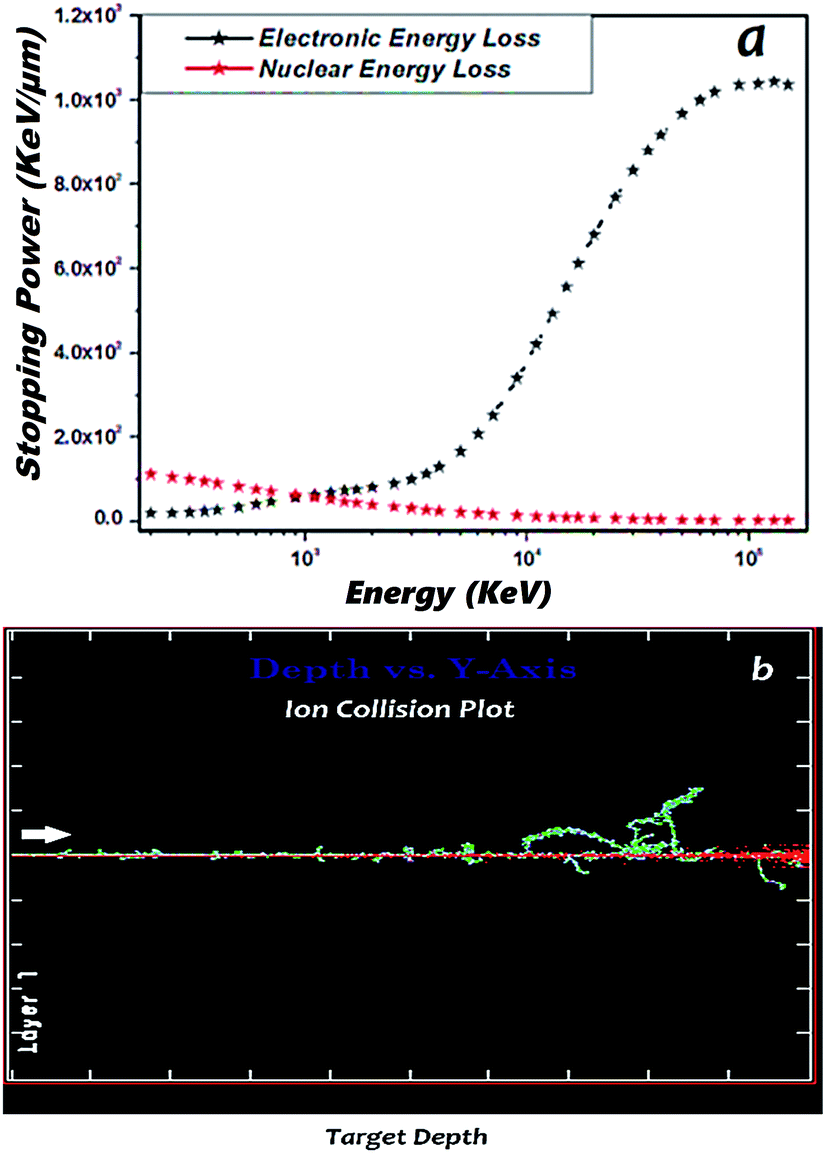 | ||
| Fig. 1 (a) Simulated electronic and nuclear energy loss in the 160 MeV Ni7+ SHI irradiation of ZnO. (b) Ion collision effect of SHI irradiation. | ||
Detailed information for the Li3+ SHI irradiation effect on pure and Mn doped ZnO samples of ion collision, ion recoil distribution, the energy loss of target phonon and energy loss of vacancy production plots can be found in (ESI†).
Material characterization
The pristine and irradiated films were characterized using different techniques. The structural properties were investigated by XRD studies, and patterns were recorded using a D-8 Advance X-ray diffractometer (acquired from Bruker AXS Germany) with the monochromatic CuKα conventional X-ray source, Göbble mirror, LiF monochromator, scintillator detector. I–V measurements were taken at IUAC, New Delhi. Raman spectra of pure and Mn doped ZnO samples were recorded by using an Ar ion laser with 514.5 nm wavelength and 50 mW power as the excitation source. Surface morphologies were studied by atomic force microscopy (AFM) in the tapping mode with an antimony-doped silicon tip, using a Nanoscope.Results and discussion
Crystallographic analysis
X-ray diffraction patterns were used to investigate the crystallographic structure of the as-synthesized samples. The X-ray diffraction patterns were obtained for pristine and Zn1–xMnxO with nominal composition (x = 0.05) irradiated with SHI Ni7+ ions. The X-ray diffraction patterns of the pristine and irradiated, pure and 5% Mn doped ZnO thin films are shown in Fig. 3. The patterns show strong and sharp diffraction peaks, demonstrating good crystallinity, and are matched with the common ZnO hexagonal phase, i.e., the wurtzite structure [80-0074, JCPDS]. These peaks, at angles (2θ) of 31.890, 34.430 36.330, 47.630, 56.730 and 62.960, correspond to the diffractions from the (100), (002), (101), (102), (110) and (103) planes. Pure and 5% Mn doped ZnO samples usually have decreased intensity after SHI irradiation, as reported by S. K. Neogi et al.,39 but in our case, it was observed that the increase in intensity accounted for the influence of ions on the scattering factors of the unit cell. Enhancement in the intensity may also be due to changes in the electronic density in the crystallographic position and the increase in peak intensity is an indication of the improvement of the crystallinity of the samples. The absence of the diffraction peaks of manganese oxide (Mn) structures in the XRD pattern may imply Mn incorporation within the ZnO thin films by means of substitution for Zn, or that the content of the manganese impurities is lower than the limitation of the XRD. The lattice parameters for hexagonal Mn doped ZnO thin films were calculated from the (102) plane. Lattice parameters (a and c) were calculated from XRD data using eqn (1).40
 | (1) |
 | ||
| Fig. 2 Creation of voids in Mn doped ZnO samples after SHI irradiation. | ||
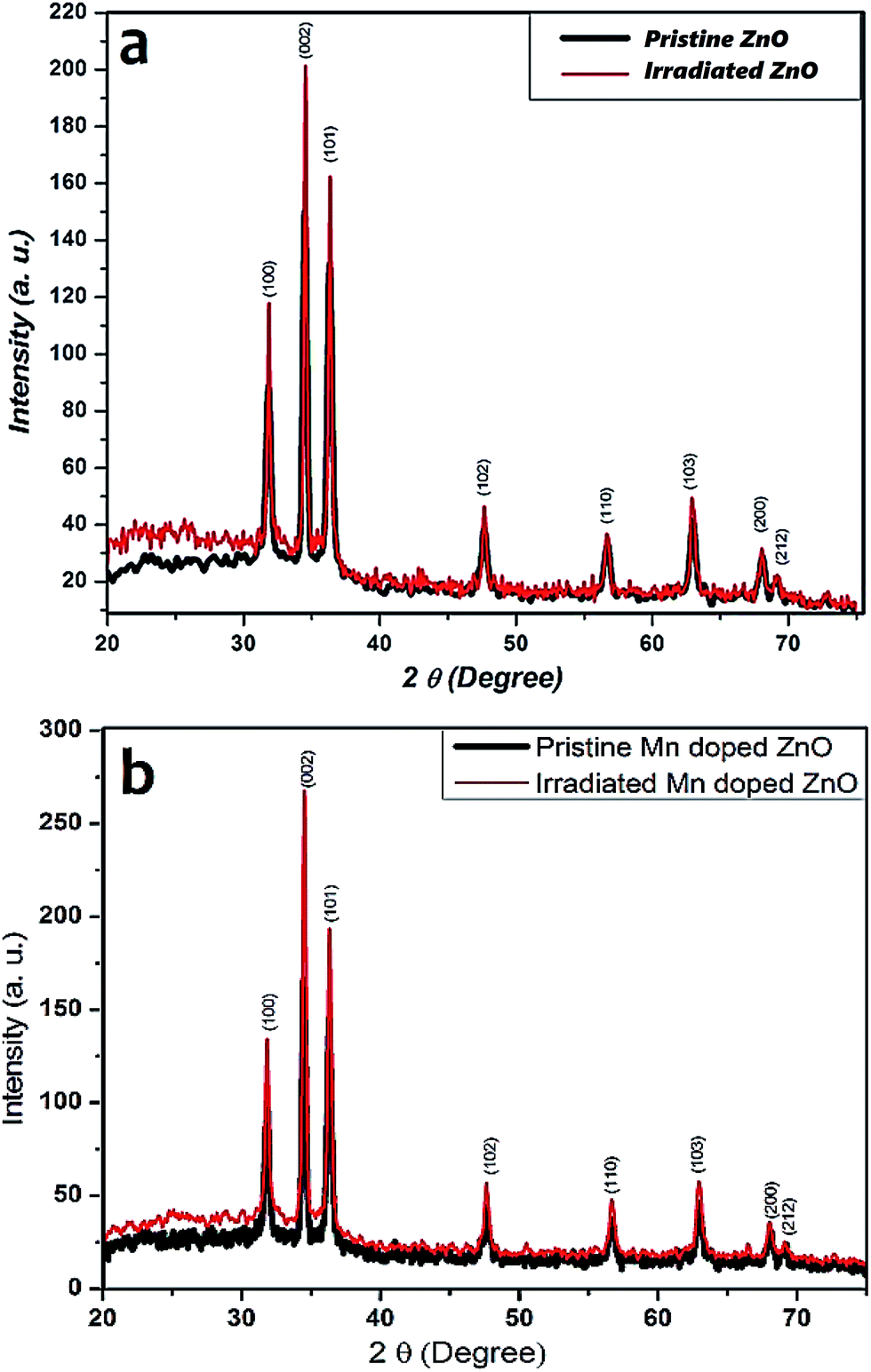 | ||
| Fig. 3 XRD patterns of (a) pristine and irradiated ZnO, (b) pristine and irradiated 5% Mn doped ZnO thin films. | ||
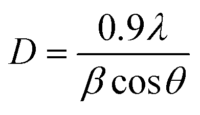
The crystallite sizes of pure and Mn doped ZnO, pristine and irradiated thin films were calculated using the Debye–Scherrer formula:42
 | (2) |
The dislocation density was calculated as the amount of defects in the crystal, or the irregularity within a crystal structure. Dislocations are a type of topological defect. The movement of a dislocation is impeded by other dislocations present in the sample; thus, a larger dislocation density implies a greater hardness. The dislocation density represents the magnitude of defects in the film. The dislocation density was calculated by using the following formula:44
 | (3) |
The X-ray density ‘Px’ was calculated using the known formula,45
 | (4) |
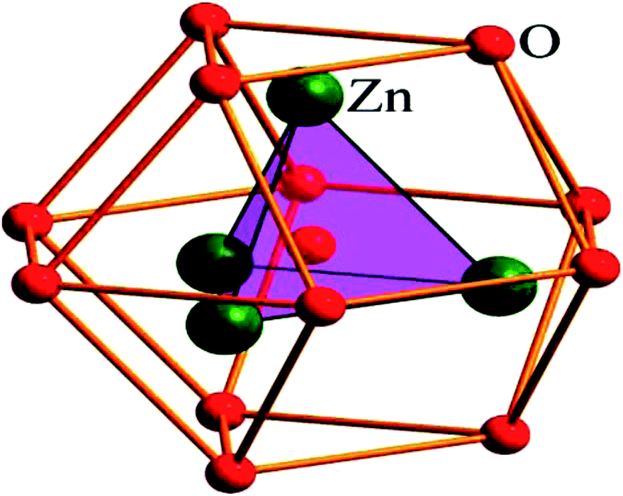
The atomic packing factor (APF) is the fraction of volume in a crystal structure that is occupied by atoms. It is dimensionless and is always less than unity. Pure and Mn doped ZnO nanoparticles have the wurtzite structure, with HCP (hexagonal close-packed) arrangement. HCP has two types of voids in the crystal structure, i.e. tetrahedral and octahedral voids.
After SHI irradiation of pure and Mn doped ZnO, the values of APF were reduced with Ni7+ ions irradiation, which introduced the presence of voids. Reshak et al.46 reported that the space group of the ZnO sample is P63mc for this structure, which has six octahedral voids in the 2a sites with coordinate (0 0 3/4) geometry. The shortest distance between the oxygen atoms from the octahedral voids is 2.28 Å, as shown in Fig. 2.
The APF of the materials was evaluated using the following formula:47
 | (5) |
It was observed that the value of APF slightly decreased after SHI irradiation, which may be due to the enhancement of voids in the samples. The APF of bulk hexagonal ZnO materials is about 74%, but in our case, the APF of ZnO nanoparticles is nearly 75% for the pristine sample, and is 74.5% for the irradiated sample, in a hexagonal structure. This means that the APF in nanocrystals is slightly larger than that of bulk materials, due to the effect of SHI irradiation on the samples.
The surface area to volume ratio of the nanoparticles has a significant effect on their properties. Firstly, thin films have a relatively larger surface area when compared to the same volume of the material. The surface to volume ratio was calculated by using the following equation:48
 | (6) |
| Sample | Fluence (ions per cm2) | Lattice parameter | Crystallite size (nm) | APF | X-ray density (gm cm−3) | S/V | |
|---|---|---|---|---|---|---|---|
| a (nm) | c (nm) | ||||||
| x = 0.00 | Pristine | 0.3271 | 0.5215 | 23.57 | 0.767 | 5.691 | 0.050 |
| Irradiated 5 × 10¹³ ions per cm2 | 0.3268 | 0.5209 | 24.41 | 0.761 | 5.638 | 0.043 | |
| x = 0.05 | Pristine | 0.3269 | 0.5206 | 27.64 | 0.758 | 5.699 | 0.039 |
| Irradiated 5 × 10¹³ ions per cm2 | 0.3253 | 0.5156 | 32.24 | 0.757 | 5.596 | 0.029 | |
Photoluminescence (PL) study
Photoluminescence is a sensitive method for examining the sample quality, especially its optical properties. Further information about the optical properties of pure and Mn doped ZnO can be obtained from PL spectra, in addition to information about the crystal modality, structural defects such as oxygen vacancy, Zn interstitials and surface properties of particles. ZnO is a strongly luminescent material that is used with several polymers. The PL spectral studies before and after SHI irradiation using nickel ion irradiation with a high energy beam of 160 MeV of undoped and 5% Mn doped ZnO thin films were recorded in the wavelength range of 400 to 900 nm. Fig. 4 shows the PL spectra of the composite formed with the glass substrate, with a peak around 3.25 eV, attributed to the band-edge excitonic transition of ZnO. A broad emission band covers the green–red spectral region from 500 nm to 750 nm. Y. Hao et al.49 reported PL spectra with UV emission and defect-related blue emission, but in our case it was noticed that in the visible range for all samples, the green–red emission presents a much higher intensity than the blue, indicating that yellow light is predominant in the white light emission. In pure ZnO thin films, the irradiated sample has increased wavelength as compared to the pristine pure ZnO, and the same trend was observed in 5% Mn doped ZnO thin films. On performing Gaussian deconvolution of the PL spectra, it was observed that an intense, broad, green band at 506 nm appeared in the PL spectra, which can be attributed to deep level emission caused by impurities and structural defects inherent in pristine ZnO nanoparticles, such as oxygen vacancies, zinc interstitials, etc., and there was a less intense blue emission near 506 nm, because of intrinsic defects such as oxygen and zinc interstitials.50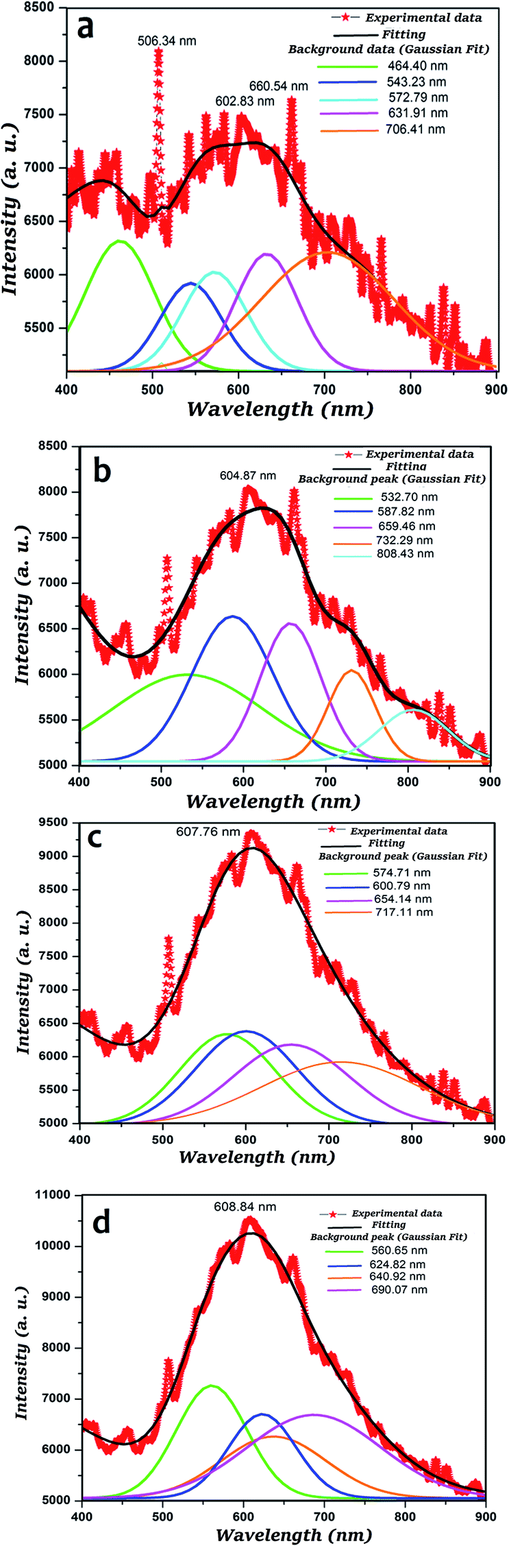 | ||
| Fig. 4 PL spectra of (a) pristine ZnO thin film, (b) irradiated ZnO thin films, (c) pristine 5% Mn doped ZnO thin film, (d) irradiated 5% Mn doped ZnO thin films. | ||
Herein, for pristine ZnO the sample exhibits a UV emission peak at 464.40 nm and five defect peaks, which correspond to green emissions near 543 and 572 nm and an orange band at 630 nm, and red emission near 706.41 nm in the PL spectra with Gaussian fitting. The main peak at 602.83 nm could be ascribed to the transition occurring from Zn interstitials to the valence band, and it may be the result of the singly ionized oxygen vacancy.51
The ZnO sample irradiated with NI7+ SHI ions had an enhancement in the wavelength, into the visible and infrared range for all spectra. Apart from the two common peaks, the other two emission peaks observed in the orange and the red regions are the focus of attention. The orange band at a wavelength of around 604.87 nm was attributed to either the presence of excess local oxygen or structural imperfections.52 Enhancement of the wavelength after SHI irradiation was due to cascade formation in the inner core of the samples; this cascade changed the electron position and was observed in the infrared region. The fourth and fifth bands were Gaussian fitted, observed in the infrared region at wavelengths of 732.29 nm and 808.43 nm, respectively. The sputtered ZnO films exhibited n-type conductivity, which led to red and IR emission bands.53 It is believed that this emission resulted from the formation of native defects. The origin of this band is still ambiguous and needs to be further investigated.
The 5% Mn doped ZnO sample had four peaks, at 574.71, 600.79, 654.14 and 717.11 nm, which were fit to the Gaussian model. Without irradiation, the spectra of the 5% Mn doped ZnO thin films were in the visible and infrared regions as compared to pure ZnO samples. It was observed that the enhancement of intensity as well as wavelength, are due to the effect of Mn doping in the ZnO. The peak at 607.76 nm, corresponding to the orange region, was enhanced as compared to the pure ZnO thin films; it is clearly evidenced that the Mn content increases the wavelength of the samples.
To perform Gaussian deconvolution of the PL spectra of MnxZn1–xO (x = 0.05) samples irradiated with Ni7+ SHI ions, the behavior of visible band components depending on x should be clarified. For this purpose, the PL spectra of the un-doped and Mn doped ZnO samples were measured under excitation by light with λ = 320 nm, corresponding to band-to-band absorption, and were analyzed. Four bands were observed, 560.65 nm, corresponding to green emission, 624.82 and 640 nm corresponding to orange emission and 690.07 nm corresponding to red emission. It is clear that the all spectra were observed the visible region, but after SHI irradiation, the intensity changed as well as the region of the band spectra, due to the cascade formation in the materials.
Raman spectra
The Raman spectra of pure and 5% Mn doped ZnO thin films in the range 200–800 cm−1 are shown in Fig. 5. The pure ZnO thin films have wurtzite structure with space symmetry C46v (P63mc), found using the Halford method.54 The optical phonon irreducible representation is given by eqn (7).| Γopt = A1 + 2B1 + E1 + 2E2 | (7) |
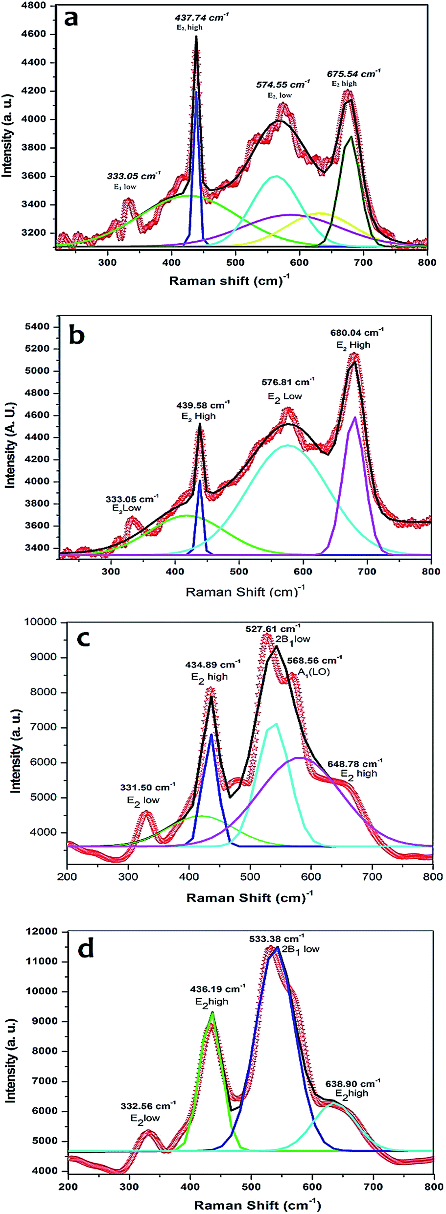 | ||
| Fig. 5 The Raman spectra of (a) pristine ZnO, (b) irradiated ZnO, (c) pristine 5% Mn doped ZnO, (d) irradiated 5% Mn doped ZnO thin films. | ||
In irradiated pure ZnO thin films, the four Raman modes, 333.05, 439.58, 576.81 and 680.04 cm−1, were observed. The observed phonon mode is (E2, high) 436 cm−1, shifted towards higher wave number, 439.58 cm−1, with respect to pristine ZnO, as is usual for nanocrystals.58 The spectra of the irradiated films show that the intensity of the E2 high (680.04 cm−1) mode increases drastically upon irradiation at 1 × 1013 cm2 fluence, due to the high energetic ions interacting with the electrons in the samples, due to the change in the geometry as well as the structure of the sample.
Mn doped ZnO pristine samples showed peaks, in the Gaussian fitted mode, at 331.50, 434.89, 527.61 and 568.56 cm−1. The peak wavelength decreases of Mn doped ZnO samples as compared to the pure ZnO sample but intensity enhances due to the effect of Mn doping. It evidences that ion irradiation induces a microscopic structural disorder and gives rise to local distortions in the lattice. The Raman mode at 434.89 cm−1 reveals the vibration of the oxygen atoms in the ZnO lattice. The 527.61 cm−1 mode was observed, which belongs to the 2B1 low mode, for the B-modes. In contrast, one sublattice is essentially at rest, while in the other sublattice, the neighboring atoms move in opposite directions. In the case of the B1 (low) mode, the heavier Zn sublattice is distorted, while the B1 (high) involves the lighter O sublattice; no net polarization is induced by the B modes, thus, the A and B modes may be classified as one polar and two non-polar modes.
After Ni7+ SHI irradiation, the 5% Mn doped ZnO thin film showed drastic changes in intensity, as well as wavelength of the Raman mode. In the irradiated sample, the 568.56 cm−1 peak disappeared after irradiation at a fluence of 1 × 10¹³ ions per cm2. It was observed that the Mn content doped in the ZnO thin films decreased the wavelength, but after SHI irradiation, it was increased, due to the effect of cascade formation in the materials. When high energetic ions were passed through the samples latent tracks were formed owing to the rearrangement of the electron positions. These latent tracks are responsible to change the internal structure of the samples. After SHI irradiation of pure and 5% Mn doped ZnO thin films, a shift in the Raman mode towards the higher wavelength was observed, due to the effect of SHI irradiation.
I–V measurements
Electrical properties of all films, i.e., pristine and irradiated films, were studied by measuring current as the function of voltage. The plots are shown in Fig. 6. S. P. Pandey59 reported an increase in the resistivity after irradiation, but in our case, the pristine and irradiated Mn doped ZnO samples revealed an enhancement in the conductivity after SHI irradiation. Hence, one could assume that the decrease in resistivity might be due to the creation of oxygen vacancies (VO) and interstitial zinc (Zn), during the irradiation with swift heavy ions. A decrease in resistivity was observed, which could be attributed to the beginning of the hopping conduction of ion beams, producing defects. The conductivity is mainly controlled by the counterbalance between the presence of oxygen vacancies, which act as doubly charged electron donors and structural (Zn) defects, which influence the carrier mobility within the thin film. The same trend was observed for the 5% Mn doped ZnO sample. The pristine 5% Mn doped ZnO sample had increased conductivity as compared to the pure ZnO thin film, but after SHI irradiation it was drastically enhanced to 2 × 10⁻⁶ amperes. This provides evidence that the effect of SHI irradiation changes the conductivity, due to the irradiation-induced thermal annealing of the defects and hence an improvement in the crystallinity at the interface of the Mn doped ZnO thin film. The irradiation induced increment in electrical conductivity of the zinc oxide thin film is due to the scattering of charge carriers from defects and grain boundaries, and widening of the band gap, and breaks some of the covalent bonds in the ZnO semiconductor, thus generating free electron–hole pairs. The irradiation sensing study of pristine and irradiated pure and 5% Mn doped ZnO thin film were studied by a two probe I–V measurement system. The irradiation sensor efficiency (Re) was calculated by the following equation:60
 | (8) |
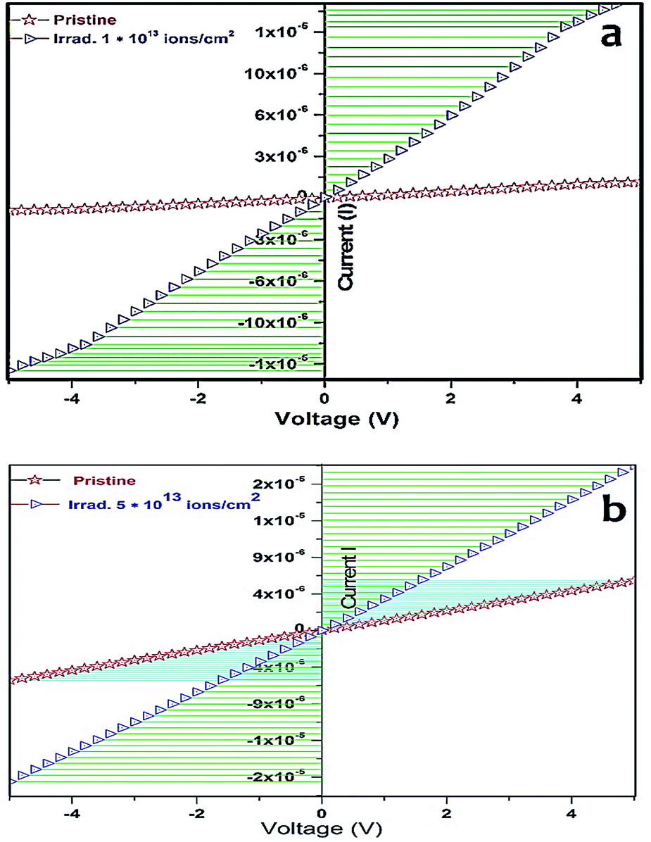 | ||
| Fig. 6 I–V characteristics of (a) pristine pure and 5% Mn doped ZnO, (b) irradiated pure and 5% Mn doped ZnO thin films. | ||
The irradiation responsibility (Rr) was calculated by the equation60
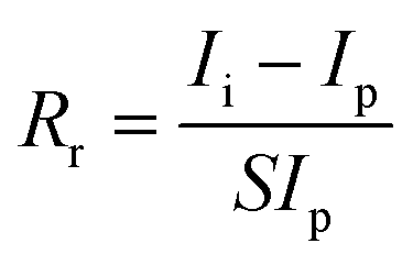 | (9) |
AFM study
Atomic force microscopy (AFM) scans of the surfaces of these films were carried out to determine the changes in surface morphology of the films. 2D and 3D AFM images of both pristine and irradiated samples clearly outline the change in surface morphology and roughness, due to the swift heavy ion beam irradiation as shown in Fig. 7. The AFM image of the pristine sample showed a typical three dimensional growth structure with irregular grains of nearly the same sizes and a surface roughness (RMS) of 89.96 nm.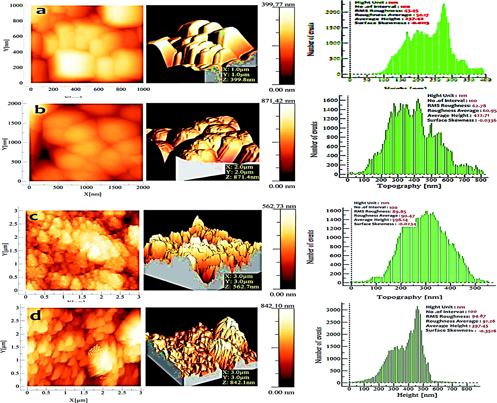 | ||
| Fig. 7 AFM images of (a) pristine ZnO, (b) irradiated ZnO, (c) pristine 5% Mn doped ZnO, (d) irradiated 5% Mn doped ZnO thin films. | ||
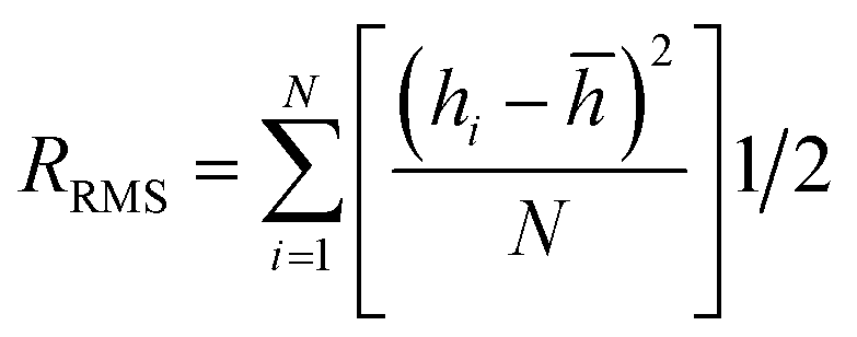
The root-mean-square roughness (RMS) has been calculated by using the formula60
 | (10) |
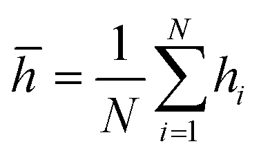
![[h with combining macron]](https://www.rsc.org/images/entities/i_char_0068_0304.gif) represents the profile mean value of the surface, and N represents the number of data points in the analyzed profile. Thus, the standard roughness or the arithmetic average roughness height represents the arithmetic mean of the deviations in height from the profile mean value, where the profile mean value is calculated using following equation:60
represents the profile mean value of the surface, and N represents the number of data points in the analyzed profile. Thus, the standard roughness or the arithmetic average roughness height represents the arithmetic mean of the deviations in height from the profile mean value, where the profile mean value is calculated using following equation:60
 | (11) |
In comparison to pristine and irradiated ZnO, the root-mean-square (RMS) roughness of the pristine film was 43.45 nm, which increased to 62.78 nm at 1 × 10¹³ ions per cm2 fluence. The same trend was observed in Mn doped ZnO samples, which increased the RMS roughness for the pristine sample to 89.85 nm, and the irradiated sample to 94.87 nm, due to the defect formation in the sample after SHI irradiation; thus, the roughness of the films is affected by the electronic excitation induced by SHI irradiation. The multiple parameters of a sample are described by factors that give information about statistical average values, the shape of the histogram heights and other extreme properties.
It was also determined that the grain size of pure and Mn doped ZnO thin films increased after the Ni7+ SHI irradiation.
Surface skewness was used to measure the symmetry of the variations of a surface about the mean line, and is more sensitive to occasional deep valleys or high peaks. Skewness illustrates the load carrying capacity, porosity, and characteristics of nonconventional machining processes. Negative skew is a criterion for a good bearing surface. Usually, surface skewness is used to distinguish two profiles of the same average roughness values, but of different shapes.61 For a pristine sample of pure ZnO, the surface skewness value was increased, compared to the irradiation thin film. The same results were observed for 5% Mn doped ZnO samples; the value of surface skewness was increased, due to the increase in porosity in the sample after SHI irradiation. The changes in size and shape of the grains at higher fluence are due to the high density of defects induced by the high electronic excitation energy of Ni+7 ion irradiation, and the major grain growth also yields an increase in the surface roughness.
Conclusions
Thin films of pure and Mn doped ZnO have been synthesized by using the dip coating technique. XRD data indicate the successful incorporation of Mn into the ZnO lattice without any secondary phase. The pristine and Mn doped ZnO thin films were irradiated by using a 160 MeV Ni7+ ion beam at a fluence of 1 × 10¹³ ions per cm2. The crystallite size increased after the SHI irradiation of pure and Mn doped ZnO thin films. The surface area to volume ratio and APF value were slightly decreased after SHI irradiation, due to the enhancement of voids in the samples. Photoluminescence studies revealed increased luminosity of pure and Mn doped ZnO thin films; these samples were irradiated with Ni7+ ions of 160 MeV energy, after which the luminosity of the samples was enhanced. The observed changes in the E2, high, E2, low and A1 (LO) Raman modes are consistent with the creation of defects, vacancies and interstitials in the zinc and oxygen sublattices. Raman measurements revealed the appearance of forbidden modes B1 (low) after doping 5% Mn in ZnO, due to relaxation of the Raman selection rules associated with the breakdown of translational crystal symmetry. I–V characteristics revealed that the enhancement in the conductivity after SHI irradiation was due to the ion–electron interaction. AFM data showed a significant difference after SHI irradiation of the samples, where the film surface exhibited a higher roughness and clear grains.Acknowledgements
The authors are grateful to IUAC, New Delhi for providing the ion beam irradiation facilities through Project No. IUAC/XIII.3A/UFR No. 52309 and Prof. S. S. Shah for his continuous encouragement.References
- B. Pelaz, S. Jaber, D. de Aberasturi, V. Wulf, T. Aida, J. de la Fuente, J. Feldmann, H. Gaub, L. Josephson, C. Kagan, N. Kotov, L. Liz-Marzán, H. Mattoussi, P. Mulvaney, C. Murray, A. Rogach, P. Weiss, I. Willner and W. Park, ACS Nano, 2012, 6, 8468–8483 CrossRef CAS PubMed.
- A. Andrews, A. Schepartz, J. Sweedler and P. Weiss, J. Am. Chem. Soc., 2014, 136, 1–2 CrossRef CAS PubMed.
- P. Weiss, ACS Nano, 2015, 9, 3397–3398 CrossRef CAS PubMed.
- C. Chey, H. Alnoor, M. Abbasi, O. Nur and M. Willander, Phys. Status Solidi A, 2014, 211, 2611–2615 CrossRef CAS.
- S. Kumar, Y. S. Katharria, Y. Batra and D. Kanjilal, J. Phys. D: Appl. Phys., 2007, 40, 6892–6897 CrossRef CAS.
- P. Boisseau and B. Loubaton, C. R. Phys., 2011, 12, 620–636 CrossRef CAS.
- F. Adams and C. Barbante, Spectrochim. Acta, Part B, 2013, 86, 3–13 CrossRef CAS.
- Z. Wang, Science, 2006, 312, 242–246 CrossRef CAS PubMed.
- S. Chen, W. Chen and I. Buyanova, Phys. Rev. B: Condens. Matter Mater. Phys., 2011, 83, 245212 CrossRef.
- C. Ronning, P. Gao, Y. Ding, Z. Wang and D. Schwen, Appl. Phys. Lett., 2004, 84, 783 CrossRef CAS.
- M. Willander, P. Klason, L. Yang, S. Al-Hilli, Q. Zhao and O. Nur, Phys. Status Solidi C, 2008, 5, 3076–3083 CrossRef CAS.
- P. Solanki, A. Kaushik, V. Agrawal and B. Malhotra, NPG Asia Mater., 2011, 3, 17–24 CrossRef.
- H. Raval and J. Gohil, Int. J. Nucl. Desalin., 2010, 4, 184 CrossRef CAS.
- J. Iqbal, X. Liu, A. Majid and R. Yu, J. Supercond. Novel Magn., 2010, 24, 699–704 CrossRef.
- S. Singh, K. Barick and D. Bahadur, J. Mater. Chem. A, 2013, 1, 3325 CAS.
- S. F. Adams and C. Barbante, Spectrochim. Acta, Part B, 2013, 86, 3–13 CrossRef.
- M. El-Hilo and A. Dakhel, J. Magn. Magn. Mater., 2011, 323, 2202–2205 CrossRef CAS.
- S. Yılmaz, M. Parlak, Ş. Özcan, M. Altunbaş, E. McGlynn and E. Bacaksız, Appl. Surf. Sci., 2011, 257, 9293–9298 CrossRef.
- H. Yang, C. Zhang, X. Shi, H. Hu, X. Du, Y. Fang, Y. Ma, H. Wu and S. Yang, Biomaterials, 2010, 31, 3667–3673 CrossRef CAS PubMed.
- Y. Wang, Q. Zhao, N. Han, L. Bai, J. Li, J. Liu, E. Che, L. Hu, Q. Zhang, T. Jiang and S. Wang, Nanomedicine: Nanotechnology, Biology and Medicine, 2015, 11, 313–327 CrossRef CAS PubMed.
- P. Boisseau and B. Loubaton, C. R. Phys., 2011, 12, 620–636 CrossRef CAS.
- M. Swierczewska, G. Liu, S. Lee and X. Chen, Chem. Soc. Rev., 2012, 41, 2641–2655 RSC.
- S. Su, W. Wu, J. Gao, J. Lu and C. Fan, J. Mater. Chem., 2012, 22, 18101–18110 RSC.
- T. Kundu, S. C. Sahoo and R. Banerjee, Cryst. Growth Des., 2012, 12, 2572–2578 CAS.
- R. P. Singh, A. Tiwari, J. W. Choi and A. C. Pandey, Biological approach of Zinc Oxide Nanoparticles Formation and its Characterization, Bentham Science Publishers, 2012, vol. 3, pp. 41–50 Search PubMed.
- F. Santiago, K. A. Boulais, A. R. Keller, V. H. Gehman Jr and K. J. Long, Proc. SPIE, 2009, 7343, 73430 CrossRef.
- Y. Liu, Y. Li and H. Zeng, J. Nanomater., 2013, 196521 Search PubMed.
- M. G. Tsoutsouva, C. N. Panagopoulos, D. Papadimitriou, I. Fasaki and M. Kompitsas, Mater. Sci. Eng., B, 2011, 176, 480–483 CrossRef CAS.
- M. Smirnov, C. Baban and G. I. Rusu, Appl. Surf. Sci., 2010, 256, 2405–2408 CrossRef CAS.
- F. E. Ghodsi and H. Absalan, Acta Phys. Pol., A, 2010, 118, 120–129 CrossRef.
- J. G. Lu, T. Kawaharamura, H. Nishinaka, Y. Kamada, T. Ohshima and S. Fujita, J. Appl. Phys., 2007, 229, 1–10 Search PubMed.
- W. Gao and Z. Li, Ceram. Int., 2011, 30(7), 1155–1159 CrossRef.
- M. Smirnov, C. Baban and G. I. Rusu, Appl. Surf. Sci., 2010, 256, 2405–2408 CrossRef CAS.
- S. Hasim, M. Hamid, R. Shamsudin and A. Jalar, J. Phys. Chem. Solids, 2009, 70, 1501–1504 CrossRef.
- D. Wu, Z. Huang, G. Yin, Y. Yao, X. Liao, D. Han, X. Huang and J. Gu, CrystEngComm, 2010, 12, 192–198 RSC.
- A. Bauer, M. Godon, J. Carlier, Q. Ma and R. H. Tipping, Absorption by H2O and H2O-N2 mixtures at 153 GHz, J. Quant. Spectrosc. Radiat. Transfer, 1993, 50(5), 463–475 CrossRef CAS.
- J. S. Dunlop, D. H. Hughes, S. Rawlings, S. A. Eales and M. J. Ward, Nature, 1994, 370, 347–349 CrossRef.
- V. Sisodia and I. Jain, Bull. Mater. Sci., 2004, 27, 393 CrossRef CAS.
- S. K. Neogi, S. Chattopadhyay, A. Banerjee, S. Bandyopadhyay, A. Sarkar and R. Kumar, J. Phys.: Condens. Matter, 2011, 23, 205801 CrossRef CAS PubMed.
- H. Khawal, U. Gawai, K. Asokan and B. Dole, RSC Adv., 2016, 6, 49068–49075 RSC.
- K. Jacob, S. Raj and L. Rannesh, Int. J. Mater. Res., 2007, 98, 776–779 CrossRef CAS.
- H. A. Khawal, N. D. Raskar, U. P. Gawai and B. N. Dole, AIP Conf. Proc., 2016, 20431 CrossRef.
- S. Som, S. Das, S. Dutta, M. Pandey, R. Dubey, H. Visser, S. Sharma and S. Lochab, J. Mater. Sci., 2015, 51, 1278–1291 CrossRef.
- A. Sahai and N. Goswami, Phys. E, 2014, 58, 130–137 CrossRef CAS.
- H. A. Khawal, U. P. Gawai, M. R. Bodke, K. Asokan and B. N. Dole, Bionano Frontier, 2015, 8(3), 129–131 Search PubMed.
- A. Reshak, J. Ebothe, A. Wojciechowski, W. Kuznik and A. Popeda, Physica E: Low-dimensional Systems and Nanostructures, 2010, 42, 1769–1771 CrossRef CAS.
- V. Mote, J. Dargad, Y. Purushotham and B. Dole, Ceram. Int., 2015, 41, 15153–15161 CrossRef CAS.
- V. Mote and B. Dole, Adv. Mater. Res., 2013, 678, 234–238 CrossRef CAS.
- Y. Hao, S. Lou, S. Zhou, R. Yuan, G. Zhu and N. Li, Nanoscale Res. Lett., 2012, 7, 100 CrossRef PubMed.
- S. Sharma, R. Vyas, S. Shrivastava and Y. Vijay, Phys. B, 2011, 406, 3230–3233 CrossRef CAS.
- H. Wang, G. Wang, L. Jia, C. Tang and G. Li, J. Phys. D: Appl. Phys., 2007, 40, 6549–6553 CrossRef CAS.
- J. Kang, H. Kang, S. Pang, E. Shim and S. Lee, Thin Solid Films, 2003, 443, 5–8 CrossRef CAS.
- M. Koyano, P. QuocBao, L. ThanhBinh, L. HongHa, N. NgocLong and S. Katayama, Phys. Status Solidi A, 2002, 193, 125–131 CrossRef CAS.
- L. Duan, G. Rao, Y. Wang, J. Yu and T. Wang, J. Appl. Phys., 2008, 104, 013909 CrossRef.
- X. Zhu, H. Wu, D. Qiu, Z. Yuan, G. Jin, J. Kong and W. Shen, Opt. Commun., 2010, 283, 2695–2699 CrossRef CAS.
- S. Kumar, K. Asokan, R. Singh, S. Chatterjee, D. Kanjilal and A. Ghosh, RSC Adv., 2014, 4, 62123–62131 RSC.
- O. Lupan, L. Chow, L. Ono, B. Cuenya, G. Chai, H. Khallaf, S. Park and A. Schulte, J. Phys. Chem. C, 2010, 114, 12401–12408 CAS.
- B. Kharroubi, R. Baghdad, A. Abdiche, M. Bousmaha, M. Bousquet, A. Zeinert, M. El Marssi, K. Zellama and S. Hamzaoui, Phys. Scr., 2012, 86, 015805 CrossRef.
- S. P. Pandey, Am. J. Mater. Sci. Technol., 2012, 2(6), 215–220 CrossRef.
- A. Srivastava and J. Kumar, AIP Adv., 2011, 1, 032153 CrossRef.
- M. Ulmeanu, A. Serghei, I. Mihailescu, P. Budau and M. Enachescu, Appl. Surf. Sci., 2000, 165, 109–115 CrossRef CAS.
Footnote |
| † Electronic supplementary information (ESI) available: Ion collision, ion recoil distribution, energy loss of target phonon and energy loss of vacancy production plots are shown in Fig. 1. Table 1 shows the lattice binding energy, surface binding energy and displacement energy of ZnO nanoparticles are calculated by TRIM software. See DOI: 10.1039/c7ra01809f |
| This journal is © The Royal Society of Chemistry 2017 |