DOI:
10.1039/C7RA04821A
(Paper)
RSC Adv., 2017,
7, 29599-29605
Atomic structure, electronic properties and generalized stacking fault energy of diamond/c-BN multilayer
Received
29th April 2017
, Accepted 1st June 2017
First published on 7th June 2017
Abstract
The atomic structures, electronic properties and generalized stacking fault (GSF) energies of the diamond/c-BN multilayer are investigated systematically with first-principles calculations. A total of twelve interfacial structures are considered, encompassing two c-BN terminations, each of which involves two diamond terminations and three stacking sequences. We identify two stable interfacial structures, where the stacking sequence near the interface is identical to that in bulk diamond, implying a smooth transition across the interface. By using several analytical techniques, we find that the interfacial bonds are primarily of a mixed covalent-ionic nature, and the covalency stems from the sp3 hybridization between interfacial C sp states and B sp states. The shapes of the GSF energy curves for the interfaces are similar to those for bulk diamond and c-BN, albeit that the unstable GSF energies for the former are smaller than those for the latter. The GSF energies of the slip planes near the interface alter remarkably due to the interfacial effect, meaning that they are dependent on the slip systems.
1. Introduction
Ultrahard materials have been widely used in many fields, such as cutting and polishing tools, aerospace structural components, high power and high frequency electronic devices.1 Diamond is currently the hardest material, but its application may be limited by some of its inherent shortcomings.2 Compared with diamond, cubic boron nitride (c-BN) possesses a higher thermal and chemical stability and is considered as an ideal coating material for cutting tools. However, c-BN has a lower Vickers hardness than diamond.3
Searching for materials that are harder and more stable than diamond for practical needs has attracted increasing attention in past years, and several methods have already been reported for this purpose.4,5 It is known that boron, carbon, and nitrogen atoms have a similar ionic radii and they can form sp3 hybridized bonds, indicating that the superhard B–C–N ternary and binary materials can be considered as promising alternative candidates for diamond and c-BN. Both theoretical and experimental studies have indicated many of such materials with high hardness and excellent thermal stability, including BC2N, BC4N, BC6N, β-C3N4, BC3 and BC5.6–10 However, in terms of the Hall–Petch relation, the hardness of a nanocrystalline material increases with the decrease of its grain size. In particular, the nanoscale twin boundaries can act as regular grain boundaries.11 For example, it has been reported that nanotwinned (nt) diamond and c-BN possess an ultrahigh Vickers indentation hardness, exceeding 200 and 100 GPa (twice that of single-crystal structure), respectively, as their twin thicknesses are reduced to a few nanometers (∼3.8 nm for nt c-BN and ∼5 nm for nt diamond).12,13 Theoretically, Li et al.14 found that bond rearrangement at twin boundary can remarkably enhance indentation shear strength in nt c-BN under indentation compression and shear strains. Huang et al.15 applied molecular dynamics simulations for the responses of c-BN films under nanoindentation, and found that during the indentation, plastic deformation of c-BN is can mainly be attributed to stress-induced slips of dislocations along {111}<110> orientations. In addition, Wang et al.16 reported the synthesis and characterization of transparent bulk diamond/c-BN alloy, and showed that the alloy has a superior chemical inertness over the polycrystalline diamond and a higher hardness than a single crystal.
By introducing layered interfaces into multilayer composites, mechanical properties of materials could be greatly improved, especially as the layer thickness reaches nanometer level.17 For instance, hardness of diamond(111)/c-BN(111) nanomultilayer composites can be increased to over 80 GPa while maintaining low compressibility, high thermal stability, and p-type semiconductivity.18 Recently, an epitaxial diamond/c-BN heterojunction has been produced using a temperature gradient method, and a kind of heterointerface was found to be accommodated by a lattice mismatch, which consists of a network with continuous stacking fault arranged by hexagonal dislocation loops.19 For such composites, although their interfacial structure can be experimentally observed, it remains difficult to make clear the effects of the interfaces on mechanical properties of the composites due to the variety of interfacial structures formed in practical deposition and to the complex atomic structures and their interactions. In addition, it is known that plastic deformation and its associated nucleation, glide and transmission of dislocations are affected by interfaces,20 rendering a systematic atomistic investigation of the diamond/c-BN interface in the multilayered composites timely and important.
First-principles calculation can serve as an effective means to investigate mechanical properties and atomic and electronic structures of an interface.21–23 In this article we apply first-principles calculations to study the possible interfaces in diamond and c-BN multilayers with a special focus on atomic stacking sequences and electronic states at the interfaces. The generalized stacking fault (GSF) energies of the likely slip systems are also calculated to probe the interfacial effects on mechanical properties of the multilayer composites.
2. Calculation details
Vienna ab initio simulation package (VASP) within the framework of density functional theory (DFT) was applied in our calculation. The generalized gradient approximation by Perdew and Wang (GGA-PW91)24 was adopted to describe the exchange-correlation functional. The electron-ion core interactions were described using the pseudo-potentials of carbon, boron and nitrogen atoms with the electronic configurations of 2s22p2, 2s22p1, and 2s22p3, respectively. Single-particle Kohn–Sham wave function25,26 was extended using the plane waves with a cut-off energy of 500 eV and sampling of irreducible edge of Brillouin zone was performed with a regular Monkhorst–Pack scheme27 for all calculations. We used 11 × 11 × 11 k-point meshes for bulk calculations and 9 × 9 × 1 k-point meshes for calculations of adhesion or GSF energies. A vacuum of 15 Å was embedded into the supercell to avoid the interaction between the slab and its periodic images in the calculation of GSF energies. In all relaxations, total energy was converged to less than 10−5 eV and the Hellmann–Feynman force on each atom was set as 0.05 eV Å−1.
Adhesion energy (Wad) depended sensitively on atomic species and electronic structure of the atoms at an interface, which is the key to predict mechanical properties of an interface. Wad was defined as the energy required to break down the interfacial bonds and separate the interface into two free surfaces, which could be calculated by28
| | |
Wad = (Ediamond + Ec-BN − Eslab)/A,
| (1) |
where
Ediamond,
Ec-BN, and
Eslab were the total energy of the isolated relaxed diamond, c-BN and diamond/c-BN slab with interface, respectively, and
A was the interface area. The GSF energy, which was considered a perfect crystal cutting across a plane into two parts and subjected to a relative displacement
f and then rejoined, was usually used to measure nonelastic deformation, especially for dislocation glide and twinning. The GSF energy could be calculated by
22where
Ef and
E0 were the total energy of the supercell with and without a stacking fault.
A was the stacking fault area. To obtain the total energy with a stacking fault (
Ef), the atomic positions perpendicular to the shear displacement plane were fully relaxed, while those in the direction parallel to the slip plane were fixed to maintain stacking fault during relaxation after a relative displacement.
3. Results and discussion
3.1 Structures and properties of interfaces
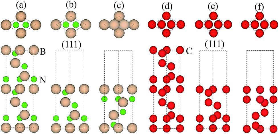
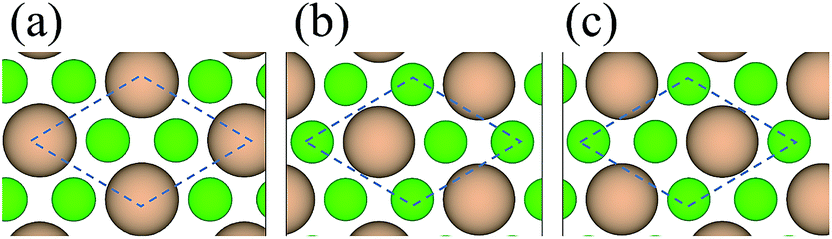
3.1.1 Adhesion energy. Table 1 compares our calculated results with the published works for both bulk diamond and c-BN, where a good consistence is achieved,29–31 validating the use of our calculation methodology to describe this system. Since the orientation relationship between diamond and c-BN is (111)diamond‖(111)c-BN and [1![[1 with combining macron]](https://www.rsc.org/images/entities/char_0031_0304.gif) 0]diamond‖[10]c-BN19 and the B–C bonds are observed at the diamond/c-BN interfaces,19,32 we consider the B-terminated c-BN only here. On the other hand, there are two types of stacking pattern in diamond structures, shuffle- and glide-set. Hence, two types of terminations of c-BN at (111) interfaces are established, denoted with B1 (Fig. 1(b)) and B2 (Fig. 1(c)). Similarly, two stacking modes in diamond (111) are also taken into consideration, as denoted with C1 (Fig. 1(e)) and C2 (Fig. 1(f)). In addition, there are three stacking sequences: interfacial C atoms of diamond are located (i) on the top surface atoms (OS) of c-BN (Fig. 2(a)), (ii) above the hollow site (HS) (Fig. 2(b)), and (iii) above the second-layer atoms (SS) (Fig. 2(c)). As a consequence, a total of 12 interfacial geometries are considered, which can be divided into two groups: B1 and B2. To satisfy the need of periodic boundary conditions, lattice constant of c-BN is shrunken by 1.20% to match that of diamond.
0]diamond‖[10]c-BN19 and the B–C bonds are observed at the diamond/c-BN interfaces,19,32 we consider the B-terminated c-BN only here. On the other hand, there are two types of stacking pattern in diamond structures, shuffle- and glide-set. Hence, two types of terminations of c-BN at (111) interfaces are established, denoted with B1 (Fig. 1(b)) and B2 (Fig. 1(c)). Similarly, two stacking modes in diamond (111) are also taken into consideration, as denoted with C1 (Fig. 1(e)) and C2 (Fig. 1(f)). In addition, there are three stacking sequences: interfacial C atoms of diamond are located (i) on the top surface atoms (OS) of c-BN (Fig. 2(a)), (ii) above the hollow site (HS) (Fig. 2(b)), and (iii) above the second-layer atoms (SS) (Fig. 2(c)). As a consequence, a total of 12 interfacial geometries are considered, which can be divided into two groups: B1 and B2. To satisfy the need of periodic boundary conditions, lattice constant of c-BN is shrunken by 1.20% to match that of diamond.
Table 1 Comparison of our predicted structural parameters with the experimental and other reported resultsa
| Parameters |
Diamond |
c-BN |
| This work |
Exp.29 |
Others31 |
This work |
Exp.30 |
Others31 |
| a: lattice constant; C11, C12, C44: elastic constants; and K: bulk modulus. |
| a (Å) |
3.575 |
3.567 |
3.567 |
3.625 |
3.615 |
3.627 |
| C11 (GPa) |
1052 |
1079 |
1055 |
791 |
820 |
783 |
| C12 (GPa) |
125 |
124 |
120 |
173 |
190 |
172 |
| C44 (GPa) |
556 |
578 |
559 |
447 |
480 |
444 |
| K (GPa) |
434 |
443 |
431 |
379 |
382 |
376 |
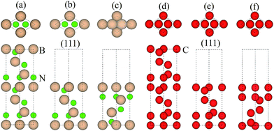 |
| | Fig. 1 Atomic structures: (a) bulk c-BN, (b) B1, (c) B2, (d) bulk diamond, (e) C1, and (f) C2. The upper parts are top views and the lower ones are side views. Only the top seven of thirteen symmetric layers are presented for each termination. | |
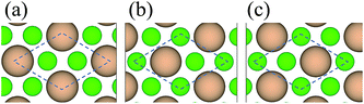 |
| | Fig. 2 Stacking sequences between diamond and c-BN: (a) OS site, (b) HS site, and (c) SS site. The c-BN proximal to interface is presented only for clarity. Dotted parallelogram outlines denote the projection of unit diamond cell in [111] direction. | |
Table 2 lists adhesion energies of all the interfaces. In the B1 case, the adhesion energy for the OS stacking sequence is larger than that for the HS and SS, and the largest Wad = 11.325 J m−2 appears in the case of C1/B1 with OS, the atomic structure of which is shown in Fig. 3(a). The stacking sequence at the interface with the largest Wad is identical to that of bulk diamond structure. In the B2 case, the C2/B2 with HS possesses the largest Wad of 18.301 J m−2, and the corresponding atomic structure is shown in Fig. 3(b). The atomic stacking sequence at this interface also retains that in the bulk diamond (or c-BN). Such stacking sequence provides a smooth transition from c-BN to diamond. It is worthy of noting that the C2/B2 with SS has an adhesion energy of 18.211 J m−2, very close to that of C2/B2 with HS. By comparing the adhesion energies of the 12 interfacial structures, we find the most stable interfaces in the B1 (Fig. 3(a)) and B2 (Fig. 3(b)) cases.
Table 2 Wad (J m−2) for the twelve interfacial structures, including two terminated structures B1 and B2 and three possible stacking sequences OS, HS and SS site
| Termination |
Stacking sequences |
| c-BN |
Diamond |
OS |
HS |
SS |
| B1 |
C1 |
11.325 |
4.907 |
2.122 |
| C2 |
11.085 |
6.507 |
4.356 |
| B2 |
C1 |
7.285 |
1.049 |
0.043 |
| C2 |
5.789 |
18.301 |
18.211 |
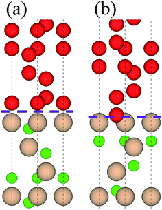 |
| | Fig. 3 Two stable interfacial atomic configurations: (a) B1 and (b) B2. Upper parts are diamond and lower parts are c-BN. Interface is denoted by dotted lines. | |
3.1.2 Local atomic structure. As shown in Fig. 3, there is a significant difference between the two types of interfaces, B1 and B2 (e.g. bond length at interface), which accounts for their distinct Wad (B2 is greater than B1 in Wad). For B1, the interfacial B–C distance is calculated as 1.655 Å, strikingly larger than 1.544 Å for bulk diamond and 1.563 Å for c-BN. The lengths of C–C and B–N bonds near to the interface are 1.551 and 1.562 Å, respectively, which deviate by 0.11 Å from that of bulk diamond and 0.09 Å from that of bulk c-BN. Such deviation is screened to less than 0.06 Å in the following layers, implying that the effect of B1 interface is rather confined. For B2, the interfacial B–C distance is 1.614 Å, smaller than that of B1. The lengths of sub-interfacial C–C and B–N bond lengths are 1.502 Å and 1.549 Å, respectively, which deviate by 0.07 Å from that of bulk diamond and 0.05 Å from that of bulk c-BN. This deviation is screened to less than 0.03 Å in the following layers, implying that the interfacial effect is localized.
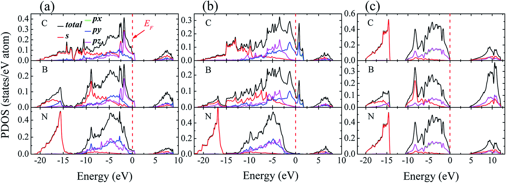
3.1.3 Electronic properties. Fig. 4 shows density of states (DOS) projected onto selected atomic layers of the two interfaces. A key feature in Fig. 4 is that the partial densities of states (PDOSs) of the interfacial C and B layers show states at Fermi level (EF) (Fig. 4(a) and (b)), indicating metallic nature at the interfaces, which vanishes in bulk diamond or c-BN (Fig. 4(c)). Such metallic behavior at the interface can be attributed to the fact that boron atoms can serving as dopants on the surface of pure diamond.33 In addition, a significant sp3 hybridization can be observed between interfacial sp states of C and sp states of B, indicating that the covalent bonds emerge at interface. It is worthwhile noting that the pz state of the entire interfacial atoms suffers a significant change in the energy range between −10 and 0 eV, which is ascribed to the hybridization between the interfacial atoms.
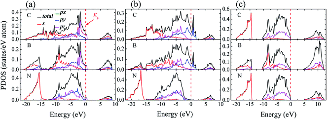 |
| | Fig. 4 Density of state (DOS) for (a) B1, (b) B2, and (c) bulk diamond and c-BN. For the multilayer, the PDOS of the first C layer in diamond part, first B layer and second N layer in c-BN part are present. The Fermi level is set to zero and represented with vertical dotted lines. | |
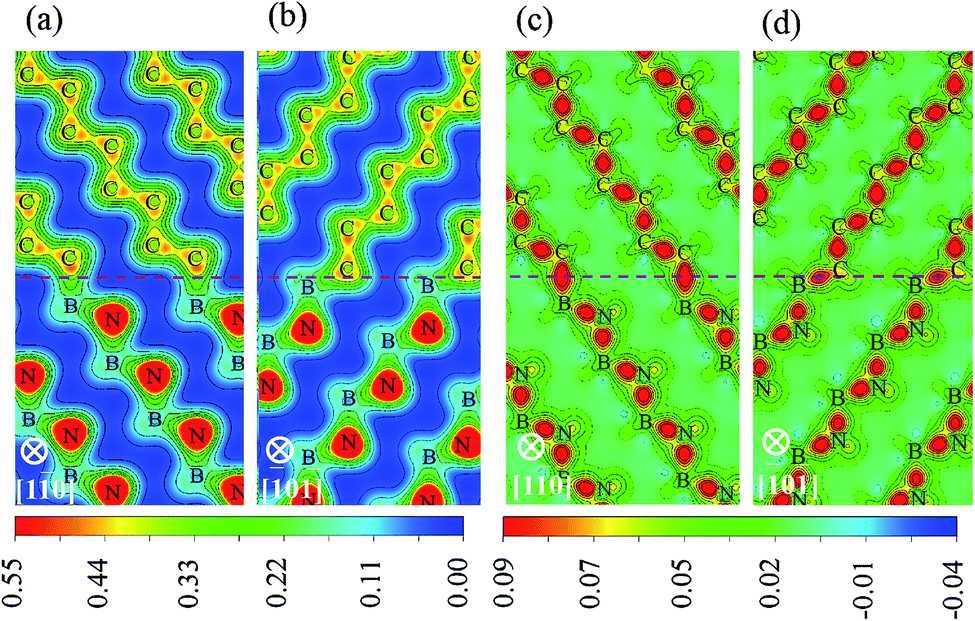
To identify the type of chemical bond at interface, the charge density distribution and its difference are calculated, as shown in Fig. 5, in which the difference of charge density is calculated by subtracting the sum of the isolated diamond and c-BN slabs from the total interface charge density. There is a significant feature in Fig. 5(a) and (b) between the charge density of bulk c-BN and that of diamond. Charge distribution around N of c-BN is approximately spherically symmetric and distorted toward the neighboring B, indicating that c-BN has mixed ionic and covalent nature. It can be seen in Fig. 5(a) and (b) that charge in diamond region is located in the bridge section between C atoms, indicative of covalent bonds only in bulk diamond. Most of charges are located along B–N bonds in the region of c-BN and along C–C bonds in the diamond area, as shown in Fig. 5(c) and (d). Interfacial C–B bonds exhibit the following characters: (i) most charges are located around C atoms, and (ii) charges around C atoms are distorted toward the neighboring B atoms and remarkably accumulated along the interfacial B–C bonds. These two observations suggest that the interfacial bonds are primarily of mixed covalent-ionic nature, which explains why the interfaces show a metallic character.
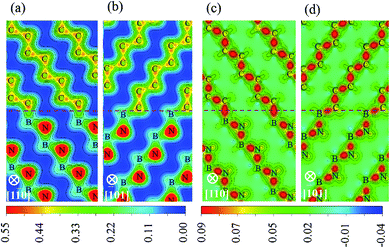 |
| | Fig. 5 Distribution of charge densities and charge density differences: charge density of (a) B1 and (b) B2, charge density difference of (c) B1 and (d) B2. The interfaces are represented with horizontal dotted lines. | |
3.2 GSF energies of interfaces
3.2.1 GSF energies of interfaces. For a crystal of diamond-structure, there exist two patterns of stacking faults on the {111} plane, glide- and shuffle-set, each of which has two types of slip directions, <110> and <112>, as shown in Fig. 6(c). It can be found that the B1 interface is of shuffle-set pattern (Fig. 6(a)), while the B2 interface can only form glide-set dislocation (Fig. 6(b)). There are two common intrinsic energy barriers, the unstable stacking fault energy (γUSF) and stable stacking fault energy (γSF), which are formally defined as maximum and minimum energies in GSF energy curves, respectively. The values of the γUSF for all the slip systems are listed in Table 3. These energy barriers are related to many factors, such as phase transition, crystal growth, plastic deformation, dislocation glides and twin interactions.34–36
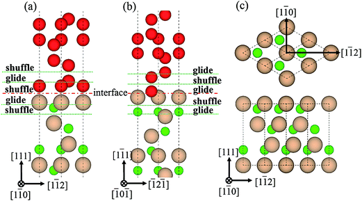 |
| | Fig. 6 Dislocations patterns, glide- and shuffle-set. (a) B1, (b) B2, and (c) two slip directions, <110> and <112>. | |
Table 3 The γUSF for the interfaces in B1 and B2, and for the bulk c-BN and diamond
| Slip systems |
B1 interface |
B2 interface |
Bulk c-BN |
Bulk diamond |
| {111}<110> shuffle |
6.995 |
— |
7.218 |
8.825 |
| {111}<112> shuffle |
9.123 |
— |
9.325 |
10.303 |
| {111}<110> glide |
— |
10.080 |
11.166 |
13.546 |
| {111}<112> glide |
— |
— |
1.893 |
12.346 |
3.413 |
13.171 |
5.285 |
13.588 |
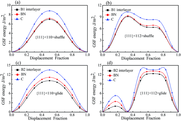
Fig. 7 shows the GSF energies of the two kinds of interfaces with displacements along <110> and <112> directions, in which the GSF energies of bulk diamond and c-BN are also presented for comparison. It can be seen that the GSF energy curves of the interfaces have a shape similar to that of bulk diamond and c-BN. For all the slip systems, the γUSF of the interfaces are almost equal to that of bulk c-BN, especially in case of shuffle-set dislocation. The shuffle-set dislocation in <110> direction possesses the minimum γUSF of 6.995 J m−2 (Fig. 7(a)), indicating that {111}<110> is the easiest direction for dislocation glide. The {111}<112> slip system for the glide-set dislocation has two values of γUSF (1.893 and 12.346 J m−2), as shown in Fig. 7(d). The existence of the lower γUSF (1.893 J m−2) indicates that resistance to the formation of twin structure in this slip system is much lower than that in bulk diamond (5.286 J m−2) and c-BN (3.413 J m−2). This also suggests that the {111}<112> slip system is easier to form partial dislocations.
 |
| | Fig. 7 The GSF energies of the interfaces B1 and B2, and of bulk C and c-BN: (a) and (b) are the B1 interface, (c) and (d) are B2 interface. | |
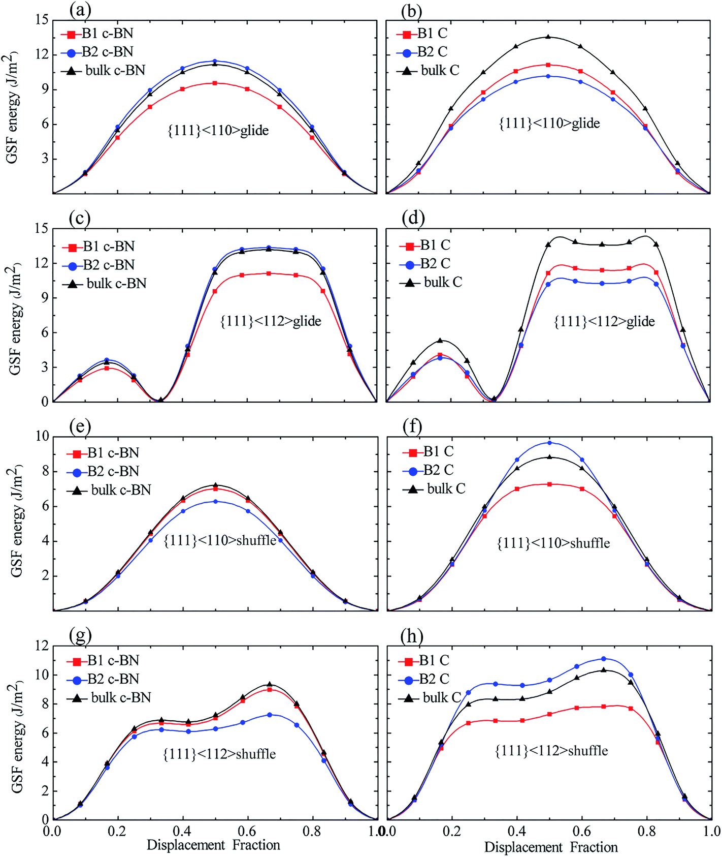
3.2.2 Effect of interfaces. Since the interfacial effects are localized in terms of atomic structure and the GSF energies of the layer far away from interface is insignificantly affected by interface, we therefore only calculate the GSF energy curves for some layers near interface in all systems, as shown in Fig. 8. The slip systems include two types of stacking pattern, glide- and shuffle-set (Fig. 6(a) and (b)), and two slip directions, <110> and <112> (Fig. 6(c)). The GSF energies of bulk diamond and c-BN are also presented for comparison. The γUSF for all the slip systems are listed Table 4. The GSF energy curves for B1 and B2 show the same trend as those for bulk materials.
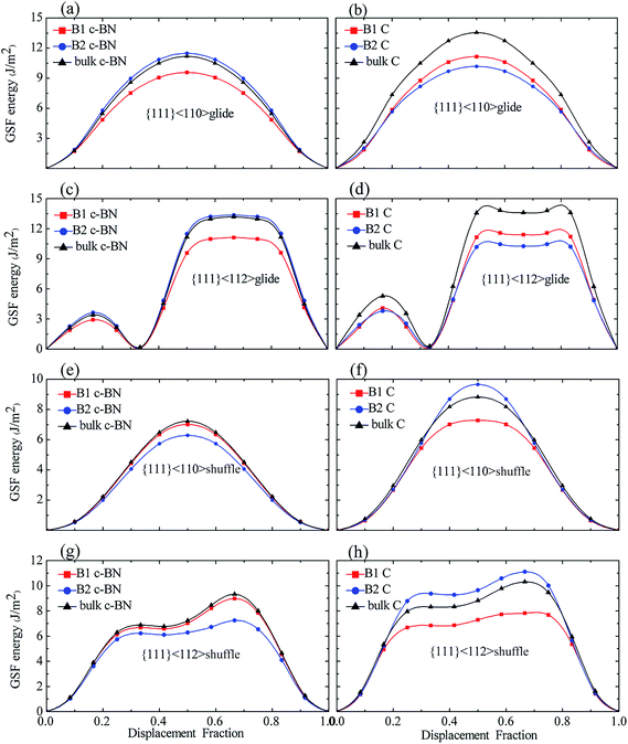 |
| | Fig. 8 The GSF energies of slip planes near the interfaces and of bulk diamond and c-BN: (a and b) {111}<110> glide, (c and d) {111}<112> glide, (e and f) {111}<110> shuffle, and (g and h) {111}<112> shuffle dislocations. The GSF energies of c-BN and diamond layer are shown on the left and right panel, respectively. | |
Table 4 The γUSF of slip layers near the interfaces in B1 and B2, and of bulk c-BN and diamond
| Slip systems |
c-BN |
Diamond |
| B1 |
B2 |
Bulk |
B1 |
B2 |
Bulk |
| {111}<110> glide |
9.566 |
11.489 |
11.158 |
11.143 |
10.173 |
13.546 |
| {111}<112> glide |
11.120 |
13.353 |
13.163 |
11.411 |
10.254 |
13.588 |
| {111}<110> shuffle |
7.012 |
6.277 |
7.218 |
7.285 |
9.652 |
8.825 |
| {111}<112> shuffle |
8.987 |
7.256 |
9.325 |
7.807 |
11.112 |
10.303 |
For the c-BN layers in {111}<110> glide-set and {111}<112> glide-set slip systems, the GSF energies of B2 are somewhat higher than those in bulk c-BN, and the B1 has the lowest γUSF. As shown in Fig. 8(a) and (c), both B1 and B2 have a low γSF in {111}<112> glide-set slip system. For the c-BN layers in {111}<110> shuffle-set and {111}<112> shuffle-set slip systems, the GSF energies of B1 are slightly smaller than those in bulk c-BN (Fig. 8(e) and (f)), the trend of which reverses as compared to the former slip systems. The B2 in {111}<110> shuffle-set slip system has the lowest γUSF of 6.277 J m−2, indicating that perfect dislocation is easy to form in this slip system. In general, for the c-BN layers, little change is found in the GSF energies between B2 in {111}<110> and {111}<112> glide-set slip systems and of B2 in {111}<110> and {111}<112> shuffle-set slip systems.
For the diamond layers in {111}<110> glide-set and {111}<112> glide-set slip systems, the GSF energies for B1 and B2 are significantly lower than that in bulk diamond, as shown in Fig. 8(b) and (d). The B2 has the lowest γUSF, and the B1 and B2 almost have the same γUSF in {111}<112> glide-set slip system. For the diamond layers in {111}<110> shuffle-set and {111}<112> shuffle-set slip systems (Fig. 8(f) and (h)), the GSF energies of B2 is higher than that of B1 and bulk diamond, while the GSF energies of B1 is less than that of bulk diamond, which differs from the former slip system in the diamond layers. For the diamond layers, the GSF energies of B2 in {111}<110> shuffle-set and {111}<112> shuffle-set slip systems increases significantly, while that for the rest decreases. Therefore, we conclude that the GSF energies of the slip planes near interface behaves differently due to the interface, meaning that they are dependent on the slip systems.
4. Conclusions
We have investigated the atomic structure, electronic properties, and generalized stacking fault energy of the diamond/c-BN multilayer systematically with first-principles calculation. A total of twelve interfacial structures are considered, encompassing two c-BN terminations, each of which involves two diamond terminations and three stacking sequences. By comparing adhesion energy, we identify two stable interfacial configurations, where stacking sequences near the interfaces are identical to those in bulk diamond, implying a smooth atomic transition across interface. Several analytic methods are applied to characterize the nature of the interfaces. The interfacial bonds are primarily of mixed covalent-ionic nature, and the covalency of interfacial bonds stems from the sp3 hybridization between the sp states of C and of B. Most charges are located around C atoms, which are distorted toward the neighboring B atoms and remarkably accumulated along the interfacial B–C bonds. Further calculation of GSF energy reveals that the shape of the GSF energy curves for the interfaces is similar to that of bulk diamond and c-BN, despite that the unstable stacking fault energies for the former are smaller than those for the latter. The GSF energies of the slip planes near interface alter differently due to interfacial effect, meaning that they rely on the slip systems.
Acknowledgements
The authors gratefully acknowledge the financial supports from National Natural Science Foundation of China (grant no. 11332013), Chongqing Graduate Student Research Innovation Project (grant no. CYB16023), and Chongqing Research Program of Basic Research and Frontier Technology (grant no. cstc2015jcyjA50008 and cstc2016jcyjA0366).
References
- R. B. Kaner, J. J. Gilman and S. H. Tolbert, Science, 2005, 308, 1268–1269 CrossRef CAS PubMed.
- J. E. Field, Rep. Prog. Phys., 2012, 75, 253–274 CrossRef PubMed.
- C. B. Samantaray and R. N. Singh, Int. Mater. Rev., 2013, 50, 313–344 CrossRef.
- Z. S. Zhao, B. Xu and Y. J. Tian, Annu. Rev. Mater. Res., 2016, 46, 383–406 CrossRef CAS.
- T. Fu, X. Peng, X. Chen, S. Weng, N. Hu, Q. Li and Z. Wang, Sci. Rep., 2016, 6, 35665 CrossRef CAS PubMed.
- H. T. Zhang, S. X. Yao and M. Widom, Phys. Rev. B, 2016, 93, 144107 CrossRef.
- M. Zhang, H. Liu, Q. Li, B. Gao, Y. Wang, H. Li, C. Chen and Y. Ma, Phys. Rev. Lett., 2015, 114, 015502 CrossRef PubMed.
- V. L. Solozhenko, O. O. Kurakevych, D. Andrault, Y. Le Godec and M. Mezouar, Phys. Rev. Lett., 2009, 102, 015506 CrossRef PubMed.
- S. Y. Chen, X. G. Gong and S. H. Wei, Phys. Rev. B: Condens. Matter Mater. Phys., 2008, 77, 014113 CrossRef.
- Y. Zhang, H. Sun and C. F. Chen, Phys. Rev. B: Condens. Matter Mater. Phys., 2007, 76, 144101 CrossRef.
- L. Lu, Y. Shen, X. Chen, L. Qian and K. Lu, Science, 2004, 304, 422–426 CrossRef CAS PubMed.
- Q. Huang, D. Yu, B. Xu, W. Hu, Y. Ma, Y. Wang, Z. Zhao, B. Wen, J. He, Z. Liu and Y. Tian, Nature, 2014, 510, 250–253 CrossRef CAS PubMed.
- Y. Tian, B. Xu, D. Yu, Y. Ma, Y. Wang, Y. Jiang, W. Hu, C. Tang, Y. Gao, K. Luo, Z. Zhao, L. M. Wang, B. Wen, J. He and Z. Liu, Nature, 2013, 493, 385–388 CrossRef CAS PubMed.
- B. Li, H. Sun and C. Chen, Nat. Commun., 2014, 5, 4965 CrossRef CAS PubMed.
- C. Huang, X. Peng, T. Fu, Y. Zhao, C. Feng, Z. Lin and Q. Li, Appl. Surf. Sci., 2017, 392, 215–224 CrossRef CAS.
- P. Wang, D. He, L. Wang, Z. Kou, Y. Li, L. Xiong, Q. Hu, C. Xu, L. Lei, Q. Wang, J. Liu and Y. Zhao, Appl. Phys. Lett., 2015, 107, 101901 CrossRef.
- U. Helmersson, S. Todorova, S. A. Barnett, J. E. Sundgren, L. C. Markert and J. E. Greene, J. Appl. Phys., 1987, 62, 481–484 CrossRef CAS.
- X. Liu, X. Chen, H. A. Ma, X. P. Jia, J. S. Wu, T. Yu, Y. B. Wang, J. G. Guo, S. Petitgirard, C. R. Bina and S. D. Jacobsen, Sci. Rep., 2016, 6, 30518 CrossRef CAS PubMed.
- C. Chen, Z. Wang, T. Kato, N. Shibata, T. Taniguchi and Y. Ikuhara, Nat. Commun., 2015, 6, 6327 CrossRef CAS PubMed.
- I. J. Beyerlein, M. J. Demkowicz, A. Misra and B. P. Uberuaga, Prog. Mater. Sci., 2015, 74, 125–210 CrossRef CAS.
- J. Pokluda, M. Černý, M. Šob and Y. Umeno, Prog. Mater. Sci., 2015, 73, 127–158 CrossRef CAS.
- S. K. Yadav, S. Shao, J. Wang and X. Y. Liu, Sci. Rep., 2015, 5, 17380 CrossRef CAS PubMed.
- Z. C. Wang, M. Saito, K. P. McKenna, L. Gu, S. Tsukimoto, A. L. Shluger and Y. Ikuhara, Nature, 2011, 479, 380–383 CrossRef CAS PubMed.
- J. P. Perdew and Y. Wang, Phys. Rev. B, 1992, 45, 13244–13249 CrossRef.
- P. Hohenberg and W. Kohn, Phys. Rev., 1964, 136, B864–B871 CrossRef.
- W. Kohn and L. J. Sham, Phys. Rev., 1965, 140, A1133–A1138 CrossRef.
- H. J. Monkhorst and J. D. Pack, Phys. Rev. B: Solid State, 1976, 13, 5188–5192 CrossRef.
- Z. Lin, X. Peng, T. Fu, Y. Zhao, C. Feng, C. Huang and Z. Wang, Phys. E, 2017, 89, 15–20 CrossRef CAS.
- H. J. Mcskimin and P. Andreatch, J. Appl. Phys., 1972, 43, 2944–2948 CrossRef CAS.
- M. Grimsditch, E. S. Zouboulis and A. Polian, J. Appl. Phys., 1994, 76, 832–834 CrossRef CAS.
- H. Yao, L. Ouyang and W.-Y. Ching, J. Am. Ceram. Soc., 2007, 90, 3194–3204 CrossRef CAS.
- S. Koizumi, Isr. J. Chem., 1998, 38, 33–40 CrossRef CAS.
- N. Yang, J. S. Foord and X. Jiang, Carbon, 2016, 99, 90–110 CrossRef CAS.
- S. Ogata, J. Li and S. Yip, Science, 2002, 298, 807–811 CrossRef CAS PubMed.
- T. Fu, X. H. Peng, Y. B. Zhao, R. Sun, D. Q. Yin, N. Hu and Z. C. Wang, RSC Adv., 2015, 5, 77831–77838 RSC.
- S. L. Shang, W. Y. Wang, B. C. Zhou, Y. Wang, K. A. Darling, L. J. Kecskes, S. N. Mathaudhu and Z. K. Liu, Acta Mater., 2014, 67, 168–180 CrossRef CAS.
|
| This journal is © The Royal Society of Chemistry 2017 |
Click here to see how this site uses Cookies. View our privacy policy here. 
 Open Access Article
 This Open Access Article is licensed under a
  *ab,
Cheng Huanga,
Tao Fu
*ab,
Cheng Huanga,
Tao Fu