
 Open Access Article
 This Open Access Article is licensed under a
 Creative Commons Attribution 3.0 Unported Licence
Effect of oxygen vacancy segregation in Au or Pt/oxide hetero-interfaces on electronic structures
K. Shitara *ab,
A. Kuwabaraab,
C. A. J. Fishera,
T. Ogawaa,
T. Asanoc,
Y. Kanekoc,
A. Omotec and
H. Moriwakeab
*ab,
A. Kuwabaraab,
C. A. J. Fishera,
T. Ogawaa,
T. Asanoc,
Y. Kanekoc,
A. Omotec and
H. Moriwakeab
aNanostructures Research Laboratory, Japan Fine Ceramics Center, Nagoya, 456-8587, Japan. E-mail: k_shitara@jfcc.or.jp
bResearch and Services Division of Materials Data and Integrated System, National Institute for Materials Science, Tsukuba, 305-0047, Japan
cAdvanced Research Division, Panasonic Corporation, Seika-cho, Soraku-gun, Kyoto, 619-0237, Japan
First published on 19th July 2017
Abstract
We investigated the effects of oxygen vacancy segregation on electronic structures in the vicinity of hetero-interfaces between noble metals (Au and Pt) and yttria stabilized zirconia (YSZ) by performing first-principles calculations and Bader analysis. The density of states (DOS) of the Au/YSZ interface around the Fermi level is less than that of the Pt/YSZ interface, resulting from the lower density of Au-s and -p orbitals around the Fermi level compared with the higher density of Pt-d orbitals. Metal layers adjacent to the interface become negatively charged when the bonding oxygen layer contains a high concentration of oxygen vacancies. These results indicate that segregation of oxygen vacancies to Au or Pt/YSZ hetero-interfaces increase the electronic conductivity of Au or Pt atom layers at the interfaces.
1. Introduction
Tailoring a material's properties at the atomic/electronic level is a key step in the design of functional materials and devices. Notably, interfaces within and between materials are one of the important factors.1–3 For instance, it has been reported that the catalytic properties of metals can be altered by placing them in contact with different ferroelectric materials,4–8 and electronic and ionic mobility are changed at grain boundaries or hetero-interfaces in materials.9–13 Formation energies and segregation of point defects at grain boundaries or hetero-interfaces in oxide materials were also investigated using first-principles calculations.14,15 Electronic double layer (EDL) transistors16–19 are other examples of how interfaces can be tailored to obtain unexpected properties. EDL transistors contain interfaces between an ionic conductor and a semiconductor. Some semiconductors are reported to exhibit superconductivity when a voltage is applied to the ionic conductor from the gate.17 This phenomenon is thought to originate from charge injection into the semiconductor as a result of segregation of conductive ions in the ionic conducting crystal. Recently, Asano et al. observed conductivity modulation in Au thin films grown on a lithium ion conductor (Li3xLa2/3−xTiO3) substrate under an EDL gate bias.20The above results suggest that segregation of conductive ions in ionic conductors can increase the electronic conductivity of metal layers adjacent to hetero-interfaces by applying a voltage to the ionic conductor. However, these mechanisms have not been clearly revealed from the theoretical viewpoint. In this study, we investigate the electronic structure of hetero-interfaces between a metal and an oxide-ion conductor, using two different structural models, one with and one without segregation of oxide ion vacancies, using first-principles calculation techniques. In particular, we focus on the effects of oxygen vacancy segregation on electronic states of atoms at interfaces between yttria stabilized zirconia (YSZ) and a catalytic metal, either Pt or Au, and metal(111)/YSZ(111) hetero-interface systems21 are considered.
2. Computational methodology
First-principles calculations were performed on Pt(111)/YSZ(111) and Au(111)/YSZ(111) hetero-interface systems using the projector augmented-wave (PAW) method22,23 implemented in the VASP code.24,25 The Perdew–Burke–Ernzerhof functional26 was used for the exchange-correlation term, and plane-wave cutoff energies were set to 400 eV. Integration in reciprocal space was performed using 5 × 5 × 1 Γ-centered grids. The total energies were minimized until the energy convergences were less than 10−5 eV during self-consistent cycles and residual atomic forces in the optimized structures were less than 0.02 eV Å−1. Spin polarization was considered. Bader charges27,28 of Pt and Au atoms were calculated after geometry optimization to compare the electronic states of Au or Pt atoms between the different models.Crystals of Pt, Au, and YSZ all belong to cubic space group Fm![[3 with combining macron]](https://www.rsc.org/images/entities/char_0033_0304.gif) m, so their (111) surfaces all exhibit hexagonal symmetry. Interface models were thus constructed by joining supercells of hexagonal slabs of metal and oxide to minimize lattice misfit. Specifically, a 4 × 4 (111) metal slab was placed adjacent to a non-polar O-terminated 3 × 3 (111) cubic-ZrO2 slab in each case. The hetero-interface models contained 6 atomic layers of metal slabs and 6 ZrO2-block layers of cubic-ZrO2 slabs. Dimensions of YSZ slab were determined by interpolating the volume of several YSZ models with different yttria contents constructed from special quasi-random structures.29 The lattice constant of YSZ was calculated as a = 5.214 Å, which is close to the experimental lattice constant of Y0.214Zr0.786O1.866, 5.148 Å.30 The metal slab was expanded parallel to the interface so that the dimensions of the metal and YSZ slab models become equal. For that purpose, the lattice constant of the metal used for the slab model, ametal_slab, is set to be 3.933 Å. The calculated lattice constants of metal bulk, ametal_bulk, were 4.148 Å for Au and 3.963 Å for Pt in conventional fcc cell.
m, so their (111) surfaces all exhibit hexagonal symmetry. Interface models were thus constructed by joining supercells of hexagonal slabs of metal and oxide to minimize lattice misfit. Specifically, a 4 × 4 (111) metal slab was placed adjacent to a non-polar O-terminated 3 × 3 (111) cubic-ZrO2 slab in each case. The hetero-interface models contained 6 atomic layers of metal slabs and 6 ZrO2-block layers of cubic-ZrO2 slabs. Dimensions of YSZ slab were determined by interpolating the volume of several YSZ models with different yttria contents constructed from special quasi-random structures.29 The lattice constant of YSZ was calculated as a = 5.214 Å, which is close to the experimental lattice constant of Y0.214Zr0.786O1.866, 5.148 Å.30 The metal slab was expanded parallel to the interface so that the dimensions of the metal and YSZ slab models become equal. For that purpose, the lattice constant of the metal used for the slab model, ametal_slab, is set to be 3.933 Å. The calculated lattice constants of metal bulk, ametal_bulk, were 4.148 Å for Au and 3.963 Å for Pt in conventional fcc cell.
The lattice mismatches, Δ = ameal_slab/ametal_bulk, were −5.2% for Au and −0.8% for Pt. The metal slab was then systematically moved relative to the ZrO2 slab both parallel and perpendicular to the interface until an energy minimum was found upon relaxing the atom positions while keeping the cell dimensions fixed. In each ZrO2 layer, two Y atoms were placed on non-neighboring sites and one oxide ion removed, so that each model contained 96 M (M = Pt, Au) atoms, 42 Zr atoms, 12 Y atoms, and 102 O atoms, giving a total of 252 atoms in each simulation cell. This corresponds to a composition of Zr7Y2O17, or 11.1 mol% Y2O3-doped ZrO2, for the YSZ slab, which is close to the composition commonly used for cubic-stabilized YSZ oxide ion conductors.31
Two different oxygen vacancy distributions in the YSZ slab were considered. Fig. 1 illustrates the two models, drawn using the VESTA code.32 In the first model, vacancies were distributed evenly throughout the YSZ crystal with one O vacancy in each layer on second nearest neighbor sites to Y atoms.33 In the second model, three oxygen vacancies far from one of the hetero-interfaces were moved in the O layer adjacent to this interface. Four O vacancies were placed in the O layer adjacent to one of the hetero-interfaces, one in the fourth O layer below this interface, and one in the sixth O layer below this interface. All other O layers (including that adjacent to the other interface) were fully occupied. In the segregated vacancy model, layers in the metal crystal were labeled 1 to 6, where layer 1 is adjacent to the vacancy-segregated layer in the YSZ slab, and layer 6 is next to the fully-occupied O layer on the opposite side.
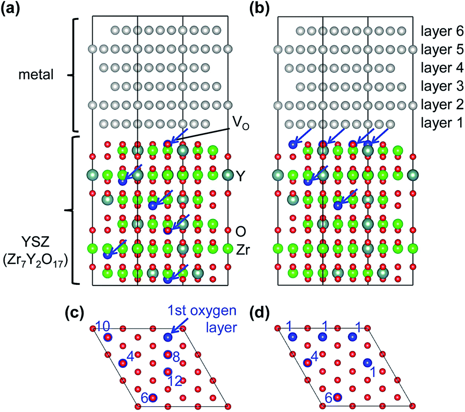 | ||
| Fig. 1 Structure models of planar incoherent (111) hetero-interfaces between metals (Pt or Au) and YSZ. (a) Non-segregated oxygen vacancy model, and (b) segregated oxygen vacancy model. Blue arrows mean oxygen vacancies. Numerical values in (c) and (d) represent the number of the oxygen layer counted from the interface in the middle in (a) and (b). | ||
3. Results and discussions
Fig. 2 shows plots of the total and projected electronic densities of states (DOS) corresponding to the spin-up state of segregated vacancy models for the two systems. The DOSs of spin-up and spin-down states were same in our models. The Fermi level is set at 0 eV. The Fermi level is located in the band gap of YSZ and consists of 6s and 6p orbitals of Au in the case of the Au/YSZ system. Small components of Au 5d orbitals also exist around the Fermi level. In contrast, large DOS of 5d orbitals of Pt traverses the Fermi level in the case of the Pt/YSZ system. In other words, the DOS near the Fermi level in the Au/YSZ system is less than that in the Pt/YSZ system.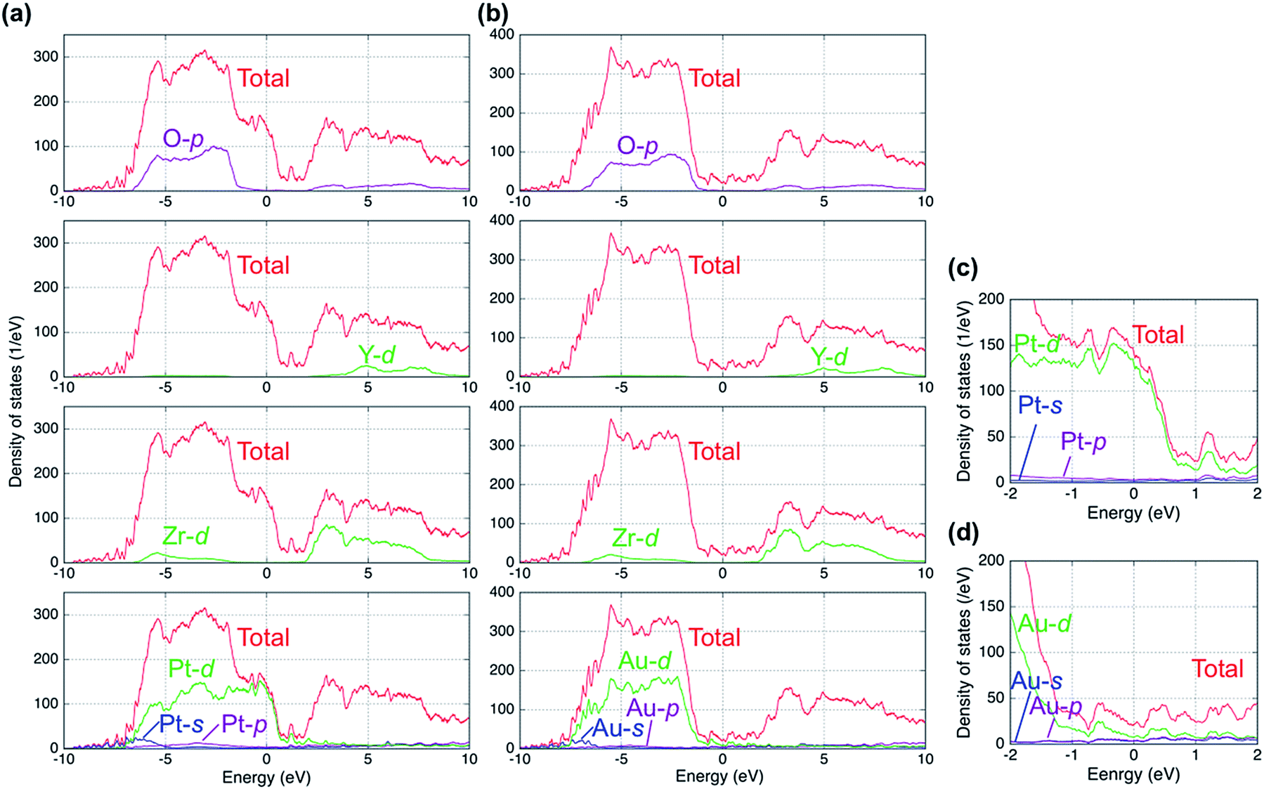 | ||
| Fig. 2 Calculated total and projected densities of states (DOS) for segregated vacancy models of (a) Pt(111)/YSZ(111) and (b) Au(111)/YSZ(111) interface systems. Magnified views of the projected DOS of (c) Pt and (d) Au near the Fermi level. | ||
Bader charge analysis was carried out to examine the distribution of charge within the metal slabs. Fig. 3 shows Bader charges of metal atoms as a function of position between interfaces in each model. In the bulk region of metal slabs (layers 2 to 5) Bader charges of metal atoms were similar for both the segregated vacancy model and the non-segregated vacancy model. In contrast, Bader charges of metal atoms in layers adjacent to the interfaces (layers 1 and 6) were very different, as their coordination/bonding environments are very different to those of atoms in the bulk. Specifically, in the segregated vacancy models, the Bader charges of metal atoms in layer 1 are much larger than those in layer 6. This is because oxygen vacancies in YSZ have effective positive charges, inducing more electrons to accumulate on atoms in the neighboring metal layer, layer 1. In contrast, the metal atoms in layer 6 lose more of their electrons on account of the larger population of negatively charged oxygen atoms in the neighboring layer to which they are bonded. Overall, charge neutrality is maintained.
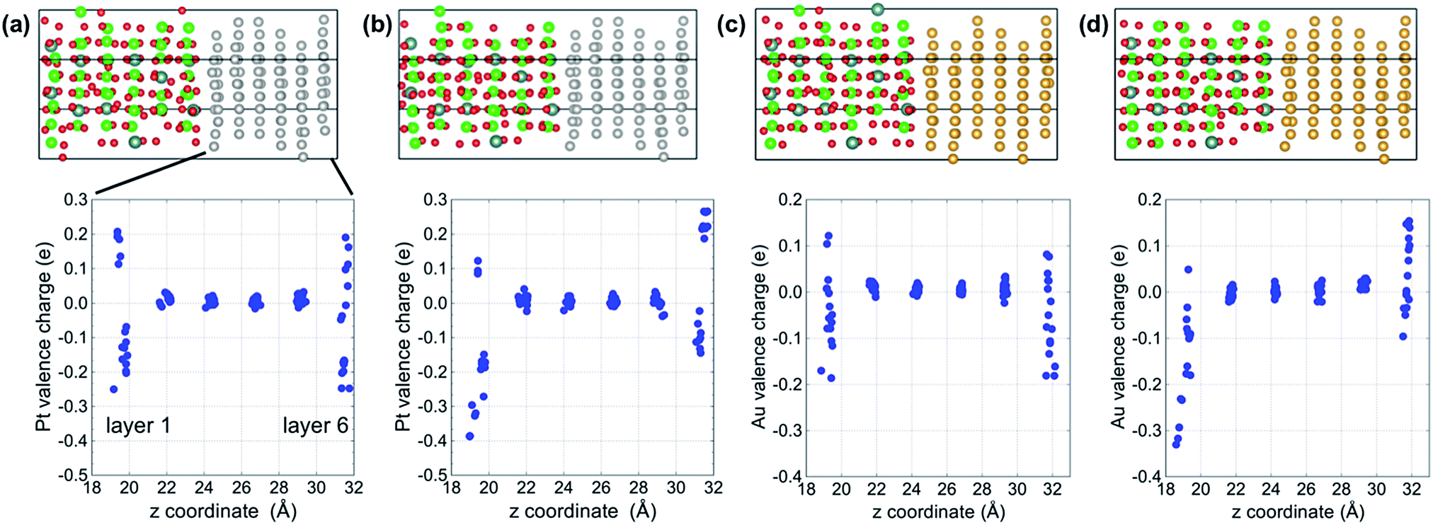 | ||
| Fig. 3 Bader charges of each metal atom as a function of position between interfaces. (a) Non-segregated vacancy model of Pt/YSZ, (b) segregated vacancy model of Pt/YSZ, (c) non-segregated vacancy model of Au/YSZ, and (d) segregated vacancy model of Au/YSZ. | ||
To examine the differences in electronic states between metal atoms in the segregated and non-segregated vacancy models in more detail, we calculated the average electron density of each metal layer normalized to the cross-sectional area. Fig. 4 shows the differences of the electron densities between metal atoms in the segregated and non-segregated vacancy models, Δρel = ρsegregatedel − ρnon-segel, where ρsegregatedel and ρnon-segel are the normalized average Bader charges of each layer in the segregated and non-segregated vacancy models, respectively. The values for layers 2 to 5 are almost zero. However, the metal layer adjacent to the vacancy-rich O layer in the segregated vacancy model (metal layer 1) is negatively charged (−0.31 C m−2 for Pt and −0.26 C m−2 for Au), while that adjacent to the fully occupied O layer (metal layer 6) is positively charged (0.33 C m−2 for Pt and 0.24 C m−2 for Au). These charges correspond to electron areal densities of 1.9 × 1014 cm−2, 1.6 × 1014 cm−2, 2.1 × 1014 cm−2 and 1.5 × 1014 cm−2, respectively. The changes in electronic charge on Pt and Au atoms in layers 1 and 6 are almost the same. This is mainly because oxygen concentrations in the YSZ layers adjacent to the metal slabs are the same for both models. Since the averages of Bader charges of oxygen atoms in each layer are almost the same for segregated and non-segregated vacancy models, the valence states of oxygen atoms do not affect the charge accumulation in the metal slabs. Such electronic charge accumulation in response to segregation of mobile ionic species is expected to result in an increase in the electronic conductivity of the metal layer, as reported for all-solid-state EDL transistors in (ref. 20). In addition, the metal slabs are simultaneously in contact with net positively- and net negatively-charged YSZ surfaces in the segregated vacancy hetero-interface model in this study. This periodicity of our hetero-interface models means that the change in Fermi level related on the catalytic properties in the vicinity of the biased metal-insulator interfaces cannot be determined quantitatively from our calculations. However, it is reasonable to assume that the effect of the bias on Fermi level of Au will be greater than that for Pt, because Au has lower DOS around the Fermi level than Pt (Fig. 2), i.e., the Fermi level shift induced by charge accumulation is larger in the case of Au/YSZ.
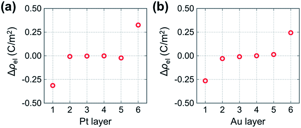 | ||
| Fig. 4 Difference in electron density between metal layers in the segregated and non-segregated vacancy models of (a) Pt/YSZ and (b) Au/YSZ. | ||
4. Summary
Planar interfaces between YSZ and metals Pt and Au have been computationally examined using first-principles calculations and Bader charge analysis within the framework of density functional theory. The DOS of the Au/YSZ interface around the Fermi level is lower than that of the Pt/YSZ interface on account of the lower density of Au 6s, 6p and 5d orbitals compared with the Pt 5d orbitals. Bader analysis revealed that the metal layers adjacent to the interface become positively or negatively charged when the bonding oxygen layer is rich or poor in oxygen vacancies, respectively. Metal atoms adjacent to an oxygen vacancy-rich interface were found to have higher electron densities than those adjacent to vacancy-free interfaces as a result of charge accumulation. The results indicate that segregation of oxygen vacancies to Au or Pt/YSZ hetero-interfaces alters the electronic conductivity of the layer of Au or Pt atoms adjacent to the interface relative to those in bulk metal.Acknowledgements
This work was partially supported by “Materials research by Information Integration” Initiative (MI2I) project of the Support Program for Starting Up Innovation Hub from Japan Science and Technology Agency (JST).Notes and references
- J. Maier, Nat. Mater., 2005, 4, 805–815 CrossRef CAS PubMed.
- J. Maier, J. Electroceram., 2015, 34, 69–73 CrossRef.
- K. Garrity, A. M. Kolpak, S. Ismail-Beigi and E. I. Altman, Adv. Mater., 2010, 22, 2969–2973 CrossRef CAS PubMed.
- H. L. Stadler, Phys. Rev. Lett., 1965, 14, 979–981 CrossRef CAS.
- C. Park and R. T. K. Baker, J. Phys. Chem. B, 2000, 104, 4418–4424 CrossRef CAS.
- C. Park and R. T. K. Baker, Chem. Mater., 2002, 14, 273–280 CrossRef CAS.
- N. Saito, Y. Yukawa and Y. Inoue, J. Phys. Chem. B, 2002, 106, 10174–10178 Search PubMed.
- A. M. Kolpak, I. Grinberg and A. M. Rappe, Phys. Rev. Lett., 2007, 98, 3–6 CrossRef PubMed.
- Y. Chiang, E. B. Lavik, I. Kosacki, H. L. Tuller and J. Y. Ying, Appl. Phys. Lett., 1996, 69, 185–187 CrossRef CAS.
- S. Kim and J. Maier, J. Electrochem. Soc., 2002, 149, J73–J83 CrossRef CAS.
- P. Lupetin, G. Gregori and J. Maier, Angew. Chem., Int. Ed., 2010, 49, 10123–10126 CrossRef CAS PubMed.
- I. Denk, J. Claus and J. Maier, J. Electrochem. Soc., 1997, 144, 3526–3536 CrossRef CAS.
- N. Sata, K. Eberman, K. Eberl and J. Maier, Nature, 2000, 408, 946–949 CrossRef CAS PubMed.
- B. Liu, V. R. Cooper, Y. Zhang and W. J. Weber, Acta Mater., 2015, 90, 394–399 CrossRef CAS.
- D. S. Aidhy, B. Liu, Y. Zhang and W. J. Weber, J. Phys. Chem. C, 2014, 118, 30139–30144 CAS.
- T. Tsuchiya, K. Terabe and M. Aono, Appl. Phys. Lett., 2013, 103, 3–7 CrossRef.
- K. Ueno, H. Shimotani, H. Yuan, J. Ye, M. Kawasaki and Y. Iwasa, J. Phys. Soc. Jpn., 2014, 83, 32001 CrossRef.
- H. Nakayama, J. Ye, T. Ohtani, Y. Fujikawa, K. Ando, Y. Iwasa and E. Saitoh, Appl. Phys. Express, 2012, 5, 23002 CrossRef.
- K. Taniguchi, T. Fukamichi, K. Itaka and H. Takagi, Adv. Funct. Mater., 2015, 25, 3043–3048 CrossRef CAS.
- T. Asano, Y. Kaneko, A. Omote, H. Adachi and E. Fujii, ACS Appl. Mater. Interfaces, 2017, 9, 5056–5061 CAS.
- G. Beck, H. Fischer, E. Mutoro, V. Srot, K. Petrikowski, E. Tchernychova, M. Wuttig, M. Rühle, B. Luerßen and J. Janek, Solid State Ionics, 2007, 178, 327–337 CrossRef CAS.
- P. E. Blöchl, Phys. Rev. B: Condens. Matter Mater. Phys., 1994, 50, 17953–17979 CrossRef.
- G. Kresse and D. Joubert, Phys. Rev. B: Condens. Matter Mater. Phys., 1999, 59, 1758–1775 CrossRef CAS.
- G. Kresse and J. Hafner, Phys. Rev. B: Condens. Matter Mater. Phys., 1993, 47, 558–561 CrossRef CAS.
- G. Kresse and J. Furthmüller, Phys. Rev. B: Condens. Matter Mater. Phys., 1996, 54, 11169–11186 CrossRef CAS.
- J. P. Perdew, K. Burke and M. Ernzerhof, Phys. Rev. Lett., 1996, 77, 3865–3868 CrossRef CAS PubMed.
- G. Henkelman, A. Arnaldsson and H. Jonsson, Comput. Mater. Sci., 2006, 36, 354–360 CrossRef.
- M. Yu and D. R. Trinkle, J. Chem. Phys., 2011, 134, 1–8 CrossRef PubMed.
- A. Zunger, S. Wei, L. Ferreira and J. Bernard, Phys. Rev. Lett., 1990, 65, 353–356 CrossRef CAS PubMed.
- M. Morinaga, J. B. Cohen and J. Faber Jnr, Acta Crystallogr., Sect. A: Cryst. Phys., Diffr., Theor. Gen. Crystallogr., 1979, 35, 789–795 CrossRef.
- P. Knauth and H. L. Tuller, J. Am. Ceram. Soc., 2004, 85, 1654–1680 CrossRef.
- K. Momma and F. Izumi, J. Appl. Crystallogr., 2008, 41, 653–658 CrossRef CAS.
- A. Predith, G. Ceder, C. Wolverton, K. Persson and T. Mueller, Phys. Rev. B: Condens. Matter Mater. Phys., 2008, 77, 144104 CrossRef.
| This journal is © The Royal Society of Chemistry 2017 |