
 Open Access Article
 This Open Access Article is licensed under a Creative Commons Attribution-Non Commercial 3.0 Unported Licence
Insight into metallic behavior in epitaxial half-metallic NiCo2O4 films
Kaiqi Zhanga,
Congmian Zhen *a,
Wengang Weiab,
Wenzhe Guoa,
Guide Tanga,
Li Maa,
Denglu Houa and
Xiancheng Wuc
*a,
Wengang Weiab,
Wenzhe Guoa,
Guide Tanga,
Li Maa,
Denglu Houa and
Xiancheng Wuc
aHebei Advanced Thin Films Laboratory, Department of Physics, Hebei Normal University, Shijiazhuang 050024, China. E-mail: cmzhen@hebtu.edu.cn
bState Key Laboratory of Surface Physics, Department of Physics, Fudan University, Shanghai 200433, China
cInstitute of Science and Technology for Opto-electronic Information, Yantai University, Shandong 264005, China
First published on 20th July 2017
Abstract
Understanding the cation distribution and electronic transport properties of half-metallic NiCo2O4 (NCO) films is crucial to advancing their practical applications in optoelectronic materials. In this work, the specific range of growth temperature (TG) and oxygen pressure (Op) for the metallic NCO film is obtained. The concentration of Ni3+ and NiTet ↔ CoOct exchange interactions are the primary determinants of metallic behavior in NCO thin films, which is demonstrated by the experimental and computational results. Theoretical simulation shows that the electron–electron and electron–magnon scattering intrinsically determined the metallic behavior. The growth temperature has a great influence on the structure and lattice constant of the NCO film. The film with metallic behavior has a relatively small lattice constant, which results in a large saturation magnetization. Due to the disordered cation in the metallic film, two magnetic phases were observed. The formation of the low-valence oxides at low Op and the cation vacancies at high Op make the NCO film have high resistivity.
Introduction
NCO is well known as an interesting mixed-valence transition metal oxide with an inverse spinel structure. Considering its advantages such as high electrochemical activity, low cost, rich abundance, and environmental friendliness, NCO has been extensively used in various fields, such as for supercapacitors,1,2 photo-detectors,3 and in various electrochemical reactions for O2 evolution.4 For these applications, understanding the microstructure and electrical conductivity behavior of NCO is very important. Previous studies mainly focused on amorphous or polycrystalline NCO nanostructures,5,6 which makes it difficult to characterize its intrinsic properties. Recently, some high-quality NCO nanostructures were reported. Hu et al. fabricated micrometer-sized NCO nanoplates, and electrical transport within an individual nanoplate is further investigated. The mechanisms of electrical conduction at low temperature (T < 100 K) can be explained in terms of Mott's variable range hopping model. At high temperature (T > 100 K), the electrical transport properties of the NCO nanoplate were contributed by the variable range hopping and the nearest neighbor hopping mechanism.7 Silwal et al. grew epitaxial NCO thin films on single crystalline MgAl2O4 (MAO) by pulsed laser deposition. Epitaxial NCO films grown at lower temperature (<450 °C) exhibit metallic behavior, while those grown at higher temperature are insulating.8 Bitla et al. have shown that NCO is ferrimagnetic metal, and the electric and magnetic behaviors are strongly correlated with the octahedral Ni3+. The metallic or semi-conductive properties of NCO can be tuned by the degree of cation site disorder via growth conditions.9 Growth temperature and O2 pressure are two key factors in controlling the conduction of NCO film. Up to now, few reports have discussed effects of both TG and Op on the conduction properties of the NCO film. Moreover, the electrical transport mechanism of NCO films still remains unclear.In this work, we obtained epitaxial NCO films on single crystal MAO substrate under different TG and Op. Metallic behavior is observed in the NCO film. The conductive mechanism of the NCO film has been investigated. The bonding structure and the cation distribution of the NCO thin films are analyzed in detail. The conductivity of the NCO film is closely associated with its magnetic properties.
Experimental and computation details
Epitaxial NCO thin films were fabricated on MAO (100) substrate by pulsed-laser deposition (PLD) with a laser energy density of 2.5 J cm−2 and repeat frequency of 10 Hz. Two series of the NCO films were prepared. The first series of the NCO films were grown at different TG from room temperature (RT) to 800 °C under a fixed Op of 50 mTorr. The second series of the NCO films were deposited under the Op range of 20–300 mTorr at a fixed TG of 350 °C.The structures of the films were investigated by high-resolution X-ray diffraction (HR-XRD, D8 Discover) and high-resolution transmission electron microscopy (HR-TEM, FEI Tecnai F20). The cross-sectional TEM samples were prepared by mechanical thinning and ion milling with 3.2–4.8 keV Ar+ ions for few hours. The surface morphologies of the NCO films were scanned using atomic force microscope (AFM, Nanoscope IV). The magnetic properties and temperature-dependence resistivity of the NCO films were measured by VSM and four-probe method in a physical property measurement system (PPMS). The bonding structure and chemical states of the films were characterized using Fourier transform infrared spectroscopy (FTIR) with a Nicolet 380 spectrometer. UV-visible absorption spectra were measured with a spectrophotometer (SHIMADZU, UV3600) at room temperature.
Electronic structure simulations based density functional theory were performed using CASTEP calculations on a spinel cubic cell containing 56 atoms in the reciprocal space. Lattice parameters were optimized by employing Perdew–Burke–Ernzerhof (PBE) functional within the generalized gradient approximation (GGA) with the additional Hubbard like term describing the onsite Coulomb interaction (U).10,11 Calculations were conducted with a Monkhorst–Pack grid of 4 × 4 × 4 k points.12 The electronic wave functions were expanded by using a plane wave basis set with an energy cutoff of 450 eV.
Results and discussion
NCO is believed to exhibit an inverse spinel structure with mixed-valence. In the crystallographic structure of NCO, Ni occupies the octahedral sites (Oct, B) and Co is distributed over both octahedral (Oct, B) and tetrahedral sites (Tet, A). The schematic of NCO inverse spinel is shown in Fig. 1a.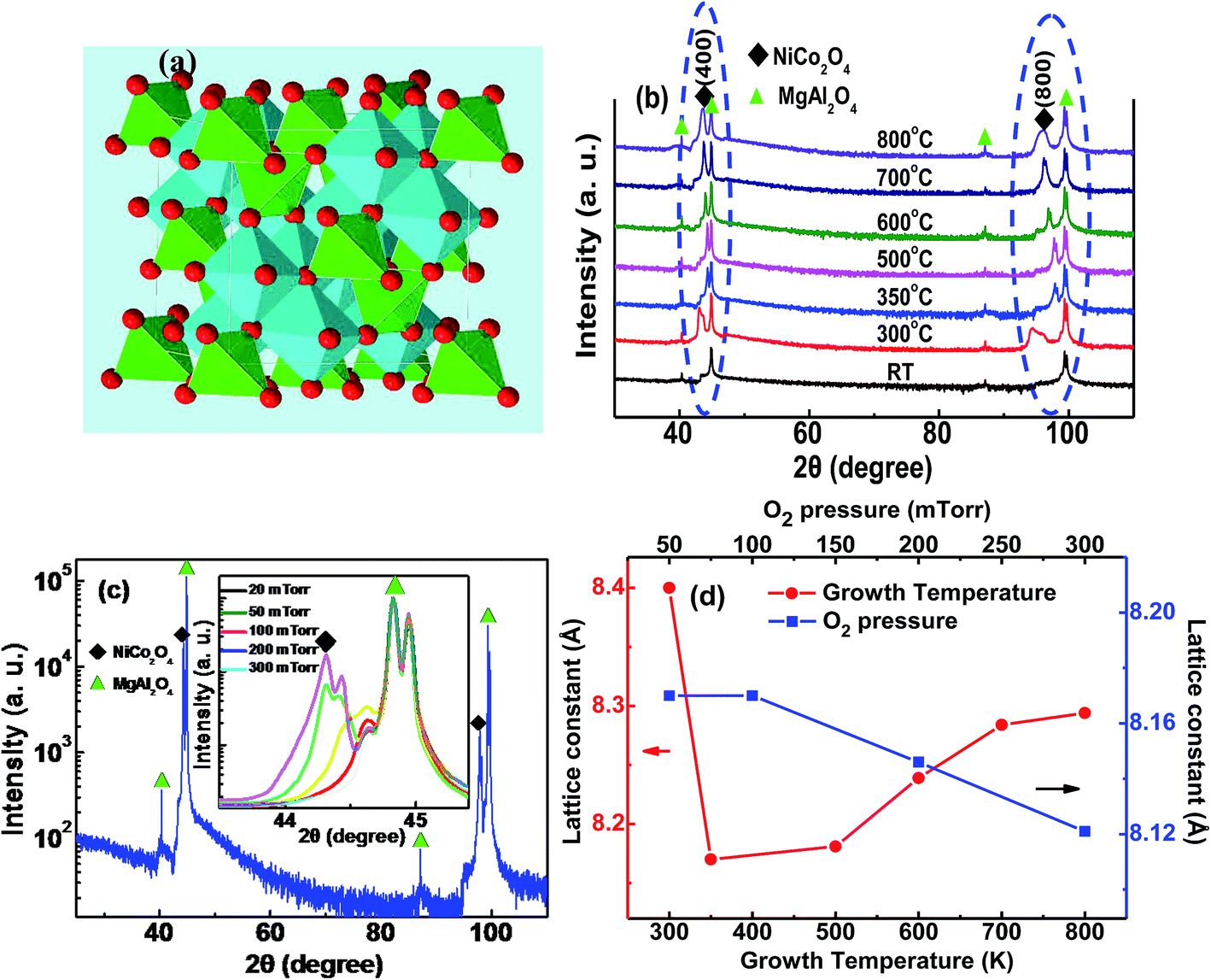 | ||
| Fig. 1 (a) Schematic of inverse spinel NiCo2O4, (b) XRD θ–2θ-scans of the NCO films grown under 50 mTorr Op at different TG, (c) XRD patterns of the NCO thin films grown under 50 mTorr Op at 350 °C, and (d) c-axis lattice parameter dependence on the Op/TG. The inset of (c) is the (400) peaks of the films prepared at different Op at 350 °C. | ||
The XRD measurements confirm that the NCO films are epitaxially grown on the MAO (100) substrate. The θ–2θ scan in Fig. 1b and c shows (400) and (800) reflection peaks of the inverse spinel NCO film and MAO substrate, without any identifiable peaks from secondary phases.
Fig. 1b shows the peaks of NCO thin films were grown at different TG under 50 mTorr Op. When the NCO film was grown at RT, no obvious peak was observed in the XRD pattern. When TG = 300 °C, diffraction peaks from the NCO film can be observed. However, the full widths at half maximum (FWHMs) of the peak of the film is larger. As the TG increased to 350 °C, the peaks of the NCO film moved toward higher angle with a decreased FWHMs. When we further raised the TG, the peaks shifted back to lower angle with an increased FWHMs. The smallest out-of-plane lattice constant (c) of 8.17 Å was obtained in the film grown at 350 °C via the peak location. The c value increased when the TG rised above 500 °C, shown in Fig. 1d. Such an interesting phenomenon that the growth temperature can control lattice constant of the film may be caused by not only the rate of cation-disorder but also their redistribution with mixed valence. We will discuss it in detail below.
We kept the TG unchanged at 350 °C. Fig. 1c presents the XRD patterns of the NCO thin films grown under 50 mTorr Op. In order to display the data more clearly, only the (400) peaks of the films prepared at different O2 pressure are shown in the inset of Fig. 1c. The splitting of the peaks was arisen by Cu Kα2 lines. Unlike the effect of TG, the c value decreased slightly with the increase of Op.
The reciprocal space mapping (RSM) scans around the (226) reflection of the NCO films with different growth conditions (Fig. 2a–c). The clear single NCO (226) peak directly below MAO (226) peak indicates the NCO has a high crystalline quality, while the same horizontal positions of NCO (226) and MAO (226) peaks imply that the films are fully compressively strained and have identical in-plane lattice constants (a) as the substrate. As we know, that the c value of bulk NCO is 8.114 Å. According to the vertical position, a larger c value of NCO films than substrate shows that the NCO suffered a compressive in-plane strain. This is consistent with the X-ray θ–2θ scan results.
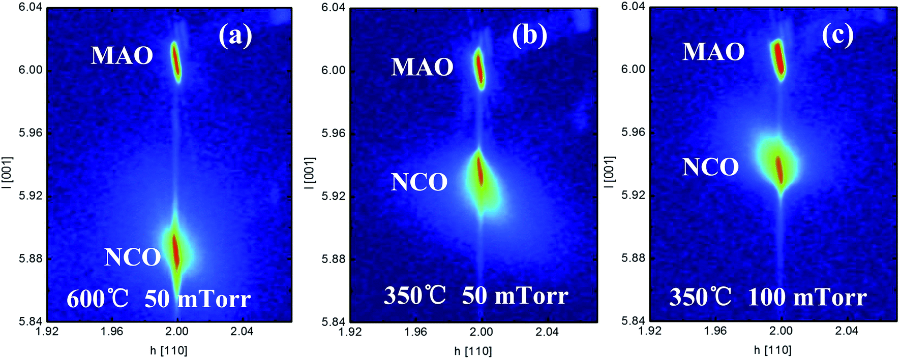 | ||
| Fig. 2 HR-XRD reciprocal space map around the (226) reflections of the NCO films on MAO substrate grown at (a) 600 °C, 50 mTorr Op, (b) 350 °C, 50 mTorr Op, and (c) 350 °C, 100 mTorr Op. | ||
To determine the crystal structure of NCO thin films precisely, the HR-TEM observations of the NCO film on MAO substrate (TG = 350 °C, Op = 50 mTorr) were conducted. Fig. 3a shows a cross-sectional HR-TEM image of the NCO film on MAO along the [100] direction. The arrows indicate the film/substrate interface. As can be seen, no misfit dislocations were observed at the interface and the atomic arrangements across the interface are coherent, indicating high quality and epitaxial growth of the films. In the HR-TEM image of the film, the dark diffused contrast of the structure is related to the tetrahedral cation vacancy.13 The selected area electron diffraction (SAED) patterns taken from the film and partial substrate show cubical arranged sharp with pure spots (Fig. 3b).
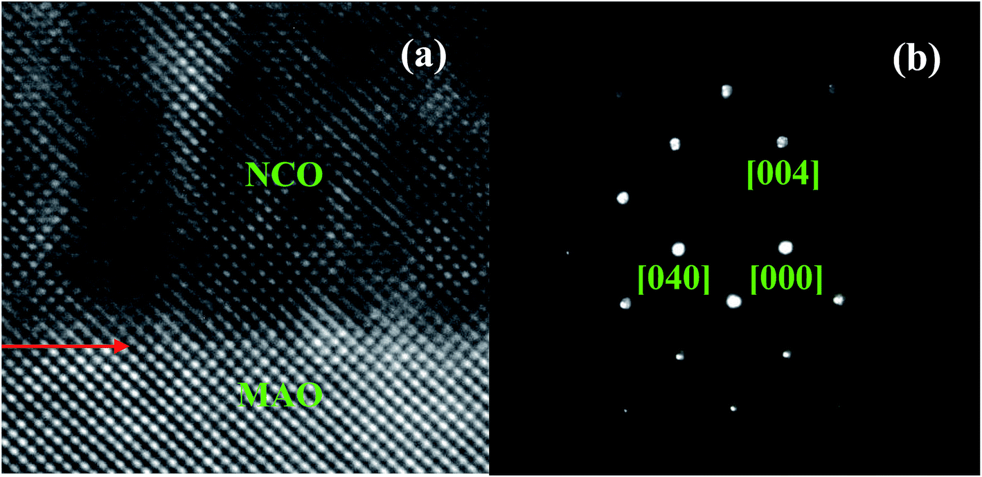 | ||
| Fig. 3 (a) Cross-sectional HR-TEM image of NCO/MAO and (b) selected area diffraction patterns along the [100] zone axis. | ||
The AFM (1 × 1 μm2) images in Fig. 4 show a fine scale scan of the NCO films' surface morphology. When the Op was 50 mTorr, the TG was at the range of 350–500 °C, the particle distribution is uniform and the average roughness (Ra) of the film is small. Lower or higher TG will make the film surface rough. The suitable growth temperature can provide certain energy for the deposited particles to move on the surface. At low TG, the particles deposited directly on the surface without enough energy to migrate to their proper location. High TG also let the particles accumulational, the surface will have a large roughness. Meanwhile, we can see that Op has a great influence on the surface morphology of the films. When the TG was 350 °C and the Op is 50 mTorr, the film had the smoothest surface (Fig. 4b). The agglomeration of NCO particles will occur (Fig. 4f) when the oxygen pressure is very high. We also note that lower Op makes the surface of the film uneven (Fig. 4f).
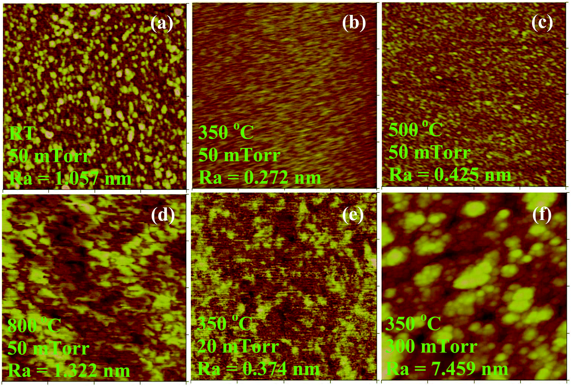 | ||
| Fig. 4 Surface morphologies of the NCO films grown under different TG and Op (1 × 1 μm2). | ||
According to the electricity measurements, TG and Op also play significant roles on the electrical transport of the NCO films. Compared with the previous report that the film shows metallic behavior when TG < 450 °C,14 our results indicate the films grown at 350–500 °C under 50 mTorr Op have metallic characteristics. The film grown at 350 °C exhibits the lowest resistivity of 0.34 mΩ cm at 82 K which is smaller than the reported lowest value of 0.8 mΩ cm.8 Films grown at TG < 350 °C or > 500 °C show semiconductor characteristics. The NCO film grown at 800 °C has the maximum resistivity (shown in Fig. 5a), and the resistance of the film is out of range of the ammeter at low temperature.
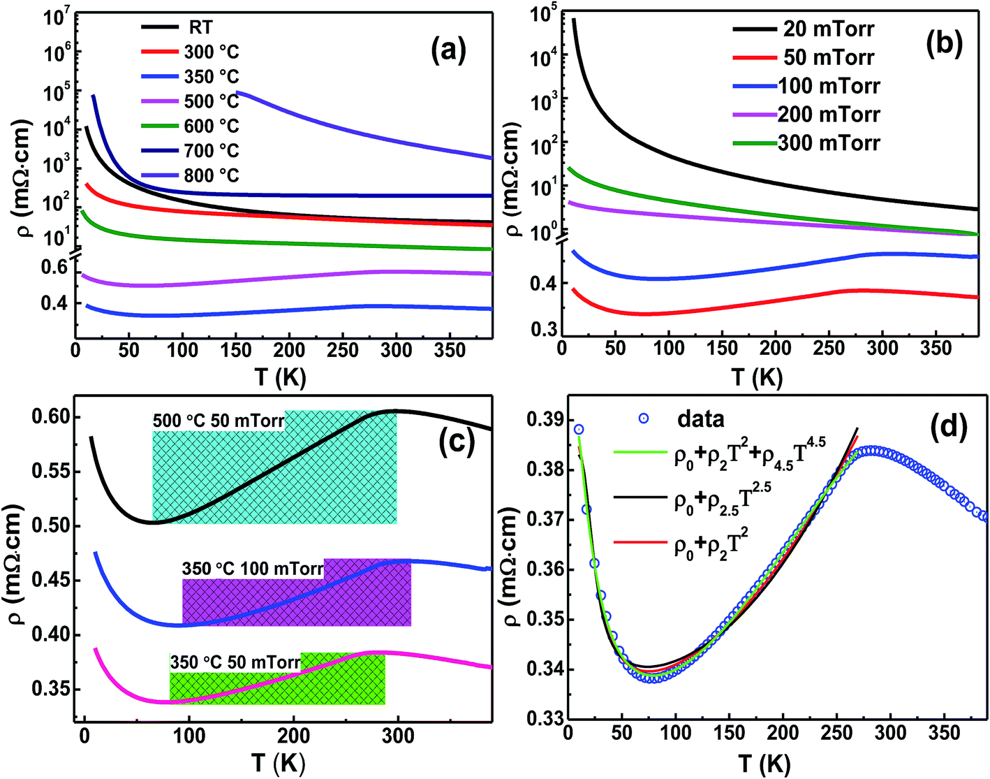 | ||
| Fig. 5 Resistivity vs. temperature for NCO films grown under (a) different TG at 50 mTorr Op, (b) different Op at 350 °C, (c) temperature window for metallic behavior in the NCO films marked with a rectangle, and (d) simulations on the semiconductor–metal transition of the film fabricated at TG = 350 °C and Op = 50 mTorr. | ||
The films grown at 50 and 100 mTorr Op with the TG = 350 °C show metallic behavior (Fig. 5a). However, when the Op is <50 mTorr or > 100 mTorr, the film shows semiconductor characteristics. Remarkably, lower O2 pressure makes the resistivity of the NCO film increase dramatically (Fig. 5b).
The temperature window for metallic behavior (TWm) in the NCO films has been marked in the Fig. 5c. When the Op = 50 mTorr and TG rises to 500 °C, the TWm became broadening with an increased resistivity interval. However, when the TG = 350 °C and Op increased to 100 mTorr, the TWm moved toward higher temperature. The active energy of charge carrier involved is determined by growth conditions. The further analysis about the change of TWm caused by TG and Op will be left to future work.
We simulated the semiconductor–metal transition of the metallic NCO film fabricated at TG = 350 °C and Op = 50 mTorr. The total resistivity of the NCO film is composed of the metallic part (ρm) and the semiconductive part (ρsc),15 which can also be confirmed by the later calculations on densities of states. For mixed valence NCO, the resistivity of metallic behavior (ρm) normally can be written as:
| ρm = ρ0 + ρ2T2 + ρ2.5T2.5 + ρ4.5T4.5 | (1) |
The temperature dependence of resistivity can be described for thermally activated conduction by
| ρsc = ρscdeEg/kBT + ρsc0 | (2) |
Then the total resistance (ρtot) of NCO thin film is described by
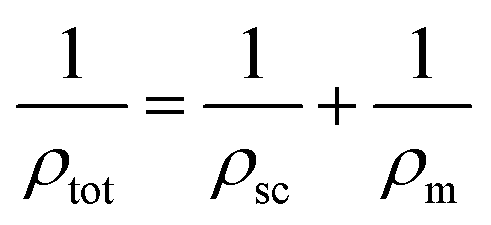 | (3) |
Here ρm presents three different mechanisms, then ρtot in eqn (3) will give three results. In contrast, only when the ρm is ρ2T2 + ρ4.5T4.5 goes quite well with the data in the whole temperature range (shown in Fig. 5d). It indicates that the e–e scattering and e–m scattering have significant contributions to the metallic behavior in the NCO film. The activation energy for the semiconductor part is 39.14 meV.
To further understand the conductivity of the film with metallic behavior, total and partial densities of states of the NCO structure were calculated, shown in Fig. 6. The results indicate that NCO is a half-metal material.20,21 The spin-up channel with a relatively small energy gap of ∼1.2 eV near the Fermi level. The gap of spin-up band is small enough so that the temperature can excite electrons to the conduction band. The densities of states of NiOct and CoTet crossed the Fermi level in the spin-down channel. The exchange interaction between NiOct and CoTet influences the conductivity of NCO.22
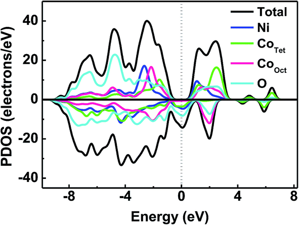 | ||
| Fig. 6 Calculations on the total and partial densities of states of the NCO. | ||
Infrared and Raman spectroscopy are used as effective tools for investigating the local structure of transition metal oxides. Iliev et al. gave a detailed analysis on Raman spectra of the NCO film.14 In this article, we studied the infrared spectroscopy of the films. There exist three infrared-active vibrational modes (Fig. 7). The higher frequency ν1 (680 cm−1) and ν2 (590 cm−1) modes involve primarily motion of the tetrahedral and octahedral Co–O, respectively.23–25 The lower frequency band ν3 corresponds to the vibrations of the octahedral Ni–O.24
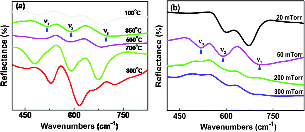 | ||
| Fig. 7 (a) Infrared spectra of the NCO films grown at different TG under 50 mTorr Op, and (b) different Op at 350 °C. | ||
As shown in Fig. 7a, the peaks of the metallic NCO films (TG = 350–500 °C) are weak and broad, indicting a mixed cation structure.25 Compared with the film with metallic behavior, the vibration modes of the film with semiconductor characteristics (TG < 350 °C or > 500 °C) shifted to lower wavenumber due to Ni3+ (radius, r = 0.056 Å) reduced to Ni2+ (r = 0.069 Å) with Ni–O bond length increasing. As the growth temperature increased, the vibration of bonds between metal cations and oxygen become violent. When the TG is 700 °C, the vibration peaks are symmetrical and sharp indicating that atomic arrangement in the NCO thin film has become more orderly. The structure of the semiconducting NCO film tends to be an ideal inverse spinel structure Co3+[Co3+Ni2+]O4.24,26 At high TG (800 °C), the vibration of the tetrahedron disappears and only two octahedral peaks exist, which shows that the spinel structure of NCO transforms to rock-salt structure.27
Fixed TG at 350 °C, O2 pressure also has great effects on the structure of the film. When the O2 pressure is low (20 mTorr), the bond number of (Ni–O)Oct decreased, which made the vibration intensity of ν3 weaken, shown in Fig. 7b. Low-valence transition metal oxide and oxygen vacancies were thought to be formed under low Op. Oxygen vacancy is generally thought to enhance the conductivity of the sample,28,29 but recent report shows that oxygen vacancy has only a minor effect electronic properties of the NCO film.22 Therefore, we think that low-valence oxide is mainly responsible for the high resistivity of the NCO film grown at 20 mTorr. Although the crystalline quality of the sample is poor at 20 mTorr, the bond of the lower valence metal ion with oxygen is observed in Fig. 7b. As the O2 pressure increase to 50 mTorr, more Ni3+ formed. The NCO film with mixed valence shows metal behavior with a low resistivity. No obvious peaks were observed at higher O2 pressure (≥200 mTorr). This is indicate that the NCO grown in oxygen-rich environment yields cation vacancies rather than incorporation of interstitial oxygen,30 which greatly affects the lattice vibration.
Differential UV-vis absorption spectrum is a useful method for determining electron transition energies between anions and cations.31,32 In this work, the occupations of the cations in the NCO thin films were investigated by differential UV absorption spectroscopy analysis (Fig. 8). Compared with the tetrahedral site, the octahedral site has lower energy. Based on the electronegativity difference between metal cations and oxygen, the octahedral cation transition energy in NCO is determined. The relation of different cation electronegativities is as follow: Co2+ (1.321) < Ni2+ (1.367) < Co3+ (1.693) < Ni3+ (1.695).33 Oxygen electronegativity is higher than those of cations. Therefore, the Ni3+ located at the lowest energy. The intensity of the NiOct3+ peak at 1.85 eV is relatively strong for the metallic NCO films (Fig. 8a and b). Therefore, the Ni3+ was thought to be decisive for metallic behavior in NCO thin films. When a Ni2+ is converted to Ni3+ at octahedral site, the bond length of (Ni–O)Oct decreased by 0.013 Å. Considering that electron transfer takes place from Ni eg level to Co t2g level, Co3+ (0.061 Å) changed into Co2+ (0.075 Å). There are two cases to consider: one is that there is no enough thermal energy to make the tetrahedra expand, the enlarged Co2+ ions can't enter into the tetrahedral site, and cation vacancies will form. Tetrahedral cation vacancies (TCV) in NCO film were often observed in other reports.26 The formation of TCV results in the decrease in the lattice constant of the NCO film. The other case is that the volume of the tetrahedra is large enough to accommodate Co2+ with the bond length of (Co–O)Tet increasing by 0.014 Å. One can note that the (Ni–O)Oct bond is parallel to the 〈100〉 direction, while the (Co–O)Tet bond has a certain angle with the 〈100〉 direction. So the bond length of (Co–O)Tet increases along the 〈100〉 direction by 0.006 Å. The changes of the (Ni–O)Oct and (Co–O)Tet bonds in the metallic films eventually lead to the decrease of the lattice constants. While, in the semiconducting film, Ni mainly existed as Ni2+ (2.04 eV) at octahedral site (Fig. 8a and b). The peak of the octahedral Co3+ located at 1.99 eV was detected in both the metallic and insulating films. As the TG was rised up to 800 °C, it is mainly composed of octahedral Ni2+ and Co2+ (2.04 eV) and the peak of the tetrahedral Co (2.36 eV) gradually disappeared (Fig. 8a).
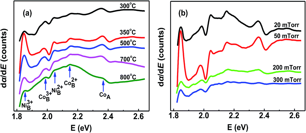 | ||
| Fig. 8 Curves of the differential absorption coefficient vs. photon energy for the NCO films grown (a) at different TG with 50 mTorr Op, and (b) different Op at 350 °C. | ||
Fig. 9a and c show the temperature dependent (T) magnetization (M) under 1 kOe magnetic field. For the metallic films, we also gave the zero-field cooling (ZFC) measurement results under a 1 kOe magnetic field. We can see that the film with metallic behavior has a large M. More importantly, two transition temperatures are observed for the metallic film. The higher transition temperature corresponds to the Neel temperature, which can be seen in the resistance measurements. We confirm that there exists two magnetic phases in the film with metallic behavior and the two phase has different Curie temperature. The two phases are mainly caused by the cation disorder. While, there is only one low transition temperature in the semiconductor films, thought to be the Neel temperature. Fig. 9b and d display the M–H hysteresis curves of these films measured at 5 K. The film with metallic behavior has a large MS, and a relatively small coercivity (HC). The conductivity of the film mainly depend on the A–B double-exchange and the ferromagnetism was mainly decided by the A–B double-exchange and B–B super-exchange couplings (due to the long distance between A–A, the interaction between A–A can be neglected).22 The metallic film has relatively small lattice constant, which enhance the interaction of A–A and A–B and result in large MS and small HC.34 However, high O2 pressure result in many cation vacancies, which made the film grown at 200 mTorr have a large MS (Fig. 9c and d).
 | ||
| Fig. 9 M–T and FC-ZFC curves of the NCO films grown at different: (a) TG, and (c) Op. Hysteresis loops of the NCO films grown at different: (b) TG, and (d) Op. | ||
Conclusions
Epitaxial NCO thin films were grown on MAO (100) substrate by PLD with different TG and Op. Under a special range of Op (50–100 mTorr) and TG (350–500 °C), the film has shown metallic characteristics with the lowest resistivity being 0.34 mΩ cm. The low-valence oxides formed at low Op and cation vacancies formed at high Op lead to high resistivity of the NCO film. The growth temperature makes the structure and lattice constant of the film change significantly. The films with metallic properties have small lattice constant and smooth surface. The interactions between NiOct and CoTet as well as high concentration of Ni3+ are thought mainly contributed to the metallic behavior in the NCO films. Theoretical study indicates that NCO is a half-metal material and the conductive mechanism of the metallic behavior is e–e scattering and e–m scattering. Two magnetic phases caused by cation disorder in the metallic film was observed. The film with metallic behavior has a large saturation magnetization. The metallic behavior in NCO film could be tuned by growth temperature and O2 pressure.Acknowledgements
We would thank Professor Jian Shen (Fudan University) for fruitful discussions. This work was partly supported by the National Natural Science Foundation of China (Grant No. 10804026 and 11504247), the Key Project of Natural Science of Hebei Higher Education under Grant No ZD2017045, and Hebei talent engineering (A201400119).Notes and references
- G. Q. Zhang and X. W. Lou, Adv. Mater., 2013, 25, 976–979 CrossRef CAS PubMed.
- G. Q. Zhang, H. B. Wu, H. E. Hoster, M. B. Chan-Park and X. W. Lou, Energy Environ. Sci., 2012, 5, 9453–9456 CAS.
- L. F. Hu, L. M. Wu, M. Y. Liao and X. S. Fang, Adv. Mater., 2011, 23, 1988–1992 CrossRef CAS PubMed.
- B. Cui, H. Lin, J. B. Li, X. Li, J. Yang and J. Tao, Adv. Funct. Mater., 2008, 18, 1440–1447 CrossRef CAS.
- J. G. Kim, D. L. Pugmire, D. Battaglia and M. A. Langell, Appl. Surf. Sci., 2000, 165, 70–84 CrossRef CAS.
- R. Alcántara, M. Jaraba, P. Lavela and J. L. Tirado, Chem. Mater., 2002, 14, 2847–2848 CrossRef.
- L. F. Hu, L. M. Wu, M. Y. Liao, X. H. Hu and X. S. Fang, Adv. Funct. Mater., 2012, 22, 998–1004 CrossRef CAS.
- P. Silwal, L. D. Miao, I. Stern, X. L. Zhou, J. Hu and D. H. Kim, Appl. Phys. Lett., 2012, 100, 032102 CrossRef.
- Y. Bitla, Y. Y. Chin, J. C. Lin, C. Van Nguyen, R. Liu, Y. Zhu, H. J. Liu, Q. Zhan, H. J. Lin, C. T. Chen and Y. H. Q. He, Sci. Rep., 2015, 5, 15201 CrossRef CAS PubMed.
- J. P. Perdew, K. Burke and M. Ernzerhof, Phys. Rev. Lett., 1996, 77, 3865–3868 CrossRef CAS PubMed.
- S. L. Dudarev, G. A. Botton, S. Y. Savrasov, C. J. Humphreys and A. P. Sutton, Phys. Rev. B: Condens. Matter Mater. Phys., 1998, 57, 1505–1509 CrossRef CAS.
- H. J. Monkhorst and J. D. Pack, Phys. Rev. B: Solid State, 1976, 13, 5188–5192 CrossRef.
- R. Datta, B. Loukya, N. Li and A. Gupta, J. Cryst. Growth, 2012, 345, 44–50 CrossRef CAS.
- M. N. Iliev, P. Silwal, B. Loukya, R. Datta, D. H. Kim, N. D. Todorov, N. Pachauri and A. Gupta, J. Appl. Phys., 2013, 114, 033514 CrossRef.
- M. Saloaro, S. Majumdar, H. Huhtinen and P. Paturi, J. Phys.: Condens. Matter, 2012, 24, 366003 CrossRef CAS PubMed.
- J. M. D. Teresa, M. R. Ibarra, J. Blasco, J. Garcia, C. Marquina, P. A. Algabel, Z. Arnold, K. Kamenev, C. Ritter and R. von Helmolt, Phys. Rev. B: Condens. Matter Mater. Phys., 1996, 54, 1187–1193 CrossRef.
- G. J. Snyder, R. Hiskes, S. DiCarolis, M. R. Beasley and T. H. Geballe, Phys. Rev. B: Condens. Matter Mater. Phys., 1996, 53, 14434–14444 CrossRef.
- A. Urushibara, Y. Moritomo, T. Arima, A. Asamitsu, G. Kido and Y. Tokura, Phys. Rev. B: Condens. Matter Mater. Phys., 1995, 51, 14103–14109 CrossRef CAS.
- L. Pi, L. Zheng and Y. H. Zhang, Phys. Rev. B: Condens. Matter Mater. Phys., 2000, 61, 8917–8921 CrossRef CAS.
- P. F. Ndione, Y. Z. Shi, V. Stevanovic, S. Lany, A. Zakutayev, P. A. Parilla, J. D. Perkins, J. J. Berry, D. S. Ginley and M. F. Toney, Adv. Funct. Mater., 2014, 24, 610–618 CrossRef CAS.
- P. Li, C. Xia, D. X. Zheng, P. Wang, C. Jin and H. L. Bai, Phys. Status Solidi RRL, 2016, 2, 190–196 CrossRef.
- X. Shi, S. L. Bernasek and A. Selloni, J. Phys. Chem. C, 2016, 120, 14892–14898 CAS.
- Y. E. Roginskaya, O. V. Morozova, E. N. Lubnin, Y. E. Ulitina, G. V. Lopukhova and S. Trasatti, Langmuir, 1997, 13, 4621–4627 CrossRef CAS.
- P. Nkeng, G. Poillerat, J. F. Koenig, P. Chartier, B. Lefez, J. Lopitaux and M. Lenglet, J. Electrochem. Soc., 1995, 142, 1777–1783 CrossRef CAS.
- M. E. Donders, H. C. M. Knoops, M. C. M. van de Sanden, W. M. M. Kessels and P. H. L. Notten, J. Electrochem. Soc., 2011, 159, G92–G96 CrossRef.
- K. Dileep, B. Loukya, P. Silwal, A. Gupta and R. Datta, J. Phys. D: Appl. Phys., 2014, 47, 405001 CrossRef.
- S. Y. Tsai, K. Z. Fung, C. N. We and H. Y. Bor, J. Electron. Mater., 2014, 43, 2584–2587 CrossRef CAS.
- Y. C. Wang, T. Zhou, K. Jiang, P. M. Da, Z. Peng, J. Tang, B. Kong, W. B. Cai, Z. Q. Yang and G. F. Zheng, Adv. Energy Mater., 2014, 1400696 CrossRef.
- J. Bao, X. D. Zhang, B. Fan, J. J. Zhang, M. Zhou, W. L. Yang, X. Hu, H. Wang, B. C. Pan and Y. Xie, Angew. Chem., 2015, 127, 7507–7512 CrossRef.
- G. Subias, J. Garcia, J. Blasco and M. G. Proietti, Phys. Rev. B: Condens. Matter Mater. Phys., 1998, 58, 9287–9293 CrossRef CAS.
- J. Melsheimer, S. S. Mahmoud, G. Mestl and R. Schlögl, Catal. Lett., 1999, 60, 103–111 CrossRef CAS.
- L. C. Xue, L. Q. Wu, S. Q. Li, Z. Z. Li, G. D. Tang, W. H. Qi, X. S. Ge and L. L. Ding, Phys. B, 2016, 492, 61–64 CrossRef CAS.
- K. Y. Li and D. F. Xue, J. Phys. Chem. A, 2006, 110, 11332 CrossRef CAS PubMed.
- H. S. Kim and H. M. Christen, J. Phys.: Condens. Matter, 2010, 22, 146007 CrossRef CAS PubMed.
| This journal is © The Royal Society of Chemistry 2017 |