
 Open Access Article
 This Open Access Article is licensed under a
 Creative Commons Attribution 3.0 Unported Licence
Coupling effects of strain on structural transformation and bandgap engineering in SnS monolayer
Yu Zhang,
Bo Shang *,
Lingjie Li and
Jinglei Lei
*,
Lingjie Li and
Jinglei Lei
College of Chemistry and Chemical Engineering, Chongqing University, Chongqing 400044, PR China. E-mail: bshang@cqu.edu.cn
First published on 12th June 2017
Abstract
The anisotropy strain effects on black phosphorus and the IV–VI monolayer analogues have been widely investigated due to their potential applications in solar energy conversion and opto-electronics. Although the coupling effects of strain on structural and electronic properties might be important in flexible monolayer materials they were neglected in most cases. In this paper, we investigated the strain effect on the properties of SnS via strain induced potential energy surface and band profiles. Our first-principles calculations predict different types of low-dimensional phases under ununiformed biaxial strain of 19.09 N m−1, with either strain induced semiconductor–metal transitions, indirect–direct bandgap transitions or negative Poisson's ratio. Our calculations suggest a new method to illuminate the strain effect beyond the axis direction, demonstrating that the coupling of strain effect plays an important role in the search for new properties for flexible materials and cannot be neglected.
1. Introduction
Nowadays, the black phosphorus (BP)1 and IV–VI2–6 monolayer have attracted considerable attention due to their unique puckered structure and potential applications in fields such as solar energy conversion7–9 and opto-electronics.10–12 The electronic and optical performances are essentially decided by atomic structures.13 As a flexible monolayer, the strain is the most direct and effective way to change the atomic and electronic structures.14,15 The anisotropic strain mechanisms for properties controlling of BP, GeX and SnX (X = S, Se, Te) have been widely investigated and their strain induced bandgap engineering has been confirmed.16–19 All types of strain on structural and electronic properties are important for strain effect investigation, which has been proved in the strain engineering of graphene.20 Till now, most of the anisotropic strain was applied in the zigzag and armchair direction and only the uniaxial strain and unique biaxial strain have been considered.16–19,21,22 The coupling of the strain effects are mostly neglected, which might play an important role in bandgap and optical modulations.Recently, one of the phosphorus-like monolayer SnS was successfully fabricated with liquid-phase exfoliation method.23 The monolayer SnS is a typically IV–VI non-toxic semiconductor, with an indirect band gap similar to silicon with a large absorbance coefficient (α > 104) across the ultraviolet, visible and near infrared regions of the electromagnetic spectrum. Since both elements are quite abundant in the earth, it is a promising material for flexible photovoltaic applications.24–27 The SnS monolayer shares similar layer structure with black phosphorus, with the exception that two kinds of atoms occupy the positions of phosphorus atoms in black phosphorus, which breakdown the symmetry.28–30 Unlikely the widely investigated phosphorus, a comprehensive study of strain on the structural stability, electronic and optical properties of monolayer SnS has not carried out yet. The mechanical properties of monolayer SnS still need further investigation.31–35
In this paper, we investigate the structural, electronic and optical properties of monolayer SnS based on strain-induced-potential energy surface (SIPES) and band profiles (SIBP) within the density functional theory (DFT). The SIPES can be used to investigate not only the axial strain but also the coupling effect due to the anisotropic strain. We systematically investigate the relationship between the strain induced structure and properties for monolayer SnS. We suggest several types of monolayer models with different symmetry group in response to a pressure less than 19.09 N m−1. A negative poisson's ratio have been predicted in monolayer SnS with axis strain less than 2%. Furthermore, the modulation of electronic properties for monolayer SnS can be described with a strain-based band profile effectively, resulting a semiconductor to metal transition and indirect–direct–indirect band gap transition. Our results indicate via strain-engineered, and used as a photovoltaic material.
2. Computational methods
First-principles calculations within the density functional theory (DFT) methods were carried out in the Vienna ab initio simulation package (VASP).36–38 The PBE methods have been employed to investigate the structural stability and electronic properties, and the HSE hybrid functional methods have been used to check the band gaps of all the cases employed here to overcome the problem of band gap underestimation in PBE functional.39,40 The projector augmented wave (PAW) method is used to describe the electron–ion interaction, and the valence electrons of 4s24p2 for Sn and 3s23p4 for S atoms have been adopted in the calculations.33,41 A energy cutoff of 450 eV and appropriate Monkhorst–Pack K meshes grid under structure relax and the more precise K mesh with 15 × 15 × 1 are adopted in electrons calculations. A vacuum slab larger than 15 Å is used to eliminating interaction between adjacent images.42 All the structures are fully relaxed with a force tolerance of 0.01 eV Å−1 and the convergence criterion on the total energy is 10−6 eV.43 We checked the possible spin effects, which hardly change the band structures. The optical absorption spectra calculation is within the transversal approximation at the DFT/PBE level.3. Results and discussion
The relaxed monolayer SnS have three Sn and three S atoms in each conventional unit cell with the space group Pmn21 as shown in Fig. 1.44 We obtained the monolayer SnS with the cell parameters (a = 4.05 Å, b = 4.34 Å) (PBE), in accordance to the experimental results31 (a = 3.99 Å, b = 4.34 Å) and the result of other authors16,45 are shown in Table 1 altogether. The detailed structures are plotted in Fig. 1. The indirect gap in our band calculation is 2.09 eV (HSE06), which is in good agreement with 2.03 eV reported in other theoretical works.16 These results indicate that our calculation methods are highly reliable.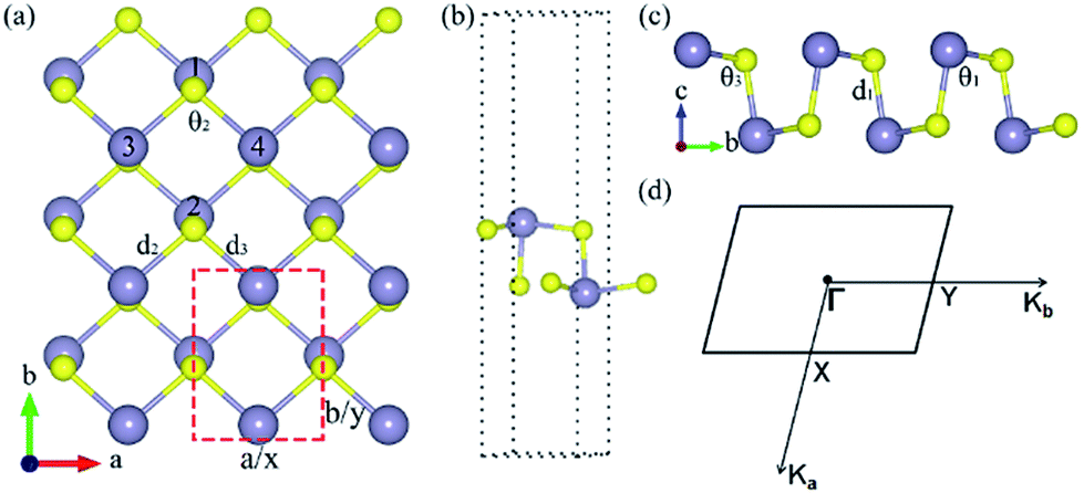 | ||
| Fig. 1 The lattice structure of monolayer SnS from (a) top and (c) side view. (b) The unit cell of monolayer SnS. (d) Brillouin zone with high-symmetry points labeled. The d1 is the out-of-plane bond length and d2, d3 are the in-plane bond lengths, respectively, and θ2 is the in-plane bond angle and θ1, θ3 are the out-of-plane bond angles, respectively. The atoms plotted in purple and yellow are Sn atoms and S atoms, respectively. | ||
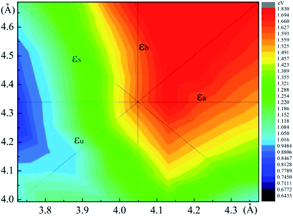
The SIPES with corresponding external pressures are plotted in Fig. 2(a) and (b). The x-axis and y-axis represent the change of cell parameter a and b respectively. The a/b vectors respect to the armchair/zigzag direction respectively in BP-liked material.16,45 The strains and deformation (εx, εy) can be calculated from the deformed cell parameters with the formula (a/astrainless − 1, b/bstrainless − 1). With the unique puckered structure, strain limit for SnS might be bigger than that of graphene (∼15%).46 In our calculations, the deformation ranged from −20% to 20% on each axis and −10% to 10% on the grid mesh are considered at a uniform size of 2%. As shown in Fig. 2(a), the most stable area is the bottom of energy valley, which followed the direction of strain εs. The stable valley in SIPES means that while pushing the layer in one direction, the layer should extend in another direction to release the stress, corresponding to the experimental condition under uniaxial strain with internal stress released. The external pressures were plotted Fig. 2(b).
 | ||
| Fig. 2 (a) and (b) are the energy and external pressure of system versus applied biaxial strain for monolayer SnS. | ||
The variations of bond lengths and angles under uniaxial strain have been plotted in Fig. 3(a) and (b). With the deformation changed from −14% to 18% on x-axis direction, the bond length d1 decreased from 2.60 to 2.55 Å, which means that the pull or push strength effect on the height of layer is not significant: with deformation of 2% on y-axis, the height of monolayer enhanced about 4%. This enhancement means that monolayer SnS have a negative poisson's ratio similar with black phosphorus.47 The horizon bond lengths (d2 and d3) will change from 2.60 Å to about 2.88 Å with the angles of S–Sn–S (θ2) in the horizon increase from 85° to 115°. The other types of S–Sn–S angles (θ1 and θ3) will decrease, and the coordinate numbers of the surface atoms will change from three to five gradually. In general, monolayer SnS tends to stabilize through keeping the layer thickness (d1), changing the in-plane angle (θ2) and forming a flat parallelogram along a or b direction. Even under the strain (−20%, 20%), the Sn and S atoms are still at same height, as shown in Fig. 4(b).
 | ||
| Fig. 3 Calculated structural parameters ((a) S–Sn bond lengths d1, d2, d3; (b) bond angles θ1, θ2, θ3) applied biaxial strain for monolayer SnS. The positive and negative strains mean the stretched and compressed lattice constants, respectively. | ||
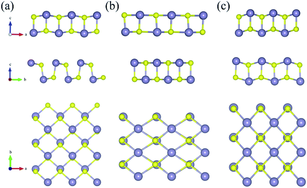 | ||
| Fig. 4 Top view and side view of three typically SnS monolayer models. The space group for (a–c) is Pmn21, Pm and Pmmn respectively, which is corresponding to the strain (0%, 0%), (20%, −20%) and (−8%, −6%). | ||
The most unstable regions in Fig. 2(a) and (b) are located in the lower left with bright yellow colors. In these areas, structures experience a large pressure. Generally, monochalcogenides of group-IV elements are isoelectronic with phosphorus, and their structures are reminiscent of corrugated phosphorene. However, because of the two atomic species and two-dimensional character, the symmetry of monolayer SnS loses inversion symmetry, with a Pmn21 space group.30,44,48 In this structure, the Sn2+ ion coordinates to three S2− ions, with the Sn 5s2 lone pair occupying the last position of a tetrahedral geometry, forming a revised lone pair model. Under biaxial compressed strain εu, the pressure is not easily to release compared with uniaxial, thus the Sn and S atoms are not on the same height, which makes the height of layer much bigger as shown in Fig. 4(c). And the space group will change from Pmn21 to Pmmn with the enhancement of biaxial pressures44,49
In order to detect strain-induced modulation of electronic properties, we plotted the band gap profile as shown in Fig. 5. Four types of strain are concerned, including two types of uniaxial strain εa, εb and two types of biaxial strain εu and εs. It demonstrates that applying strain is an efficient approach to modulate the electronic properties, especially the size of band gap. With a strain ranging from −10% to 10%, the band gap exhibits a linear increase along εb, while it increases with the absolute value of εa. The band gaps continuously drop while applying biaxial compressive strain εu, and the biaxial stretched strain produces the contrary effect. Particularly, we focus on the bandgap engineering with uniaxial strain εs, which is energy favorable under uniaxial strain. The bandgap varies from 1.1 eV to 1.58 eV while the strain changed from (−14%, 14%) to (0%, 0%), as shown in Fig. 6(a). However, the bandgap tempestuously changes from 1.58 eV to 1.60 eV under the (2%, −2%) strain, and then drop sharply, even below 0 eV under the strain (16%, −16%). The result indicates that the pressure followed the εs direction will easily perform while modulating the band gap of monolayer SnS, which is also shown in Fig. 5(a).
 | ||
| Fig. 5 Evolution of band gaps of SnS monolayer as a function of various biaxial strains. | ||
 | ||
| Fig. 6 (a) Evaluation of the effect of the biaxial strain εs on the band gaps of monolayer SnS. (b–d) are energy band structures and PDOS of monolayer SnS without strain and with strain (−14%, 14%) and (16%, –16%). | ||
To get more details about the bandgap modulation mechanism, we draw the band structures and partial density of states (PDOS) for the models with (−14%, 14%), no strain and (16%, −16%), as shown in Fig. 6(b)–(d), respectively. Without strain (see Fig. 6(b)), the monolayer SnS is an indirect band gap semiconductor with a gap of 1.58 eV. With the application of the biaxial strain εs, the conductive band (CB) will change dramatically, especially on the points of Γ, Γ–X, Γ–Y. While pulling in b direction up to 14%, Sn-1 is gradually far away from the Sn-2. As a result, the conductive band minimum (CBM) gradually shrinks at Γ–Y (see Fig. 6(c)). At the same time, with the strain up to −14% along a direction, the Sn-3 is closer to Sn-4, therefore CB gradually moves down, which can be ascribed to the increases of bandwidth at Γ–X. However, the cell parameter b is larger than a, thus the CBM at Γ–X moves slowly. In turn, with the strain (−16%, 16%), the CB at Γ–Y moves down rapidly and the CBM even below the Fermi energy at the Γ–Y sites, which make the monolayer SnS change from semiconductor to metal. The external stress of model is about 1.31 N m−1 from Fig. 2(b), which might be easily achievable in experiment. The PDOS of monolayer SnS for selected cases also indicates that the CBM at Γ–Y is mainly composed by Py and Pz orbitals of Sn atom, giving rise to the metal properties of monolayer SnS.
From above, we found that the CBM is sensitive to strain. To get a better understanding of the strain coupling effect on band profile, we explore strain effect on energy and sites of CBM and valence band maximum (VBM), as shown in Fig. 7(a–d), thus the effect of VBM sites could be neglected in Fig. 7(b). As shown in Fig. 7(a) and (b), the energy change of the VBM under strain is few, and thus the changes of the CBM map is similar to the bandgap shown in Fig. 5. Besides, we know that not only the band gap but also the sites of VBM and CBM can affect the optical properties. Here, strain induced sites of the CBM and VBM are plotted in Fig. 7(c) and (d). By comparison, we found that for most of areas, the band types are indirect except the areas around (−8%, 0%). The no-strain SnS exhibits indirect gap with a conduction band minimum (CBM) locating at the Γ–Y point and the valence band maximum (VBM) locating at the X–Γ point. With strain (−8%, 0%), the green location of the valence band maximum (VBM) and the conduction band minimum (CBM) (see Fig. 7(c)) overlap each other and eventually touch at Γ point, forming a direct gap of 1.50 eV under appropriate strain.
 | ||
| Fig. 7 (a) Energy and (c) location of the three states including ΓCBM, Γ–XCBM, Γ–YCBM and (b) energy and (d) location of the three states including ΓVBM, Γ–XVBM, Γ–YVBM for monolayer SnS as functions of deformed cell vector a and b. | ||
To facilitate a closer inspection of the special cases, we display the detailed band structures of (0, −7%), (0, −8%) and (0, −9%) in Fig. 8. When the strain is 7% (black line), the VBM locates at Γ–Y. As the strain increases to 8% (red line), the distance between Sn-1 and Sn-2 is equal to the distance of Sn-3 and Sn-4. In consequence, the band gap type changed to direct gap at Γ. However, when strain is up to 9% (blue line), compressive strain broadens the band, essentially lowers the energy of Γ–Y, increases Γ–X point and breaks up the direct band gap finally. Moreover, the direct band gap is only kept with strain along uniaxial b direction from −7.40% to −8.40%. The band types generally affect the optical absorption. Fig. 8(c) shows the optical absorption spectra of direct and indirect band gap as a function of wavelength and absorption. The monolayer SnS is usually a strong absorber of visible radiation. We also note that the peaks redshift and light absorption range expand in direct band gap structure. The absorption spectrum calculated by HSE06 indicates the direct band gap SnS may have good application in visible light absorption materials. We use our methods to calculate the strain effect for monolayer SnS structures. In addition, the combination of the foundational strong optical absorbance in the visible range and the values of the semiconducting gap of monolayer SnS make it promising for efficient ultrathin solar-cell applications.24,50
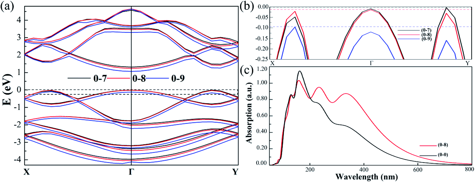 | ||
| Fig. 8 (a) The band structures of monolayer SnS with compressive strain (7–9%) along b direction. The black, red and blue lines denote the (0, −7%), (0, −8%) and (0, −9%) cases respectively. The VBM at Fermi level are shown in (b). The optical properties results: the calculation absorption curve of (0, 0) and (0, −8) for monolayer SnS in (c). | ||
4. Conclusion
This work presents a few properties of SnS monolayer under ununiformed strain beyond the axis, including structural transformation, metal/semiconductor transition, indirect/direct transition and negative poisson's ratio. The result suggested that the coupling effect of strain might play an important role in the properties detective of flexible materials and the SIPES and SIBP methods was a useful method to analysis the strain effect on layered materials. Our work also prove that the strain effect is a useful way to modulate the electronic and optic properties for low dimensional flexible material.Acknowledgements
The authors acknowledge the financial support from the National Natural Science Foundation of China (21573028, 21373281) the Program for New Century Excellent Talents in University (NCET-12-0587, NCET-13-0633). B. S. acknowledges the National Science Foundation Project of CQ CSTC, 020005303100 and Fundamental Research funds for the Central Universities for financial support.References
- G. R. Bhimanapati, Z. Lin, V. Meunier, Y. Jung, J. Cha, S. Das, D. Xiao, Y. Son, M. S. Strano, V. R. Cooper, L. Liang, S. G. Louie, E. Ringe, W. Zhou, S. S. Kim, R. R. Naik, B. G. Sumpter, H. Terrones, F. Xia, Y. Wang, J. Zhu, D. Akinwande, N. Alem, J. A. Schuller, R. E. Schaak, M. Terrones and J. A. Robinson, ACS Nano, 2015, 9, 11509–11539 CrossRef CAS PubMed.
- S. M. Yoon, H. J. Song and H. C. Choi, Adv. Mater., 2010, 22, 2164–2167 CrossRef CAS PubMed.
- D. D. Vaughn II, R. J. Patel, M. A. Hickner and R. E. Schaak, J. Am. Chem. Soc., 2010, 132, 15170–15172 CrossRef PubMed.
- R. Guo, X. Wang, Y. Kuang and B. Huang, Phys. Rev. B: Condens. Matter Mater. Phys., 2015, 92, 115202 CrossRef.
- R. Fei, W. Li, J. Li and L. Yang, Appl. Phys. Lett., 2015, 107, 173104 CrossRef.
- Y. Sun, Z. Zhong, T. Shirakawa, C. Franchini, D. Li, Y. Li, S. Yunoki and X.-Q. Chen, Phys. Rev. B: Condens. Matter Mater. Phys., 2013, 88, 235122 CrossRef.
- Y.-G. Guo, J.-S. Hu and L.-J. Wan, Adv. Mater., 2008, 20, 2878–2887 CrossRef CAS.
- Y. Chen, J. Wang, M. Zhang and Q. Zeng, RSC Adv., 2017, 7, 21221–21225 RSC.
- G. Shi and E. Kioupakis, Nano Lett., 2015, 15, 6926–6931 CrossRef PubMed.
- D. J. Xue, J. Tan, J. S. Hu, W. Hu, Y. G. Guo and L. J. Wan, Adv. Mater., 2012, 24, 4528–4533 CrossRef CAS PubMed.
- L. A. Burton, D. Colombara, R. D. Abellon, F. C. Grozema, L. M. Peter, T. J. Savenije, G. Dennler and A. Walsh, Chem. Mater., 2013, 25, 4908–4916 CrossRef CAS.
- J. Wang, F. Ma and M. Sun, RSC Adv., 2017, 7, 16801–16822 RSC.
- H. Wu, X. Liu, J. Yin, J. Zhou and W. Guo, Small, 2016, 12, 5276–5280 CrossRef CAS PubMed.
- J. Quereda, P. San-Jose, V. Parente, L. Vaquero-Garzon, A. J. Molina-Mendoza, N. Agrait, G. Rubio-Bollinger, F. Guinea, R. Roldan and A. Castellanos-Gomez, Nano Lett., 2016, 16, 2931–2937 CrossRef CAS PubMed.
- H. Y. Lv, W. J. Lu, D. F. Shao and Y. P. Sun, Phys. Rev. B: Condens. Matter Mater. Phys., 2014, 90, 173702 CrossRef.
- L. Huang, F. Wu and J. Li, J. Chem. Phys., 2016, 144, 114708 CrossRef PubMed.
- X. Peng, Q. Wei and A. Copple, Phys. Rev. B: Condens. Matter Mater. Phys., 2014, 90, 173702 CrossRef.
- W. Ju, T. Li, H. Wang, Y. Yong and J. Sun, Chem. Phys. Lett., 2015, 622, 109–114 CrossRef CAS.
- G. A. Tritsaris, B. D. Malone and E. Kaxiras, J. Appl. Phys., 2014, 115, 173702 CrossRef.
- N. Kerszberg and P. Suryanarayana, RSC Adv., 2015, 5, 43810–43814 RSC.
- Y. Wang, C. Cong, R. Fei, W. Yang, Y. Chen, B. Cao, L. Yang and T. Yu, Nano Res., 2015, 8, 3944–3953 CrossRef CAS.
- R. Fei and L. Yang, Nano Lett., 2014, 14, 2884–2889 CrossRef CAS PubMed.
- J. R. Brent, D. J. Lewis, T. Lorenz, E. A. Lewis, N. Savjani, S. J. Haigh, G. Seifert, B. Derby and P. O'Brien, J. Am. Chem. Soc., 2015, 137, 12689–12696 CrossRef CAS PubMed.
- F. Guinea, M. I. Katsnelson and A. K. Geim, Nat. Phys., 2009, 6, 30–33 CrossRef.
- S. S. Hegde, A. G. Kunjomana, K. A. Chandrasekharan, K. Ramesh and M. Prashantha, Phys. B, 2011, 406, 1143–1148 CrossRef CAS.
- A. J. Biacchi, D. D. Vaughn II and R. E. Schaak, J. Am. Chem. Soc., 2013, 135, 11634–11644 CrossRef CAS PubMed.
- M. Wu and X. C. Zeng, Nano Lett., 2016, 16, 3236–3241 CrossRef CAS PubMed.
- S. Z. Butler, S. M. Hollen, L. Cao, Y. Cui, J. A. Gupta, H. R. Gutierrez, T. F. Heinz, S. S. Hong, J. Huang, A. F. Ismach, E. Johnston-Halperin, M. Kuno, V. V. Plashnitsa, R. D. Robinson, R. S. Ruoff, S. Salahuddin, J. Shan, L. Shi, M. G. Spencer, M. Terrones, W. Windl and J. E. Goldberger, ACS Nano, 2013, 7, 2898–2926 CrossRef CAS PubMed.
- Y. Li, S. Yang and J. Li, J. Phys. Chem. C, 2014, 118, 23970–23976 CAS.
- G. Qin, Z. Qin, W. Z. Fang, L. C. Zhang, S. Y. Yue, Q. B. Yan, M. Hu and G. Su, Nanoscale, 2016, 8, 11306–11319 RSC.
- D. D. Cuong, S. H. Rhim, J.-H. Lee and S. C. Hong, AIP Adv., 2015, 5, 117147 CrossRef.
- K. K. Leung, W. Wang, H. Shu, Y. Y. Hui, S. Wang, P. W. K. Fong, F. Ding, S. P. Lau, C.-h. Lam and C. Surya, Cryst. Growth Des., 2013, 13, 4755–4759 CAS.
- K. T. Ramakrishna Reddy, N. Koteswara Reddy and R. W. Miles, Sol. Energy Mater. Sol. Cells, 2006, 90, 3041–3046 CrossRef CAS.
- P. D. Antunez, J. J. Buckley and R. L. Brutchey, Nanoscale, 2011, 3, 2399–2411 RSC.
- Z. Tian, C. Guo, M. Zhao, R. Li and J. Xue, ACS Nano, 2017, 11, 2219–2226 CrossRef CAS PubMed.
- B. D. Malone and E. Kaxiras, Phys. Rev. B: Condens. Matter Mater. Phys., 2013, 87, 245312 CrossRef.
- Z. Lu, S. Li, C. Liu, C. He, X. Yang, D. Ma, G. Xu and Z. Yang, RSC Adv., 2017, 7, 20398–20405 RSC.
- K.-H. Xue, L. R. C. Fonseca and X.-S. Miao, RSC Adv., 2017, 7, 21856–21868 RSC.
- S. Hao, V. P. Dravid, M. G. Kanatzidis and C. Wolverton, APL Mater., 2016, 4, 104505 CrossRef.
- W. Zhou and N. Umezawa, RSC Adv., 2017, 7, 20542–20547 RSC.
- M. M. Nassary, J. Alloys Compd., 2005, 398, 21–25 CrossRef CAS.
- H. Wei, Y. Su, S. Chen, Y. Lin, Z. Yang, X. Chen and Y. Zhang, J. Mater. Chem., 2011, 21, 12605 RSC.
- B. D. Malone, A. Gali and E. Kaxiras, Phys. Chem. Chem. Phys., 2014, 16, 26176–26183 RSC.
- A. K. Singh and R. G. Hennig, Appl. Phys. Lett., 2014, 105, 042103 CrossRef.
- A. Shafique and Y. H. Shin, Sci. Rep., 2017, 7, 506 CrossRef PubMed.
- C. Lee, X. Wei, J. W. Kysar and J. Hone, Science, 2008, 321, 385–388 CrossRef CAS PubMed.
- J. W. Jiang and H. S. Park, Nat. Commun., 2014, 5, 4727 CAS.
- A. S. Rodin, L. C. Gomes, A. Carvalho and A. H. Castro Neto, Phys. Rev. B, 2016, 93, 045431 CrossRef.
- L. A. Burton and A. Walsh, J. Phys. Chem. C, 2012, 116, 24262–24267 CAS.
- L. Li, Z. Chen, Y. Hu, X. Wang, T. Zhang, W. Chen and Q. Wang, J. Am. Chem. Soc., 2013, 135, 1213–1216 CrossRef CAS PubMed.
| This journal is © The Royal Society of Chemistry 2017 |