DOI:
10.1039/C7RA04472K
(Paper)
RSC Adv., 2017,
7, 34244-34250
Accurate analysis of the size distribution and crystallinity of boron doped Si nanocrystals via Raman and PL spectra
Received
21st April 2017
, Accepted 25th June 2017
First published on 7th July 2017
Abstract
A narrow size distribution of quantum dots (QDs) is needed for their application in photovoltaics but collection of such information is difficult. This paper demonstrates the application of Raman spectroscopy as a characterisation tool to extract the size distribution and crystalline fraction of Si QD samples fabricated through the sputter-anneal method. Measured Raman spectra of Si QD materials are de-convoluted into four components according to their origins and Raman scattering by Si QD cores is described by a modified one phonon confinement model, while other components are reproduced with Gaussian functions. Through fitting of Raman spectra, Si QD size distributions and Si crystalline fractions are obtained. The results are compared with the values extracted from PL modelling on a series of B doped Si QD samples. The good consistency between the values extracted by these two methods confirms the validity of the Raman model. The result confirms that Si crystallization has been suppressed by B doping as the average Si QD size and Si crystalline fraction are reduced with increased B doping level.
Introduction
Silicon quantum dots (Si QDs) embedded in an oxide or nitride matrix are considered to have high energy conversion efficiencies.1 To realize such efficient photonic devices, a tight control over size and a narrow size distribution are necessary. However, the size distribution of Si QDs embedded in a matrix is very difficult to obtain, considering their non-uniform shapes and remarkable difficulties in TEM imaging.2,3 Meanwhile, the optical characterization techniques such as PL and Raman spectroscopy are non-destructive and easily-performed but still lack quantitative analysis of the spectra. We proposed a method to accurately estimate the size distribution of such QDs from their photoluminescence (PL) spectra in previous work.4 The size distribution of nanoparticles from low frequency Raman scattering (LFRS) has been studied5–7 and in this paper high frequency Raman spectroscopy is introduced as another method to extract such information. Boron doping on Si QDs bilayers is studied by a combination of Raman and PL spectroscopies. Good agreement in term of the deduced Si QD size distribution has been obtained between these two methods.
Experimental details
Si QD bilayers with varied B doping power are prepared on fused-silica substrates through RF magnetron sputtering system in an argon atmosphere below 1.5 mTorr. Each of the samples consists of 30 bilayers, which are made of alternating SRO and SiO2 layers with respective thicknesses of 4 nm and 1.8 nm. The volume ratio of Si to SiO2 is controlled at 66% by adjusting the powers applied to the sputtered targets. In following discussions, samples are denoted as B0, B1, B2, B3, and B4, corresponding to B doping powers of 0 (intrinsic), 12.5, 25, 37.5, and 50 W respectively. Sample annealing is conducted in an 1100 °C N2 purged environment for 1 hour to facilitate Si QDs nucleation and growth.2 Annealed samples are characterized with Raman and PL spectroscopies respectively. In Raman measurement, an Ar-ion laser with wavelength of 514 nm is used as incident source without polarization. The diffraction grating of 1800 L mm−1 is selected, giving an instrumental resolution of 1.7 cm−1. The lens magnification (50×) and the exposure time (1 s for 10 times accumulations) adopted are delicately determined after several experiments in order to avoid additional Si crystallization and significant strains induced by a high laser power. The original power of the laser is 25 mW and drops to around 9.9 mW on sample after passing through the optics. The optical penetration depth is about 300 nm for a laser with 514 nm wavelength, covering the total thickness of samples fabricated in this work.8 In PL measurement, the intensity correction is made using a lamp with a calibrated spectra between 250 and 2400 nm. A laser diode with a wavelength of 405 nm is used as the excitation source in room temperature environment, and the PL signal is collected and analysed using a Si CCD camera cooled down to −30 °C.
Results and discussion
Fig. 1 is the high frequency Raman scattering obtained from annealed samples. Main Raman peaks, with different levels of downshifts, are identified near the bulk Si response at 520 cm−1 (labelled) in all samples, indicating the existence of crystalline Si.9 A one-phonon confinement model was developed by Richter et al.10 accounting for the size confinement effect. Assuming a spherical crystal with diameter D, the phonon is restricted to the volume of this crystallite, and as a result, the wave function can be expressed as:10–12| | |
ψ(q,r) = Fc(r,D)ɸ(q,r) = ψ′(q,r)u(q,r)
| (1) |
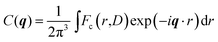
where u(q,r) has the periodicity of the lattice and Fc(r,D) is a phonon weighting/confinement function which can be expanded in Fourier integral as:| | |
Fc(r,D) = ∫C(q)exp(iq·r)dq
| (2) |
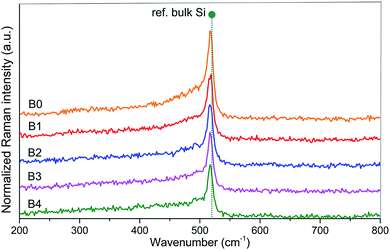 |
| | Fig. 1 Raman spectra for B doped samples. | |
Thus
| |
 | (3) |
Therefore, the first-order Raman spectrum of a nanocrystal can be calculated as:13
| |
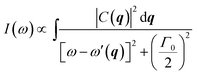 | (4) |
where
ω′(
q) is the phonon dispersion relation curve,
Γ0 the natural linewidth (
ΓSi = 3 cm
−1), and
a the lattice constant (
aSi = 0.543 nm) of the material.
The selection of the phonon confinement function Fc(r,D) and the integral range are two key parts of in eqn (4). Though the analytical form for Fc(r,D) can be arbitrary without significant physical reasons, in most case a Gaussian function shown in eqn (5) is adapted to characterize the Raman spectra of Si nanostructures.10,13
| |
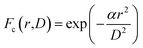 | (5) |
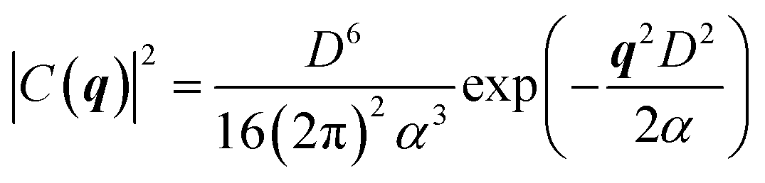
The corresponding Fourier coefficients are given by as:
| |
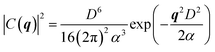 | (6) |
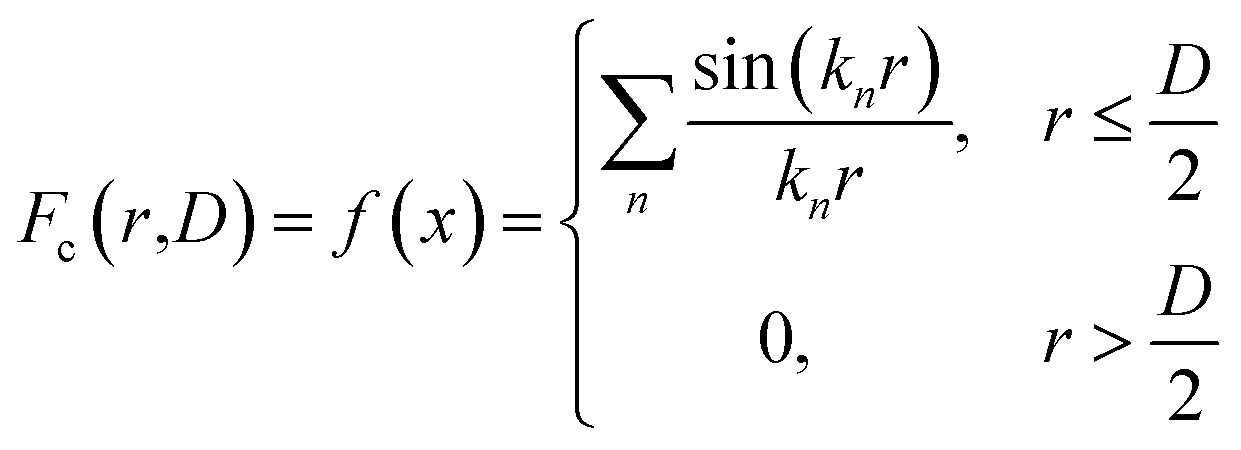
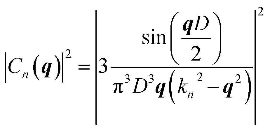
In eqn (5), α is a factor determining the degree of confinement, i.e. how quickly the wave function of phonon vanishes towards the boundary of a nanocrystal. In this case, the integral of eqn (5) is extended to the entire first Brillouin zone. However, Faraci et al.12 argued that this approach only observe a single-phonon wave vector, which was not realistic. They suggested a wave packet extended over the size of the nanocrystal; and in their modified model, a confinement function given by a weighted superposition of sinusoidal waves was tested.
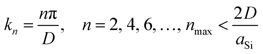
| |
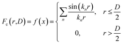 | (7) |
where
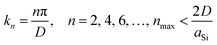
.
Thus, the corresponding Fourier coefficients are given by as:
| |
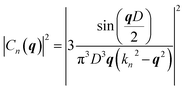 | (8) |
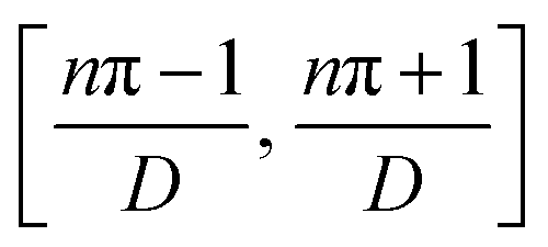
The form in eqn (7) has components centered at r = 0, which strongly attenuate to zero at the border of the nanocrystal.12 It is found that the first component of Fc(r,D) (i.e. n = 2) is the most appropriate for simulating the vibrational amplitude of the most Raman-active modes in a Si QD.12 In this modified approach, the phonon wave vectors q in eqn (7) that are contributing to the scattering process are limited to the range  due to the momentum conservation.12,14 This modification can give a good description of the vibrational confinement in Si spheres and a relatively good description of the Raman frequency shifts.13 Taking the Raman scattering efficiency
 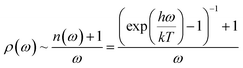 into account,14 the integral first-order Raman spectrum in eqn (4) can be rewritten as:12,14
| |
 | (9) |
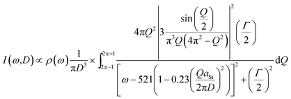
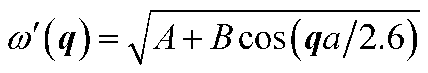
In eqn (9), the size dependency of the integral boundaries is removed with a change of variables. i.e. Q = qD.14 The common used analytical form of phonon dispersion curve ω′(q) for Si are 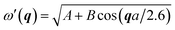 and
and 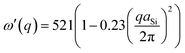 , respectively.15–17 But Faraci et al.12 has shown that notwithstanding the different analytical form, these two dispersion curves are very close in the common range of interest. Here we adopt the analytical form of
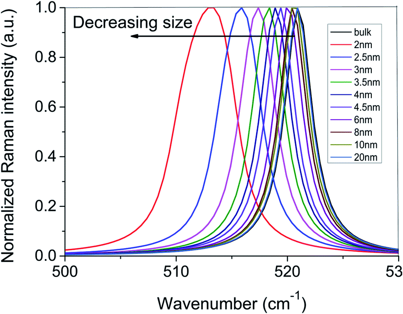
  for Si phonon dispersion relation in eqn (9). Fig. 2 demonstrates simulated Raman spectra for different sizes of Si nanocrystals. It is also noticeable that Raman response from Si nanocrystal with diameter of 20 nm is close to the one from bulk Si, and therefore it is safe to state that nanocrystal size larger than this value can be viewed as bulk Si behavior.
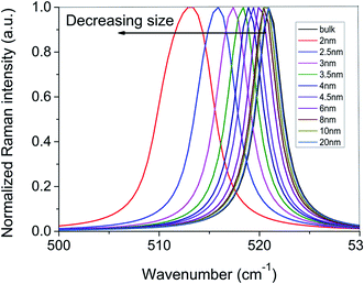 |
| | Fig. 2 Simulated Raman spectra (normalized) for varied sizes of Si nanocrystals using eqn (9). | |
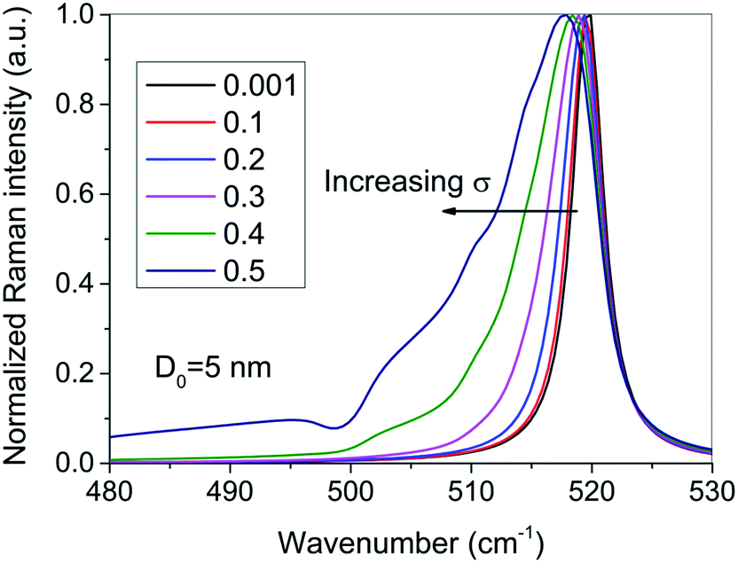
Eqn (9) enables experimental analysis of Si QD materials with a monodisperse distribution, i.e. uniform size. In reality, however, the size of fabricated Si nanocrystals is found to be spread out, which will make the Raman spectra more complicated. To account for this effect, eqn (9) is required to be projected onto the log-normal size distribution function that is integrated over the possible size range in the following way:18,19
| |
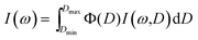 | (10) |
in which the log-normal size distribution with a mean size
D0 and a distribution skewness
σ is given as:
| |
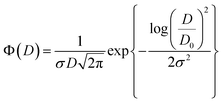 | (11) |
The effect of distribution skewness, or the degree of size dispersion, is simulated and displayed in Fig. 3. It is identified that as σ value increases, the Raman peak position is slightly moved towards the lower wave number while the asymmetry broadening of the spectra is significantly enhanced. This is because Si nanocrystals with smaller size tend to have higher Raman scattering efficiency according to the expression of ρ(ω) and thus their contributions to the final spectra become more obvious. It is also noticeable that as σ is approaching 1/10 of the value of mean size (i.e. σ = 0.4, 0.5), fringes appear in the spectra in the low wavenumber regime. This feature is a consequence of higher Raman scattering efficiency of smaller sized Si QD given in previous discussion.
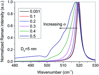 |
| | Fig. 3 Simulated Raman spectra (normalized) for Si nanocrystals with mean size D0 = 5 nm and different distribution skewness σ using eqn (10). | |
Apart from the size distribution caused effect, the amorphous Si phase has to be considered in the analysis of the Raman spectrum as well. Si QDs embedded in an amorphous matrix (either amorphous Si or dielectric material) tends to have a core–shell structure, in which the nanoscale Si crystalline core is surrounded by an outer shell.20,21 The outer shell consists of near-surface fine sized crystalline phases with irregular shapes, which gradually transits to amorphous Si phases (a-Si) before reaching the amorphous matrix.21–24 The presence of the near-surface crystalline phases manifests itself as a weak intermediate peak near 500–510 cm−1 in Raman spectrum. The a-Si phases are excess Si that is not crystallized after annealing. In terms of Raman spectroscopy, a-Si will introduce broad humps in the low wavenumber tail of the measured spectra, which include: (i) 300 cm−1 phase from the longitudinal acoustic (LA) vibration mode; (ii) 480 cm−1 phase from the transverse optical (TO) vibration mode.25 The existences of a-Si phases and near-surface states have important influences on both optical and electrical properties of the material. They are closely affected by material processing parameters, including material stoichiometry, annealing temperature and duration, and doping types and levels. In this paper, these phases will be reproduced with their corresponding Gaussian functions in Raman spectra simulations.
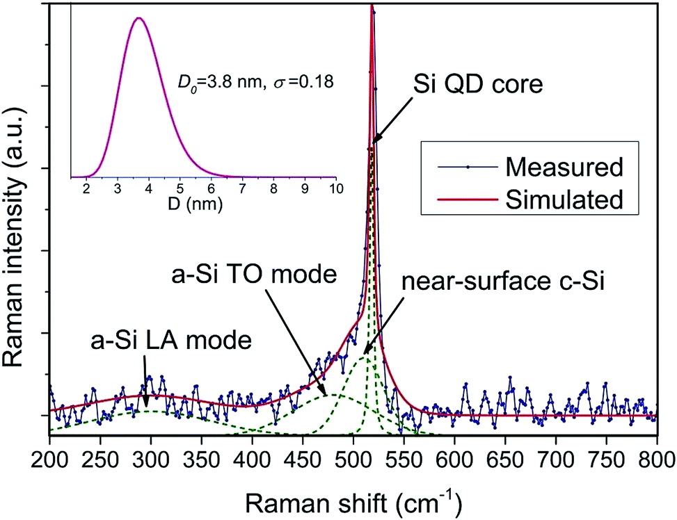
A typical deconvolution of Raman spectrum adapted in this paper is shown in Fig. 4. Under the assumption that the majority of Si QD is hard sphere in shape, the response from c-Si QD cores in the vicinity of 520 cm−1 is fitted with the modified one-phonon confinement model. The intermediate peak from near-surface crystalline states around 510 cm−1 is reproduced using a Gaussian function. As pointed out above, though these states are also crystalline Si components, they are prone to have irregular shapes instead of spheres. This will introduce complicated modifications to the weighing function if the one-phonon confinement model is employed to fit their Raman responses. Therefore, for simplicity, a Gaussian function is applied instead. Apart from c-Si responses, the two a-Si phases near 300 cm−1 and 480 cm−1 are reproduced by their corresponding Gaussian functions, which is a widely adapted method in other researches.22–24 In the rest parts of this paper, Raman spectrum analysis will all be based on the simulation process described above.
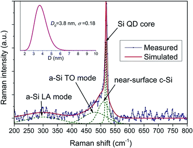 |
| | Fig. 4 A typical deconvolution of Raman spectrum: The spectrum consists a c-Si phase that originates from Si QD core in the vicinity of 520 cm−1, two a-Si phases from LA mode and TO mode near 300 cm−1 and 480 cm−1, respectively, an intermediate phase due to near-surface c-Si near 510 cm−1. The inset demonstrates the log-normal size distribution for Si QDs extracted from simulation of the Raman spectrum. | |
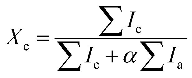
Using the modified one-phonon confinement model, the log-normal size distribution function of Si QDs can be extracted by adjusting the mean size D0 and distribution skewness σ, see inset of Fig. 4. The crystalline fraction Xc of Si with respect to a-Si can be estimated through eqn (12).24,26
| |
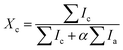 | (12) |
in which ∑
Ic and ∑
Ia are sums of integrated intensities for c-Si (
i.e. 518 cm
−1 and 510 cm
−1 peaks in
Fig. 4), and a-Si (
i.e. 300 cm
−1 and 480 cm
−1 peaks in
Fig. 4) profiles respectively, and
α = 0.1 due to the silicon content used.
26,27
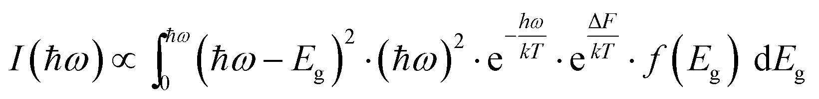
To verify the validity of extracting Si QDs size distribution information from Raman simulation, a model is introduced and used to fit PL spectrum for the same purpose. This PL model correlates the breadth of PL emission with the size distribution of Si QDs, which in return is manifested as distribution of energy bandgaps.4 Thus the PL intensity as a function of energy ℏω is expressed in eqn (13):4
| |
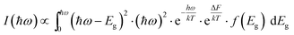 | (13) |
where
k is the Boltzmann constant, and
Eg is energy bandgap. Δ
F =
EFn −
EFp with
EFn and
EFp correspond to quasi-Fermi energies for electrons and holes respectively.
f(
Eg) is the probability density function of the energy bandgaps. Again, a log-normal function in
eqn (11) is adapted for Si QDs size distribution, then
f(
Eg) is given by
eqn (14).
4| |
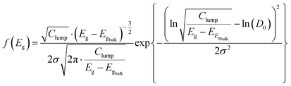 | (14) |
in which
Egbulk is the energy bandgap of bulk Si, and
Clump = 2 eV nm
2 is a coefficient lumping all other parameters that account for quantum confinement effect.
28 Similarly, size distribution of Si QDs can be obtained through simulation of the PL profile. With this alternative approach, it is possible to support conclusions from Raman simulation described previously.
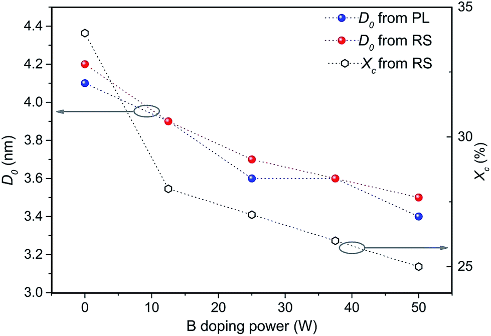
PL spectra of all samples are demonstrated in our previous work.29 The intensity of PL response initially increases from intrinsic sample (B0) to lightly doped sample (B1), which is followed by a decrease in intensity as the doping power further increases (B2–B4). Simultaneously, the PL peak position is slightly blue-shifted from intrinsic sample to doped samples. Assuming the maxima of the PL profiles are responses from Si QDs, such shifts indicate changes in energy bandgap due to evolution of Si QDs size distributions altered by B doping. Si QDs size distributions extracted through simulations of PL spectra are summarized in Table 1.
Table 1 Summary of simulation results of Raman and PL spectroscopies
| Samples |
Xc |
Si QDs size distribution from Raman |
Si QDs size distribution from PL |
| D0 (nm) |
σ |
D0 (nm) |
σ |
| B0 |
34% |
4.2 |
0.43 |
4.1 |
0.54 |
| B1 |
28% |
3.9 |
0.40 |
3.9 |
0.51 |
| B2 |
27% |
3.7 |
0.39 |
3.6 |
0.51 |
| B3 |
26% |
3.6 |
0.35 |
3.6 |
0.52 |
| B4 |
25% |
3.5 |
0.35 |
3.4 |
0.54 |
According to Fig. 5, extracted values for Si QDs average size from Raman and PL simulations are in good consistency with each other. In general, when the B doping power is increased, the average Si QDs size gets smaller. The crystalline fraction Xc plotted in the same diagram also demonstrates a reducing trend when B doping level is enhanced. Both of the changes imply the suppression of Si crystallization by B doping. Similar effect has been reported and discussed by Hao et al.,30 in which they attributed this inhibited Si crystallization to the impurity induced local deformations.
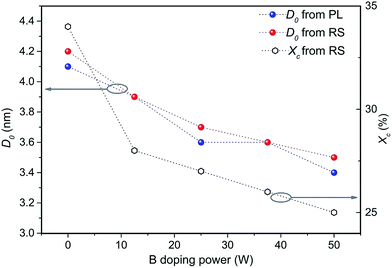 |
| | Fig. 5 Extracted Si QDs average sizes and crystalline fractions from Raman and PL simulations versus B doping power. | |
In Table 2, σ values obtained from Raman simulations are lower than those from PL simulations for each sample. This discrepancy can be explained in two aspects. Firstly, the full width half maximum (FWHM) of simulated c-Si peak using the modified one-phonon confinement model are smaller than those of the measured Raman spectra, see Table 2. Though the level of size dispersion (i.e. σ value) has little effect on the calculated Raman frequency shift, it has great influence on the width and the shape of the Raman spectra.31 Therefore, lower values of deducted FWHM indicate possible underestimations of σ from Raman simulations. This is because the Gaussian function for the intermediate peak (near-surface crystalline phases) also contributes to the FWHM of the final simulated Raman profile, however, its size information is not accounted. Secondly, in PL simulations, the model employed here takes into consideration of all radiative recombination processes regardless of their actual origins. Since it is not easy to de-convolute emissions of defect states from those of Si QDs, the level of Si QDs size dispersion (i.e. σ values) extracted in PL simulations can be overestimated to some extent. Additionally, the aforementioned near-surface states, which are excluded from the one-phonon confinement model in Raman simulations, may cause exciton localization and thus can be PL active.21,32 As a consequence, the size information these states contain may be included in PL simulations similar to defect-related emissions. Therefore, a σ in between the range of Raman and PL extracted values can be a reasonable good approximation of Si QDs size distribution skewness.
Table 2 Comparison of FWHM of simulated c-Si peaks and measured peaks
| Samples |
FWHM of simulated c-Si peak (cm−1) |
FWHM of measured peak (cm−1) |
| B0 |
10.1 |
13.5 |
| B1 |
9.7 |
13.8 |
| B2 |
9.1 |
13.8 |
| B3 |
8.9 |
11.3 |
| B4 |
8.3 |
11.3 |
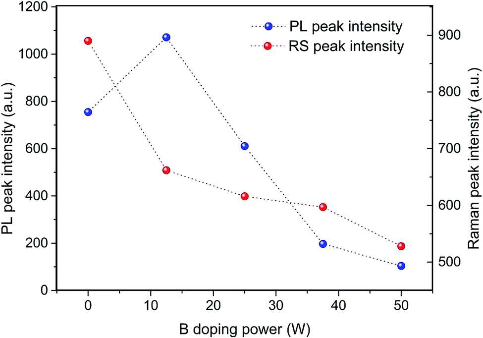
Fig. 6 compares the evolution of relative intensities of Raman and PL peaks as a function of B doping power. To clarify, intensities shown on the graph were average results. According to the experiments, measurement errors for Raman spectra with detected peak intensity around 100 counts were within 6% of the average value; while for PL with peak intensity around 100 counts, the values were less than 10% of the average. Measurement result tends to become more converged as the detected intensity gets higher and thus the error range narrows. Therefore, for the detected intensity levels in both Raman and PL spectra demonstrated here, error bars are not illustrated in Fig. 6 due to their relatively small magnitudes compared to the measurement values. In Raman measurement, the intrinsic sample shows the strongest response. With additions of B dopants, the obtained peak intensity decreases. Under the identical measurement conditions and equipment setups, this tendency, on one hand, is associated with the reduction of Raman scattering volumes due to the decreased Si QDs sizes by increased B doping levels;33 and on the other hand, is due to the lowered concentration of c-Si vibrational modes caused by decreased Si crystalline fractions according to Fig. 5.34 The relative intensity of PL peak in Fig. 6 is initially enhanced from sample B0 to B1, which is then reduced when the B doping level further increases (B2–B4). It is verified that the improved PL peak intensity in lightly doped sample (B1) is a result of B passivation effect to a-Si dangling bonds.29 When the B doping level continues to increase, both Auger recombination and impurity induced strains (which will add to non-radiative recombination canters) are enhanced simultaneously.29 As a combined result, PL emissions are quenched in samples B2–B4.
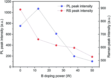 |
| | Fig. 6 Comparison of PL and Raman peak intensities as a function of B doping power. | |
To conclude, Si QDs average sizes extracted from Raman and PL simulations demonstrate consistent results. It is observed that extracted size distribution skewness from Raman modelling is underestimated, while the one from PL modelling is overestimated. Therefore, a value between them can be considered a good description of size dispersion level. Both of Raman and PL spectroscopies verify that Si crystallization has been supressed by B doping as average Si QDs size and Si crystalline fraction are reduced with increased B doping level. The decreasing Raman peak intensity with B doping power is caused by reduction in both the scattering volume in smaller Si QDs, and the available vibrational modes. On the other hand, an increase of PL peak intensity is identified when Si QDs are slightly doped, which is benefited from B passivation effect. Further improvement of B doping level leads to reduced PL peak intensities as a result of enhanced Auger process and other non-radiative recombination.
Conclusion
This paper demonstrates the application of Raman spectroscopy as a characterization tool to extract the size distribution and crystalline fraction of Si QD samples fabricated through sputter-anneal method. Basic principles of Raman spectroscopy and its application in crystalline materials, including both perfect and imperfect crystals, are introduced. Measured Raman spectra of Si QD materials are de-convoluted into four components according to their origins. Raman scattering by Si QD core is described by a modified one-phonon confinement model, while other components are reproduced with Gaussian functions. Through fitting of Raman spectra, Si QDs size distributions and Si crystalline fractions are obtained. The results are compared with the values extracted from PL modelling on a series of B doped Si QD samples. The good consistency between the values extracted by these two methods confirms the validity of the Raman model developed in this paper.
Acknowledgements
This Program has been supported by the Australian Government through the Australian Renewable Energy Agency (ARENA). Responsibility for the views, information or advice expressed herein is not accepted by the Australian Government. The work in China is supported by National Natural Science Foundation of China (Grant No. 51335002).
References
- G. Conibeer, M. Green, R. Corkish, Y. Cho, E.-C. Cho and C.-W. Jiang, et al., Silicon nanostructures for third generation photovoltaic solar cells, Thin Solid Films, 2006, 511–512, 654–662 CrossRef CAS.
- M. Zacharias, J. Heitmann, R. Scholz, U. Kahler, M. Schmidt and J. Bläsing, Size-controlled highly luminescent silicon nanocrystals: a SiO/SiO2 superlattice approach, Appl. Phys. Lett., 2002, 80(4), 661–663 CrossRef CAS.
- L. F. Kourkoutis, X. Hao, S. Huang, B. Puthen-Veettil, G. Conibeer and M. A. Green, et al., Three-dimensional imaging for precise structural control of Si quantum dot networks for all-Si solar cells, Nanoscale, 2013, 5(16), 7499–7504 RSC.
- X. Jia, P. Zhang, Z. Lin, R. Anthony, U. Kortshagen and S. Huang, et al., Accurate determination of the size distribution of Si nanocrystals from PL spectra, RSC Adv., 2015, 5(68), 55119–55125 RSC.
- V. Mankad, K. Mishra, S. K. Gupta, T. Ravindran and P. K. Jha, Low frequency Raman scattering from confined acoustic phonons in freestanding silver nanoparticles, Vib. Spectrosc., 2012, 61, 183–187 CrossRef CAS.
- S. K. Gupta, S. Sahoo, P. K. Jha, A. Arora and Y. Azhniuk, Observation of torsional mode in CdS1−xSex nanoparticles in a borosilicate glass, J. Appl. Phys., 2009, 106(2), 024307 CrossRef.
- M. Ivanda, A. Hohl, M. Montagna, G. Mariotto, M. Ferrari and Z. Crnjak Orel, et al., Raman scattering of acoustical modes of silicon nanoparticles embedded in silica matrix, J. Raman Spectrosc., 2006, 37(1–3), 161–165 CrossRef CAS.
- J. Song, C. Yang, H. Hu, X. Dai, C. Wang and H. Zhang, Penetration depth at various Raman excitation wavelengths and stress model for Raman spectrum in biaxially-strained Si, Sci. China: Phys., Mech. Astron., 2013, 56(11), 2065–2070 CrossRef CAS.
- J. Zi, H. Büscher, C. Falter, W. Ludwig, K. Zhang and X. Xie, Raman shifts in Si nanocrystals, Appl. Phys. Lett., 1996, 69(2), 200–202 CrossRef CAS.
- H. Richter, Z. P. Wang and L. Ley, The one phonon Raman spectrum in microcrystalline silicon, Solid State Commun., 1981, 39(5), 625–629 CrossRef CAS.
- I. H. Campbell and P. M. Fauchet, The effects of microcrystal size and shape on the one phonon Raman spectra of crystalline semiconductors, Solid State Commun., 1986, 58(10), 739–741 CrossRef CAS.
- G. Faraci, S. Gibilisco, P. Russo, A. R. Pennisi and S. La Rosa, Modified Raman confinement model for Si nanocrystals, Phys. Rev. B: Condens. Matter Mater. Phys., 2006, 73(3), 033307 CrossRef.
- J. Zi, K. Zhang and X. Xie, Comparison of models for Raman spectra of Si nanocrystals, Phys. Rev. B: Condens. Matter Mater. Phys., 1997, 55(15), 9263–9266 CrossRef CAS.
- İ. Doğan and M. C. M. van de Sanden, Direct characterization of nanocrystal size distribution using Raman spectroscopy, J. Appl. Phys., 2013, 114(13), 134310 CrossRef.
- S. K. Gupta and P. K. Jha, Modified phonon confinement model for size dependent Raman shift and linewidth of silicon nanocrystals, Solid State Commun., 2009, 149(45), 1989–1992 CrossRef CAS.
- V. Paillard, P. Puech, M. Laguna, R. Carles, B. Kohn and F. Huisken, Improved one-phonon confinement model for an accurate size determination of silicon nanocrystals, J. Appl. Phys., 1999, 86(4), 1921–1924 CrossRef CAS.
- R. Tubino, L. Piseri and G. Zerbi, Lattice dynamics and spectroscopic properties by a valence force potential of diamondlike crystals: C, Si, Ge, and Sn, J. Chem. Phys., 1972, 56(3), 1022–1039 CrossRef CAS.
- R. Espiau de Lamaëstre and H. Bernas, Significance of lognormal nanocrystal size distributions, Phys. Rev. B: Condens. Matter Mater. Phys., 2006, 73(12), 125317 CrossRef.
- L. B. Kiss, J. Söderlund, G. A. Niklasson and C. G. Granqvist, New approach to the origin of lognormal size distributions of nanoparticles, Nanotechnology, 1999, 10(1), 25 CrossRef.
- S. Hernández, A. Martínez, P. Pellegrino, Y. Lebour, B. Garrido and E. Jordana, et al., Silicon nanocluster crystallization in SiOx films studied by Raman scattering, J. Appl. Phys., 2008, 104(4), 044304 CrossRef.
- X. L. Wu, G. G. Siu, S. Tong, X. N. Liu, F. Yan and S. S. Jiang, et al., Raman scattering of alternating nanocrystalline silicon/amorphous silicon multilayers, Appl. Phys. Lett., 1996, 69(4), 523–525 CrossRef CAS.
- D. D. Tuschel and J. P. Lavine, Micro-Raman Characterization of Unusual Defect Structure in Arsenic-Implanted Silicon, MRS Online Proc. Libr., 1999, 588 DOI:10.1557/PROC-588-227.
- T. Kaneko, M. Wakagi, O. Ki and T. Minemura, Change in crystalline morphologies of polycrystalline silicon films prepared by radio-frequency plasma-enhanced chemical vapor deposition using SiF4 + H2 gas mixture at 350
![[thin space (1/6-em)]](https://www.rsc.org/images/entities/char_2009.gif) °C, Appl. Phys. Lett., 1994, 64(14), 1865–1867 CrossRef CAS.
°C, Appl. Phys. Lett., 1994, 64(14), 1865–1867 CrossRef CAS. - L. Houben, M. Luysberg, P. Hapke, R. Carius, F. Finger and H. Wagner, Structural properties of microcrystalline silicon in the transition from highly crystalline to amorphous growth, Philos. Mag. A, 1998, 77(6), 1447–1460 CAS.
- A. T. Voutsas, M. K. Hatalis, J. Boyce and A. Chiang, Raman spectroscopy of amorphous and microcrystalline silicon films deposited by low-pressure chemical vapor deposition, J. Appl. Phys., 1995, 78(12), 6999–7006 CrossRef CAS.
- C. Becker, F. Ruske, T. Sontheimer, B. Gorka, U. Bloeck and S. Gall, et al., Microstructure and photovoltaic performance of polycrystalline silicon thin films on temperature-stable ZnO:Al layers, J. Appl. Phys., 2009, 106(8), 084506 CrossRef.
- T. Zhang, B. Simonds, K. Nomoto, B. P. Veettil, Z. Lin and I. P. Wurfl, et al., Pulsed KrF excimer laser dopant activation in nanocrystal silicon in a silicon dioxide matrix, Appl. Phys. Lett., 2016, 108(8), 083103 CrossRef.
- G. Conibeer, M. A. Green, D. König, I. Perez-Wurfl, S. Huang and X. Hao, et al., Silicon quantum dot based solar cells: addressing the issues of doping, voltage and current transport, Prog. Photovoltaics, 2011, 19(7), 813–824 CAS.
- B. Puthen Veettil, L. Wu, X. Jia, Z. Lin, T. Zhang and T. Yang, et al., Passivation effects in B doped self-assembled Si nanocrystals, Appl. Phys. Lett., 2014, 105(22), 222108 CrossRef.
- X. J. Hao, E. C. Cho, C. Flynn, Y. S. Shen, S. C. Park and G. Conibeer, et al., Synthesis and characterization of boron-doped Si quantum dots for all-Si quantum dot tandem solar cells, Sol. Energy Mater. Sol. Cells, 2009, 93(2), 273–279 CrossRef CAS.
- W. Ke, X. Feng and Y. Huang, The effect of Si-nanocrystal size distribution on Raman spectrum, J. Appl. Phys., 2011, 109(8), 083526 CrossRef.
- Y. Kanemitsu, S. Okamoto, M. Otobe and S. Oda, Photoluminescence mechanism in surface-oxidized silicon nanocrystals, Phys. Rev. B: Condens. Matter Mater. Phys., 1997, 55(12), R7375–R7378 CrossRef CAS.
- S. Hernández, J. López-Vidrier, L. López-Conesa, D. Hiller, S. Gutsch and J. Ibáñez, et al., Determining the crystalline degree of silicon nanoclusters/SiO2 multilayers by Raman scattering, J. Appl. Phys., 2014, 115(20), 203504 CrossRef.
- I. R. Lewis and H. Edwards, Handbook of Raman Spectroscopy: From the Research Laboratory to the Process Line, CRC Press, 2001 Search PubMed.
|
| This journal is © The Royal Society of Chemistry 2017 |
Click here to see how this site uses Cookies. View our privacy policy here. 
 Open Access Article
 This Open Access Article is licensed under a Creative Commons Attribution-Non Commercial 3.0 Unported Licence
 *ab,
Z. Lin*b,
T. Zhangb,
B. Puthen-Veettilb,
T. Yang
*ab,
Z. Lin*b,
T. Zhangb,
B. Puthen-Veettilb,
T. Yang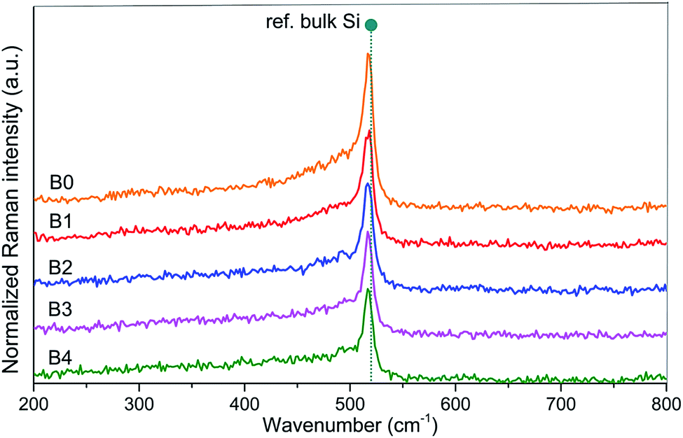


 .
.
 due to the momentum conservation.12,14 This modification can give a good description of the vibrational confinement in Si spheres and a relatively good description of the Raman frequency shifts.13 Taking the Raman scattering efficiency
  into account,14 the integral first-order Raman spectrum in eqn (4) can be rewritten as:12,14
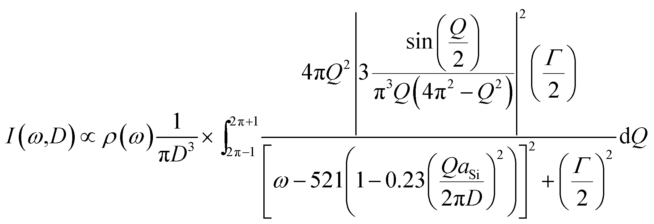
 and
and 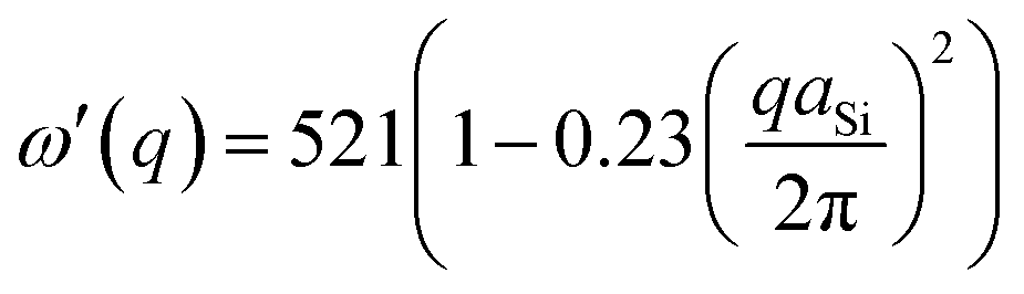 , respectively.15–17 But Faraci et al.12 has shown that notwithstanding the different analytical form, these two dispersion curves are very close in the common range of interest. Here we adopt the analytical form of
 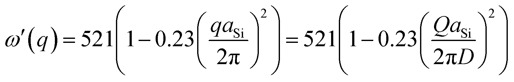 for Si phonon dispersion relation in eqn (9). Fig. 2 demonstrates simulated Raman spectra for different sizes of Si nanocrystals. It is also noticeable that Raman response from Si nanocrystal with diameter of 20 nm is close to the one from bulk Si, and therefore it is safe to state that nanocrystal size larger than this value can be viewed as bulk Si behavior.