
 Open Access Article
 This Open Access Article is licensed under a
 Creative Commons Attribution 3.0 Unported Licence
Metal-catalyst-free growth of graphene on insulating substrates by ammonia-assisted microwave plasma-enhanced chemical vapor deposition
Shan Zheng,
Guofang Zhong *,
Xingyi Wu,
Lorenzo D'Arsiè and
John Robertson
*,
Xingyi Wu,
Lorenzo D'Arsiè and
John Robertson
Department of Engineering, University of Cambridge, Cambridge CB2 1PZ, UK. E-mail: gz222@cam.ac.uk; Tel: +44 (0) 1223 748317
First published on 30th June 2017
Abstract
We study the metal-catalyst-free growth of uniform and continuous graphene films on different insulating substrates by microwave plasma-enhanced chemical vapor deposition (PECVD) with a gas mixture of C2H2, NH3, and H2 at a relatively low temperature of 700–750 °C. Compared to growth using only C2H2 and H2, the use of NH3 during synthesis is found to be beneficial, in transforming vertical graphene nano-walls into a layer-by-layer film, reducing the density of defects, and improving the graphene quality. The effect of different insulating substrates (including Al2O3 and SiO2) on the growth of graphene was studied under different growth temperatures, implying that the growth-temperature window and catalytic effect vary among insulators. The low activation energy barrier of Al2O3 proves it to be a more suitable substrate for the metal-catalyst-free growth of graphene at low temperature. These directly grown graphene films on insulators can be conveniently integrated into various electronic and optoelectronic applications avoiding any post-growth transfer processes.
1. Introduction
Graphene is a two-dimensional, single-layer sheet of sp2-bonded carbon atoms packed into a honeycomb lattice. It has been regarded as one of the most attractive candidates for future electrical and optical applications owing to its excellent properties such as high carrier mobility, optical transparency, mechanical flexibility, and high thermal conductivity.1,2 To fully realize its potential in real-world devices, metal-catalyst chemical vapor deposition (CVD) has been widely used in the large-scale, high-quality and cost-effective synthesis of graphene. However, this method has significant limitations in that the growth is normally carried out at ∼1000 °C,3–8 on a metal catalyst and requires a post-growth transfer process from metal onto an insulating substrate to make the device. The difficult transfer process usually results in polymer or metal residues, and wrinkling or breakage of graphene.9–11 Therefore, it would be a great advantage to develop a direct, metal-free growth method of graphene onto insulating substrates at low temperature.Unfortunately, insulating substrates generally display weak catalytic nature. The principle role of the catalyst in graphene growth is to dehydrogenate the precursor species12 and to chemisorb the hydrocarbon as a mobile surface species to cluster into the growing graphene grains. Some oxides such as VOx and Cr2O3 can act as dehydrogenation catalysts. The stability of strongly bonded oxides such as ZrO2 or HfO2 against reduction by carbon and have been used to grow carbon nano structures.13–16 There is also the novel idea of using remote copper or iron based catalysts which are then volatilized after the graphene growth.17 Nevertheless, the direct growth of graphene onto insulating substrates has been frequently tried and tends to show degraded quality compared with those grown on metals.18 In order to overcome the large energy barrier for graphene nucleation without metal catalysts,19 even higher temperatures (1065–1650 °C) are required by thermal CVD to obtain graphene to compete with the metal-catalyzed growth.20–24
To lower the growth temperature, it is useful to consider plasma-enhanced chemical vapor deposition (PECVD).25 The presence of energetic electrons, excited molecules/atoms, and free radicals generated in the plasma region can promote the decomposition of reactant gases, thus partly compensating for the weak catalytic nature of insulating substrates.26 Several PECVD studies have been reported on SiO2,27–38 quartz,27,31,38 glass,34,39 and Al2O3![[thin space (1/6-em)]](https://www.rsc.org/images/entities/char_2009.gif) 28,38 to explore the synthesis of graphene without metal catalysts at low temperature. Successful enlargement of isolated grain sizes has been realized using two-step growth in PECVD process.27–30 However, extremely long growth times (over 9 hours)27 or high-temperature pre-annealing (1000 °C)29 was still needed to obtain isolated grains, and high mobility values were only measured on single grain devices due to discontinuous films.28–30 Other groups tried to grow continuous graphene using PECVD. However, these films suffered from common problems such as many defects, less surface uniformity,31–39 and three-dimensional (3D) nano-wall growth.31,34,37,40 All these drawbacks have limited graphene from fulfilling its excellent electrical properties and developing its advantage of atomic thickness. Therefore, a continuous, uniform, and two-dimensional graphene film with a low defect density is desirable, which can enable graphene integrated with the modern silicon electronics as well as other two-dimensional materials like transition metal dichalcogenides.
28,38 to explore the synthesis of graphene without metal catalysts at low temperature. Successful enlargement of isolated grain sizes has been realized using two-step growth in PECVD process.27–30 However, extremely long growth times (over 9 hours)27 or high-temperature pre-annealing (1000 °C)29 was still needed to obtain isolated grains, and high mobility values were only measured on single grain devices due to discontinuous films.28–30 Other groups tried to grow continuous graphene using PECVD. However, these films suffered from common problems such as many defects, less surface uniformity,31–39 and three-dimensional (3D) nano-wall growth.31,34,37,40 All these drawbacks have limited graphene from fulfilling its excellent electrical properties and developing its advantage of atomic thickness. Therefore, a continuous, uniform, and two-dimensional graphene film with a low defect density is desirable, which can enable graphene integrated with the modern silicon electronics as well as other two-dimensional materials like transition metal dichalcogenides.
When it comes to device fabrication, insulators serve as gates in field-effect transistors (FETs), which have a strong influence on fulfilling the properties of graphene. However, the weak catalysis of insulators makes the selection of more proper insulating substrates essential in the metal-catalyst-free growth of graphene. SiO2 might not be an ideal substrate for graphene FETs, because the high interface states density and impurity-induced trapped charges on SiO2 substrates could cause carrier scattering issues that limit the performance of devices.41 Recent studies suggest that using high dielectric constant (high-κ) materials like Al2O3 as gate insulators would boost the performance of devices due to the reduction of Coulomb scattering in graphene owing to the dielectric screening effect.42 Therefore, the direct assembly of graphene on high-κ dielectrics would be useful. Atomic layer deposition (ALD) is a typical technique to obtain high-quality, thickness-controlled, pinhole-free high-κ thin films, which could provide a smooth and continuous surface for the graphene growth.43 Furthermore, the graphene/high-κ dielectric structure could be easily applied onto any semiconductor or substrate for functional device fabrications. However, the only attempt of metal-catalyst-free PECVD growth of graphene on atomic layer deposited Al2O3 substrates38 faced all the common problems mentioned above such as a high density of defects and multi-layer structures, but factors that degraded the quality and the mechanism behind it are not very clear.
Here, we demonstrate the metal-catalyst-free growth of graphene on SiO2 and Al2O3 by PECVD to investigate the possible solutions to reduce the density of defects and 3D nano-walls. By decreasing the concentration of the carbon gas and especially introducing NH3 in the growth, continuous and uniform graphene film with a low density of defects and no 3D nano-walls can be synthesized in our microwave PECVD system, thus the quality of graphene has been improved. Moreover, the graphene films produced on SiO2 and Al2O3 under different growth temperatures have been compared, which can offer a better understanding of the weak catalytic effect of different insulating substrates on the graphene growth.
2. Experimental
The low-temperature growth of graphene on various insulators was carried out in a homemade microwave (2.45 GHz) PECVD system using reactant gases including C2H2, NH3, and H2, as schematically shown in Fig. 1a. Dielectric substrates were placed on a PBN/PG (Pyrolytic Boron Nitride/Pyrolytic Graphite) heater element enclosed in a metal cage with a honeycomb mesh shield, as shown in the zoom-in image (Fig. 1b). This configuration can protect the samples from the ion-induced damage of the plasma ball, while the energetic and reactive species could pass through the mesh shield and reach the substrates to synthesize graphene. First, insulating substrates were heated to 650–750 °C after pumping down the chamber to 1 × 10⁻⁶ mbar. Second, H2 was introduced at a rate of 400 sccm and a microwave plasma was ignited above the metal cage at a pressure of 15 mbar and a power of 600 W for 10 min. Third, C2H2, or C2H2 and NH3 were added to the H2 flow to start the graphene growth. The total gas flow rate was kept at 400 sccm (C2H2: 20–40 sccm, NH3: 0–120 sccm, and H2: 240–360 sccm). Finally, after three-hour growth, samples were cooled down by switching off the C2H2 and NH3 flow, the plasma, and the heater power supply.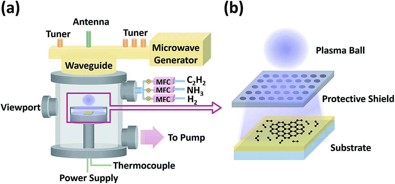 | ||
| Fig. 1 Schematic illustrations of (a) the homemade microwave plasma-enhanced chemical vapor deposition system and (b) the zoom-in image of the graphene growth process. | ||
High-κ dielectric Al2O3 was deposited on SiO2 (300 nm)/p-Si wafer via ALD. Before the ALD process, all the wafers were cleaned by sonication in acetone, isopropyl alcohol, and de-ionized water, and then dried with N2. The cleaned wafers were placed in the chamber of Savannah S200 ALD reactor at the temperature of 200 °C with N2 introduced as both carrier gas and purge gas. H2O was used as the oxidant precursor, and trimethylaluminium (TMA) was the metal precursor for the deposition of Al2O3 dielectric surface. By changing the number of growth cycles, high-κ thin film was obtained with thicknesses of 3 nm measured by ellipsometry. Besides Al2O3, SiO2 (300 nm)/p-Si substrates were used as the control group in the graphene growth. Other insulating substrates were also tested in our experiments to investigate the effect of insulating substrates on the graphene growth, including sapphire, quartz, MnO2 spin coated on SiO2 substrates, HfO2 and TiO2 deposited on SiO2 substrates via ALD.
Several characterization techniques were used to investigate the quality and properties of the synthesized graphene. The surface morphology was observed by scanning electron microscopy (SEM, Carl Zeiss SIGMA, 1 kV), atomic force microscopy (AFM, Agilent 5500) and optical microscopy (Nikon ECLIPSE LV150N). The thicknesses of insulators were measured by ellipsometer (Gaertner L117). Raman spectroscopy (Renishaw InVia spectrometer, 457 nm excitation) was used to measure the crystallinity of graphene. Electrical properties were measured by a standard four-probe method (Keithley 4200-SCS Semiconductor Characterization System) at room temperature.
3. Results and discussion
We first tried to grow graphene by microwave PECVD using H2 and C2H2. It is found that 3D graphene commonly appears on both SiO2 and Al2O3 substrates at high C2H2 volume concentrations. However by decreasing the concentration of C2H2 from 10% to 5%, 3D nano-walls can be greatly reduced on both substrates as shown in the left column (the blue area) in Fig. 2. PECVD assisted growth of graphene can be regarded as the competing result of graphene nucleation and growth due to the saturation of hydrocarbon precursors and the etching of carbon by atomic hydrogen. The abundant carbon source results in repeated nucleation and vertical growth under an insufficient H2 situation, which can be improved by reducing the concentration of carbon source to avoid excess carbon or increase the concentration of H2 to gain a strong etching effect.29,44,45 Compared with H2 plasma, NH3 plasma has been proved a more effective etching gas in generating atomic hydrogen species.28,46–48 To investigate the effect of NH3 on the growth of graphene, we intentionally keep the C2H2 concentration at a high level of 10%, which will lead to 3D nano-wall growth of graphene (Fig. 2c and h) using C2H2/H2 plasma. With increasing NH3 concentration from 0 to 30%, the surface morphology varies on both SiO2 and Al2O3 substrates, as shown in the right column (the yellow area) in Fig. 2. By replacing 40 sccm H2 with the same amount of NH3 (15% NH3), 3D nano-walls are reduced on both insulating substrates (Fig. 2d and i). By increasing the NH3 concentration to 30%, layer-by-layer structures are obtained on both insulating substrates (Fig. 2e and j). For the SiO2 substrate, the growth mode is in a layer-by-layer manner and the whole substrate is covered by graphene flakes. For the Al2O3 substrate, a continuous and uniform graphene sheet is directly synthesized on the substrate.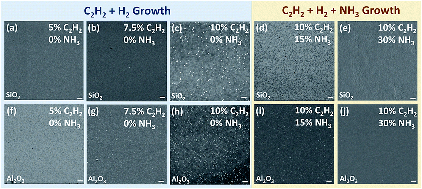 | ||
| Fig. 2 SEM images of graphene grown directly on SiO2 (a–e) and Al2O3 (f–j) at 750 °C for 3 hours by microwave PECVD using C2H2 + H2 (left column) and C2H2 + H2 + NH3 (right column), respectively. The C2H2 and NH3 concentrations are given in the images. The scale bars are 200 nm. | ||
It has been also found that further increasing of NH3 will lead to the growth of discontinuous graphene. Wei et al. studied the growth of graphene by PECVD using only NH3 and a carbon source such as C2H2, CH4 or C2H4.28 In their work, the growth temperature and the ratio of NH3 and hydrocarbon gas were systematically varied to find the optimal growth condition. High-quality graphene with low density of defects has been synthesized using this binary growth. However, only discontinuous graphene domains were produced, which will limit its applications.
Fig. 3 is the corresponding Raman spectra of the as-grown samples shown in Fig. 2. The D peak, G peak, and 2D peak, centered at around 1370, 1580, and 2700 cm−1 respectively, are the predominant features in each Raman spectrum.49 The 2D peak is a second-order two-phonon process related to a phonon near the K point in graphene, corresponds to the dispersive nature, and strongly depends on any perturbation to the electronic and/or phonon structure of graphene, therefore the 2D peak is regarded as the signature of graphene to differentiate itself from other sp2 nanocarbons.50 The G peak is caused by the stretching of the C–C bond in graphitic materials and is common in all sp2 carbon system. The D peak is caused by the disorder in the sp2 hybridized carbon atoms, and can be observed where symmetry is broken by edges or in samples with a high density of defects. In order to compare the intensities of G peaks and 2D peaks among different samples, all the D peaks in our Raman spectra were normalized.
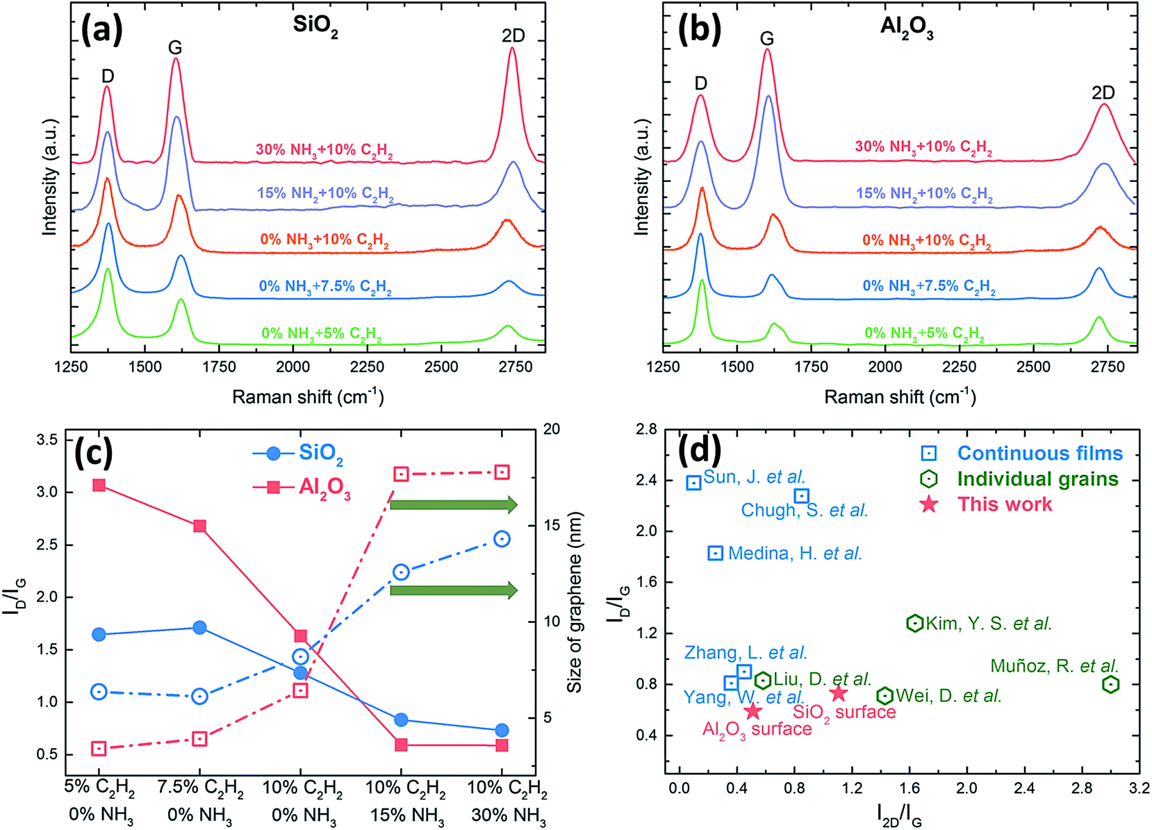 | ||
| Fig. 3 (a, b) Corresponding Raman spectra of the as-grown samples shown in Fig. 2, and (c) the intensity ratios (ID/IG, solid symbols and lines) and the sizes of graphene (open symbols and dash dot lines) of the as-grown graphene films under different conditions for three-hour synthesis at 750 °C. (d) A summary of the intensity ratios of ID/IG and I2D/IG of synthesizing graphene on insulators by PECVD method. Blue square: continuous films (Sun, J. et al.,32 Chugh, S. et al.,31 Medina, H. et al.,35 Zhang, L. et al.,38 and Yang, W. et al.36); green hexagon: individual grains (Kim, Y. S. et al.,33 Liu, D. et al.,30 Muñoz, R. et al.,27 and Wei, D. et al.28); red star: this work. | ||
The intensity ratio of D peak to G peak (ID/IG) can provide important information of the density of defects and the crystallite size of graphene.51 When evaluating these two methods of reducing 3D nano-walls, the method of introducing NH3 outweighs the method of decreasing the concentration of carbon source in reducing the density of defects and enlarging the crystallite size of graphene. Graphene grown on both SiO2 and Al2O3 substrates using C2H2/H2 plasma have a common feature that a relatively high density of defects caused by the high fraction of open edges of small crystallite sizes51 (Fig. 3a and b). By introducing NH3, ID/IG on both SiO2 and Al2O3 substrates decreases greatly by 55.6% and 80.8% respectively (Fig. 3c). As ID/IG is inversely proportional to the grain size (La) for La above 2 nm, this can be used to study the level of disorder and assess the graphene quality. It can be also used to estimate the domain sizes (or crystal sizes) using Tuinstra and Koenig relation:
| La (nm) = C(λl)(ID/IG)−1 |
The high sensitivity to the specific sp2 nanocarbons makes the 2D Raman peak very useful in distinguishing graphene with different layers.54 For metal-catalyzed CVD graphene, the intensity ratio of 2D peak to G peak (I2D/IG) ≈ 2 and a single Lorentzian 2D peak with a full width at half maximum (FWHM) of 30 cm−1 indicate monolayer graphene, the feature of 1 < I2D/IG < 2 with the 2D peak being fitted to four Lorentzian peaks is for bilayer graphene, and the feature of I2D/IG < 1 with the 2D peak being fitted to two Lorentzian peaks suggests multilayer graphene.3,4,55 However, for metal-catalyst-free CVD graphene, I2D/IG for monolayer graphene is lower (around 1.2–1.5) and the FWHM of 2D peak is broader (around 60 cm−1) due to the non-negligible D peak resulting in the breakage of the hexagonal symmetry in graphene.23,28,56 Among all the samples, the graphene grown on SiO2 substrate under 30% NH3 shows that I2D/IG ∼ 1.11 and the FWHM of 2D peak ∼57.1 cm−1, which implies monolayer graphene has been produced, and it further confirms the layer-by-layer structures observed by SEM in Fig. 2e. As for Al2O3, when increasing the NH3 concentration from 15% to 30%, I2D/IG increases from 0.39 to 0.51, which suggests that the as-grown graphene is multilayer, but its layer number reduces with the increase of NH3. Therefore, owing to the presence of NH3, and the growth mode turns from vertical graphene nano-walls to layer-by-layer films, and we can conclude that 30% NH3 is the optical condition in our system to synthesize high-quality graphene with a lower density of defects, larger crystal sizes, and fewer layers for both substrates. Fig. 3d presents the summery of the intensity ratios (ID/IG and I2D/IG) of graphene synthesized on insulators by PECVD method below 900 °C. Compared to other published works, we have achieved the growth of uniform and continuous graphene films with the lowest ID/IG using C2H2/(H2 + NH3) plasma, and Al2O3 demonstrates itself as a more competitive and suitable substrate for producing low-defect, large-area, and uniform graphene in comparison with SiO2.
To determine the electrical properties of the synthesized graphene, we fabricated back-gate graphene FETs directly using the as-grown samples without any post-transfer process. By using electron-beam lithography, oxygen plasma etching, metal deposition (5 nm Cr/50 nm Au), and lift-off technology, numbers of graphene FETs can be fabricated each time other than a single graphene domain device reported in previous work.28–30 The optical microscopy image of a typical graphene FET and its schematic structure are shown as the insets in Fig. 4a. Electrical characteristics were measured at room temperature in Keithley probe station. Fig. 4a shows the typical IDS–VDS output curves of graphene devices fabricated from the sample of graphene prepared under 30% NH3 (Fig. 2j) at various gate voltages (from −40 V to 40 V with a step of 20 V). The symmetrical linear behavior implies an ohmic contact between electrodes and graphene channel. The contact resistances are in the range of 3.8–6.6 kΩ □−1 measured by four-probe resistivity method. Fig. 4b gives the corresponding transfer curves (solid symbols) of typical five graphene FETs. For comparison, Fig. 4b also plots the transfer curve (open cycles) of a FET prepared under only H2 and C2H2. It can be seen that the FETs of graphene grown under 30% NH3 show an ambipolar transfer characteristic with the Dirac point at negative gate voltages (−20 to −30 V). On the contrary, our FETs fabricated from graphene samples grown under C2H2/H2 plasma do not show such an ambipolar transfer characteristic yet even though the gate voltage spans from −60 to +60 V. This indicates that the introduction of NH3 has an n-type doping effect on the as-grown graphene, while the graphene is normally p-type FET behavior without NH3. This is consistent with previous reports using NH3 in the growth.28,57 The average field-effect mobility was estimated to be around 16 cm2 V−1 s−1, and the mobility values were extracted from the slope of IDS–VBG based on the constant capacitance model of parallel capacitors.58
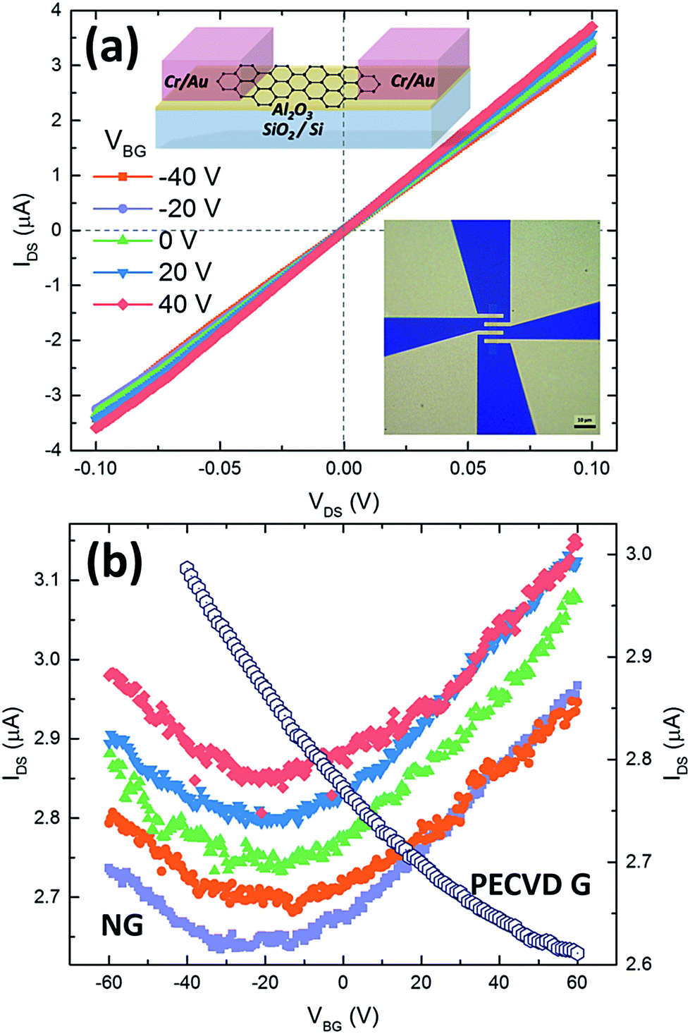 | ||
| Fig. 4 Electrical properties of graphene synthesized directly on insulators. (a) Output characteristics of graphene FETs at different gate voltages. The inset is the schematic image of the device, and the optical microscopy image of the graphene device (the scale bar is 20 μm). (b) Transfer characteristics of five graphene FETs of N-doped graphene (NG, solid symbols) and a FET device of pristine graphene (PECVD G, open symbols) produced using only H2 and C2H2 (VDS at 100 mV). | ||
The n-type doping of graphene can be also confirmed by Raman spectroscopy. Our Raman spectra in Fig. 3a and b show large downshifts of the G bands for samples prepared under different NH3 concentrations (11.8–13.5 cm−1 for SiO2 samples and 16.7–21.6 cm−1 for Al2O3 samples) compared with the sample without using NH3. This is in accordance with reported N-doped graphene,28,59 but different from ref. 60. Study has demonstrated that substitution of C atoms with graphitic N is n-type doping with a downshift in G band, while pyridinic and pyrrolic N is p-type doping with a upshift in G band.61 This means that our as-grown graphene is substitutionally doped by nitrogen atoms.
Besides the effect of NH3 concentration on the growth, the SEM images also indicate insulators have an effect on the surface morphologies of graphene. Under the same NH3 concentration and temperature, Al2O3 substrate favors a more effective nucleation stage and a faster growth stage compared with SiO2, resulting in either a higher density of 3D graphene nano-walls (Fig. 2c and h) or a better coverage on the substrate (Fig. 2e and j). The reason seems to be the smaller activation barrier of Al2O3 in the graphene growth, and such a low energy barrier ensures the dissociative adsorption of C2H2 to carbon adatom could happen at low temperature.
To further confirm that, a controlled experiment was conducted on Al2O3 substrates under the same growth condition (40 sccm C2H2, 120 sccm NH3, and 240 sccm H2) by only decreasing the growth temperature from 750 °C to 650 °C. At 750 °C, a uniform and continuous graphene film is produced (Fig. 5a), and by decreasing the growth temperature to 700 °C, graphene flakes are generated on the whole Al2O3 substrate (Fig. 5b). The Raman spectrum of sample (b) shown in Fig. 5g presents a high level of defects (ID/IG ∼ 1.8) due to the disorder and asymmetry of graphene caused by a large amount of domain boundaries and defects inside the nanographene. Although the density of defects is high, a sharp 2D peak (I2D/IG ∼ 2.27 with the FWHM of 50.3 cm−1) and the thickness of 0.7 nm measured by AFM (Fig. 5f) correspond to monolayer graphene. While at 750 °C, I2D/IG decreases to 0.51 and the 2D peak becomes broader, implying that bilayer or multilayer graphene prefers a higher temperature. By decreasing the temperature, the crystal size of graphene decreases with the maximum value of 17.8 nm obtained at 750 °C, implying that high temperature is beneficial to enlarge the size of graphene. When further decreasing the temperature into 650 °C, the whole substrate is partly covered with graphene flakes with a very high density of defects, which indicates the temperature of 650 °C is not able to provide enough energy for the growth (Fig. 5c and g). Therefore, on Al2O3 substrates, monolayer graphene growth favors a lower temperature of 700 °C, while bilayer or multilayer graphene prefers a higher temperature of 750 °C, which can promote a uniform coverage of the whole substrate, alleviate defects and disorders, and enlarge the crystal size at the same time. More importantly, the morphology of graphene grown on Al2O3 at 700 °C has similar layer-by-layer structures as that grown on SiO2 at 750 °C (Fig. 5d), while no graphene can be grown on SiO2 substrates at a temperature below 700 °C (Fig. 5e), as confirmed by Raman spectra of SiO2 in Fig. 5g. Therefore, the growth-temperature windows of these two insulators are different, which implies insulators might have different catalytic effect on the graphene growth. Part et al. carried out Density Functional Theory (DFT) calculations of activation barriers among Cu, Ni, and Al2O3 for graphene growth.62 Among these activation barriers, the supply of C adatoms governed by Ead and the enlargement of the graphene nuclei governed by Eatt determine the lowest possible growth temperature.62 From their theoretical calculations, both Ead and Eatt of Al2O3 are much lower than those of Cu while similar to the values of Ni. This indicates the graphene formation on Al2O3 could potentially be achieved at a temperature comparable to nearly the room-temperature synthesis of graphene on Ni.63 Besides Al2O3 and SiO2, other insulators including HfO2, TiO2, MnO2, quartz, and sapphire have also been used as substrates under the same condition. As their Raman spectra with low 2D peaks and high D peaks show in Fig. 5h, they are not as suitable as Al2O3 to produce monolayer and low-defect graphene at 700 °C. Therefore, the similarity and difference in the morphology of graphene on various insulators suggest that insulators might have different growth windows due to their different activation barriers, and our experiments demonstrate that Al2O3 substrates have the lowest activation barrier among others, which enables it to produce the similar structures at relatively low temperature. Further theoretical studies via DFT simulations to calculate the activation barriers of various insulators are still needed in the future, which will be beneficial to understand the potential of different insulating substrates for the low-temperature growth of graphene.
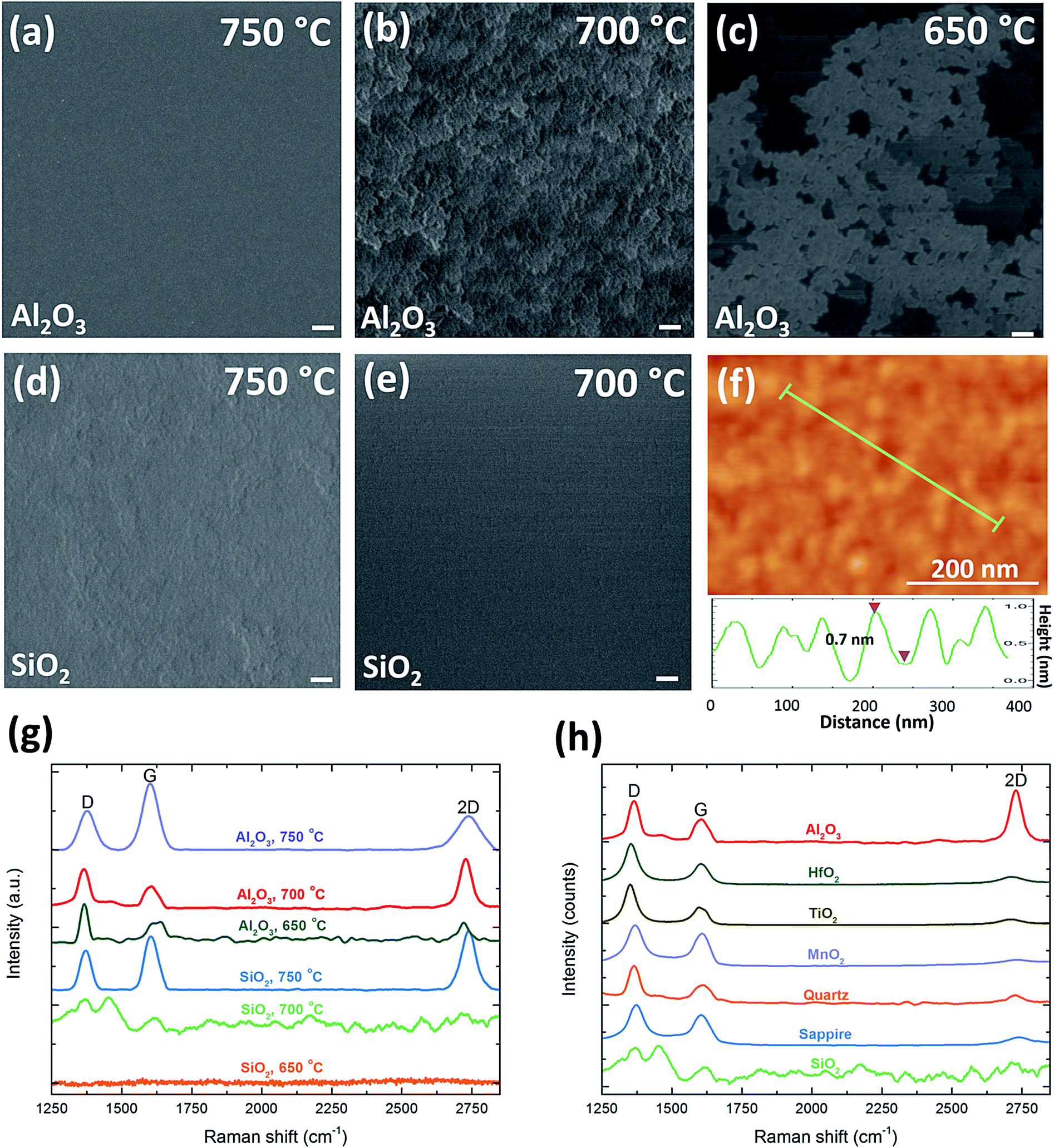 | ||
| Fig. 5 Comparison of the growth under different temperatures with 30% NH3 on Al2O3 substrates for 3 hours. SEM images of graphene grown at a temperature range of 750 °C to 650 °C on Al2O3 (a–c), and 750 °C to 700 °C on SiO2 (d, e). The scale bars are 200 nm. (f) AFM image of sample (b) and the thickness of its graphene flakes. (g) Corresponding Raman spectra of graphene samples grown on both substrates in the temperature range of 650–750 °C. (h) Raman spectra of graphene sheets grown on different insulators with 30% NH3 at 700 °C for 3 hours. | ||
Why can the growth mode of graphene be changed from 3D nano-walls to layer-to-layer films, and why is it n-type doped? Previous studies have shown that NH3 is a much stronger etchant than H2 to produce atomic hydrogen under plasma conditions, which can selectively etch away the amorphous carbon on graphene and remove defects generated at the graphene edges, thus keeping the edges atomically smooth and active during the graphene crystal growth.28,44,57 However, this could not well answer the questions. In fact, the reactions in the plasma is very complicated, which can hardly be explained by a few simple chemical reaction equations. It depends not only on the plasma type (for example, DC plasma, RF inductively coupled plasma (ICP), microwave plasma, etc.) and the plasma power, but also on the plasma gases and pressure. Mao et al. intensively investigated the plasma chemistry of different binary gas mixtures (CH4/H2, CH4/NH3, C2H2/H2 and C2H2/NH3) for the synthesis of carbon nanotubes/nanofibers by ICP enhanced CVD.64 It is found that tens of species will be formed in the plasma. Although the atomic hydrogen produced by CH4/NH3 plasma is significantly higher than that by CH4/H2 plasma at 1 torr or high pressure, the atomic hydrogen produced by C2H2/NH3 plasma is similar to that by C2H2/H2 plasma. The most fundamental thing is that long-chain hydrocarbons such as C2nH2 and C2nH6 (n up to 6) are formed and become important in the C2H2/H2 plasma. On the contrary, the formation of these long-chain hydrocarbon is less important in the C2H2/NH3 plasma. We speculate that some long-chain hydrocarbons under C2H2/H2 plasma can deposit randomly onto the substrate and develop into 3D nano-walls. By introducing higher concentration of NH3 the formation of long chain hydrocarbon is greatly suppressed, therefore the growth of 3D nano-walls is eliminated. We also believe the atomic hydrogen plays an important role in our system. This is because NH3 can be thermally decomposed to enough atomic hydrogen on the surface of substrate at 650–750 °C.65 While the thermal decomposition of H2 can be ignored due to its high stability. This explains why the quality of graphene is improved by introducing NH3. On the other hand, active HCN species can be also produced in the plasma, which can attach to the edge of graphene and form the substitutionally N-doped graphene. This results in amounts of graphitic N,57 leading to a Dirac point shift at a negative gate voltage and the downshifts of the G peaks in Raman spectra.
4. Conclusions
In summary, we have demonstrated a microwave PECVD method of synthesizing graphene on both SiO2 and Al2O3 substrates without using any metal catalysts. By introducing NH3 to suppress the formation of long-chain hydrocarbon in the plasma and to enhance the etching effect, we have obtained uniform and continuous graphene films with the lowest density of defects among all the PECVD growth of graphene. Further investigation of the effect of insulating substrates on the growth shows that the growth-temperature window and catalytic effect are different for each insulator owing to the different activation barrier. Al2O3 seems to own a lower activation barrier, which makes it a promising candidate as the substrate for the metal-catalyst-free growth of graphene at low temperature. This direct assembly of graphene on high-κ Al2O3 thin films can be flexibly incorporated into electronic and optoelectronic devices without any post-growth transfer process. More improvements are still needed in largely increasing the grain size, further reducing the growth temperature, and better controlling the number of layers. We believe our work provides an important step towards large-scale, low-cost and high-quality synthesis of graphene on arbitrary substrates.Acknowledgements
We thank EPSRC grant EP/P005152/1 and the Cambridge Commonwealth, European and International Trust for funding. S. Z. would like to acknowledge Prof. Stephan Hofmann and Dr Yuzheng Guo for helpful discussions.References
- K. S. Novoselov, A. K. Geim, S. V. Morozov, D. Jiang, Y. Zhang, S. V. Dubonos, I. V. Grigorieva and A. A. Firsov, Science, 2004, 306, 666–669 CrossRef CAS PubMed.
- K. S. Novoselov, V. I. Fal'ko, L. Colombo, P. R. Gellert, M. G. Schwab and K. Kim, Nature, 2012, 490, 192–200 CrossRef CAS PubMed.
- K. S. Kim, Y. Zhao, H. Jang, S. Y. Lee, J. M. Kim, K. S. Kim, J.-H. Ahn, P. Kim, J.-Y. Choi and B. H. Hong, Nature, 2009, 457, 706–710 CrossRef CAS PubMed.
- X. Li, W. Cai, J. An, S. Kim, J. Nah, D. Yang, R. Piner, A. Velamakanni, I. Jung, E. Tutuc, S. K. Banerjee, L. Colombo and R. S. Ruoff, Science, 2009, 324, 1312–1314 CrossRef CAS PubMed.
- Q. Yu, J. Lian, S. Siriponglert, H. Li, Y. P. Chen and S. S. Pei, Appl. Phys. Lett., 2008, 93, 113103 CrossRef.
- P. R. Kidambi, C. Ducati, B. Dlubak, D. Gardiner, R. S. Weatherup, M. B. Martin, P. Seneor, H. Coles and S. Hofmann, J. Phys. Chem. C, 2012, 116, 22492–22501 CAS.
- R. S. Weatherup, B. C. Bayer, R. Blume, C. Ducati, C. Baehtz, R. Schlögl and S. Hofmann, Nano Lett., 2011, 11, 4154–4160 CrossRef CAS PubMed.
- G. Zhong, X. Wu, L. D'Arsie, K. B. K. Teo, N. L. Rupesinghe, A. Jouvray and J. Robertson, Appl. Phys. Lett., 2016, 109, 193103 CrossRef.
- S. Bae, H. Kim, Y. Lee, X. Xu, J.-S. Park, Y. Zheng, J. Balakrishnan, T. Lei, H. R. Kim, Y. Il Song, Y.-J. Kim, K. S. Kim, B. Ozyilmaz, J.-H. Ahn, B. H. Hong and S. Iijima, Nat. Nanotechnol., 2010, 5, 574–578 CrossRef CAS PubMed.
- J. Kang, D. Shin, S. Bae and B. H. Hong, Nanoscale, 2012, 4, 5527 RSC.
- S. R. Na, J. W. Suk, L. Tao, D. Akinwande, R. S. Ruoff, R. Huang and K. M. Liechti, ACS Nano, 2015, 9, 1325–1335 CrossRef CAS PubMed.
- W. Zhang, P. Wu, Z. Li and J. Yang, J. Phys. Chem. C, 2011, 115, 17782–17787 CAS.
- S. A. Steiner, T. F. Baumann, B. C. Bayer, R. Blume, M. A. Worsley, W. J. MoberlyChan, E. L. Shaw, R. Schlögl, A. J. Hart, S. Hofmann and B. L. Wardle, J. Am. Chem. Soc., 2009, 131, 12144–12154 CrossRef CAS PubMed.
- A. Kudo, S. A. Steiner, B. C. Bayer, P. R. Kidambi, S. Hofmann, M. S. Strano and B. L. Wardle, J. Am. Chem. Soc., 2014, 136, 17808–17817 CrossRef CAS PubMed.
- M. H. Rümmeli, A. Bachmatiuk, A. Scott, F. Börrnert, J. H. Warner, V. Hoffman, J. H. Lin, G. Cuniberti and B. Büchner, ACS Nano, 2010, 4, 4206–4210 CrossRef PubMed.
- A. Scott, A. Dianat, F. Börrnert, A. Bachmatiuk, S. Zhang, J. H. Warner, E. Borowiak-Paleń, M. Knupfer, B. Büchner, G. Cuniberti and M. H. Rümmeli, Appl. Phys. Lett., 2011, 98, 73110 CrossRef.
- P.-Y. Teng, C.-C. Lu, K. Akiyama-Hasegawa, Y.-C. Lin, C.-H. Yeh, K. Suenaga and P.-W. Chiu, Nano Lett., 2012, 12, 1379–1384 CrossRef CAS PubMed.
- J. Sun, Y. Zhang and Z. Liu, ChemNanoMat, 2016, 2, 9–18 CrossRef CAS.
- D. Geng, H. Wang and G. Yu, Adv. Mater., 2015, 27, 2821–2837 CrossRef CAS PubMed.
- J. Chen, Y. Wen, Y. Guo, B. Wu, L. Huang, Y. Xue, D. Geng, D. Wang, G. Yu and Y. Liu, J. Am. Chem. Soc., 2011, 133, 17548–17551 CrossRef CAS PubMed.
- J. Chen, Y. Guo, L. Jiang, Z. Xu, L. Huang, Y. Xue, D. Geng, B. Wu, W. Hu, G. Yu and Y. Liu, Adv. Mater., 2014, 26, 1348–1353 CrossRef CAS PubMed.
- Q. Liu, Y. Gong, T. Wang, W.-L. Chan and J. Wu, Carbon, 2016, 96, 203–211 CrossRef CAS.
- M. A. Fanton, J. A. Robinson, C. Puls, Y. Liu, M. J. Hollander, B. E. Weiland, M. Labella, K. Trumbull, R. Kasarda, C. Howsare, J. Stitt and D. W. Snyder, ACS Nano, 2011, 5, 8062–8069 CrossRef CAS PubMed.
- J. Hwang, M. Kim, D. Campbell, H. A. Alsalman, J. Y. Kwak, S. Shivaraman, A. R. Woll, A. K. Singh, R. G. Hennig, S. Gorantla, M. H. Rümmeli and M. G. Spencer, ACS Nano, 2013, 7, 385–395 CrossRef CAS PubMed.
- J. Kim, M. Ishihara, Y. Koga, K. Tsugawa, M. Hasegawa and S. Iijima, Appl. Phys. Lett., 2011, 98, 91502 CrossRef.
- X. Chen, B. Wu and Y. Liu, Chem. Soc. Rev., 2016, 45, 2057–2074 RSC.
- R. Muñoz, C. Munuera, J. I. Martínez, J. Azpeitia, C. Gómez-Aleixandre and M. García-Hernández, 2D Mater., 2017, 4, 15009 CrossRef PubMed.
- D. Wei, L. Peng, M. Li, H. Mao, T. Niu, C. Han, C. Wei, W. Chen, A. Thye and S. Wee, ACS Nano, 2015, 1, 1–15 Search PubMed.
- D. Wei, Y. Lu, C. Han, T. Niu, W. Chen and A. T. S. Wee, Angew. Chem., Int. Ed., 2013, 52, 14121–14126 CrossRef CAS PubMed.
- D. Liu, W. Yang, L. Zhang, J. Zhang, J. Meng, R. Yang, G. Zhang and D. Shi, Carbon, 2014, 72, 387–392 CrossRef CAS.
- S. Chugh, R. Mehta, N. Lu, F. D. Dios, M. J. Kim and Z. Chen, Carbon, 2015, 93, 393–399 CrossRef CAS.
- J. Sun, M. E. Schmidt, M. Muruganathan, H. M. H. Chong and H. Mizuta, Nanoscale, 2016, 8, 6659–6665 RSC.
- Y. S. Kim, K. Joo, S.-K. Jerng, J. H. Lee, E. Yoon and S.-H. Chun, Nanoscale, 2014, 6, 10100–10105 RSC.
- C. Yang, H. Bi, D. Wan, F. Huang, X. Xie and M. Jiang, J. Mater. Chem. A, 2013, 770–775 CAS.
- H. Medina, Y.-C. Lin, C. Jin, C.-C. Lu, C.-H. Yeh, K.-P. Huang, K. Suenaga, J. Robertson and P.-W. Chiu, Adv. Funct. Mater., 2012, 22, 2123–2128 CrossRef CAS.
- W. Yang, C. He, L. Zhang, Y. Wang, Z. Shi, M. Cheng, G. Xie, D. Wang, R. Yang, D. Shi and G. Zhang, Small, 2012, 8, 1429–1435 CrossRef CAS PubMed.
- A. Malesevic, R. Vitchev, K. Schouteden, A. Volodin, L. Zhang, G. Van Tendeloo, A. Vanhulsel and C. Van Haesendonck, Nanotechnology, 2008, 19, 305604 CrossRef PubMed.
- L. Zhang, Z. Shi, Y. Wang, R. Yang, D. Shi and G. Zhang, Nano Res., 2010, 4, 315–321 CrossRef.
- J. Sun, Y. Chen, X. Cai, B. Ma, Z. Chen, M. K. Priydarshi, K. Chen and T. Gao, Nano Res., 2015, 8, 3496–3504 CrossRef CAS.
- A. T. H. Chuang, J. Robertson, B. O. Boskovic and K. K. K. Koziol, Appl. Phys. Lett., 2007, 90, 123107 CrossRef.
- Y. Zhang, V. W. Brar, C. Girit, A. Zettl and M. F. Crommie, Nat. Phys., 2009, 5, 722–726 CrossRef CAS.
- S. Kim, J. Nah, I. Jo, D. Shahrjerdi, L. Colombo, Z. Yao, E. Tutuc and S. K. Banerjee, Appl. Phys. Lett., 2009, 94, 62107 CrossRef.
- B. Dlubak, P. R. Kidambi, R. S. Weatherup, S. Hofmann and J. Robertson, Appl. Phys. Lett., 2012, 100(17), 173113 CrossRef.
- L. Zhang, M. Ni, D. Liu, D. Shi and G. Zhang, J. Phys. Chem. C, 2012, 116, 26929–26931 CAS.
- L. Xie, L. Jiao and H. Dai, J. Am. Chem. Soc., 2010, 132, 14751–14753 CrossRef CAS PubMed.
- M. S. Bell, R. G. Lacerda, K. B. K. Teo, N. L. Rupesinghe, G. A. J. Amaratunga, W. I. Milne and M. Chhowalla, Appl. Phys. Lett., 2004, 85, 1137–1139 CrossRef CAS.
- M. S. Bell, K. B. K. Teo, R. G. Lacerda, W. I. Milne, D. B. Hash and M. Meyyappan, Pure Appl. Chem., 2006, 78, 1117–1125 CrossRef CAS.
- D. H. Lee, W. J. Lee and S. O. Kim, Nano Lett., 2009, 9, 1427–1432 CrossRef CAS PubMed.
- A. C. Ferrari, J. C. Meyer, V. Scardaci, C. Casiraghi, M. Lazzeri, F. Mauri, S. Piscanec, D. Jiang, K. S. Novoselov, S. Roth and a. K. Geim, Phys. Rev. Lett., 2006, 97, 187401 CrossRef CAS PubMed.
- M. S. Dresselhaus, A. Jorio, M. Hofmann, G. Dresselhaus and R. Saito, Nano Lett., 2010, 10, 751–758 CrossRef CAS PubMed.
- A. C. Ferrari, Solid State Commun., 2007, 143, 47–57 CrossRef CAS.
- A. C. Ferrari and J. Robertson, Phys. Rev. B: Condens. Matter Mater. Phys., 2000, 61, 14095–14107 CrossRef CAS.
- L. G. Caņado, K. Takai, T. Enoki, M. Endo, Y. a. Kim, H. Mizusaki, A. Jorio, L. N. Coelho, R. Magalhães-Paniago and M. a. Pimenta, Appl. Phys. Lett., 2006, 88, 12–14 Search PubMed.
- L. M. Malard, M. a. Pimenta, G. Dresselhaus and M. S. Dresselhaus, Phys. Rep., 2009, 473, 51–87 CrossRef CAS.
- D. Graf, F. Molitor, K. Ensslin, C. Stampfer, A. Jungen, C. Hierold and L. Wirtz, Nano Lett., 2007, 7, 238–242 CrossRef CAS PubMed.
- S. Xu, B. Man, S. Jiang, W. Yue, C. Yang, M. Liu, C. Chen and C. Zhang, Nanotechnology, 2014, 25, 165702 CrossRef PubMed.
- D. Wei, Y. Liu, Y. Wang, H. Zhang, L. Huang and G. Yu, Nano Lett., 2009, 9, 1752–1758 CrossRef CAS PubMed.
- D. K. Schroder, Semiconductor Material and Device Characterization, John Wiley & Sons, 2006 Search PubMed.
- L. Zhao, R. He, K. T. Rim, T. Schiros, K. S. Kim, H. Zhou, C. Gutierrez, S. P. Chockalingam, C. J. Arguello, L. Palova, D. Nordlund, M. S. Hybertsen, D. R. Reichman, T. F. Heinz, P. Kim, A. Pinczuk, G. W. Flynn and A. N. Pasupathy, Science, 2011, 333, 999–1003 CrossRef CAS PubMed.
- S. M. Shinde, E. Kano, G. Kalita, M. Takeguchi, A. Hashimoto and M. Tanemura, Carbon, 2016, 96, 448–453 CrossRef CAS.
- D. Deng, X. Pan, L. Yu, Y. Cui, Y. Jiang, J. Qi, W. X. Li, Q. Fu, X. Ma, Q. Xue, G. Sun and X. Bao, Chem. Mater., 2011, 23, 1188–1193 CrossRef CAS.
- J. Park, J. Lee, J.-H. Choi, D. K. Hwang and Y.-W. Song, Sci. Rep., 2015, 5, 11839 CrossRef PubMed.
- J. Kwak, J. H. Chu, J.-K. Choi, S.-D. Park, H. Go, S. Y. Kim, K. Park, S.-D. Kim, Y.-W. Kim, E. Yoon, S. Kodambaka and S.-Y. Kwon, Nat. Commun., 2012, 3, 645 CrossRef PubMed.
- M. Mao and A. Bogaerts, J. Phys. D: Appl. Phys., 2010, 43, 205201 CrossRef.
- A. H. White and W. M. Melville, J. Am. Chem. Soc., 1904, 27, 373–386 CrossRef.
| This journal is © The Royal Society of Chemistry 2017 |