
 Open Access Article
 This Open Access Article is licensed under a
 Creative Commons Attribution 3.0 Unported Licence
Broadband quarter-wave plate based on dielectric-embedded plasmonic metasurface
Edgar O. Owiti abce,
Hanning Yangabc,
Calvine F. Omindee and
Xiudong Sun*abcd
abce,
Hanning Yangabc,
Calvine F. Omindee and
Xiudong Sun*abcd
aInstitute of Modern Optics, Department of Physics, Harbin Institute of Technology, Harbin 150001, China. E-mail: eowiti@hit.edu.cn; xdsun@hit.edu.cn
bKey Laboratory of Micro-Nano Optoelectronic Information System of Ministry of Industry and Information Technology, Harbin 150001, China
cKey Laboratory of Micro-Optics and Photonics Technology of Heilongjiang Province, Harbin 150001, China
dCollaborative Innovation Center of Extreme Optics, Shanxi University, Taiyuan, Shanxi 030006, China
eDepartment of Physics, Jomo Kenyatta University of Agriculture and Technology, P.O. Box 62000-00200, Nairobi, Kenya
First published on 31st July 2017
Abstract
High transmission plasmonic and all-dielectric metasurface wave plates have been reported in recent studies. However, narrow bandwidth and low polarization conversion need to be addressed to attain even better operation requirements. In this work, we numerically demonstrate the concept of an ultrathin single layer plasmonic metasurface embedded with dielectric resonators. Our design is based on the transmission line theory and surface plasmon excitation to realize a quarter-wave plate with controllable birefringence. The controllability is achieved through manipulating relative permittivity of a non-dispersive dielectric material-embedded in a perforated silver film, and the surface dimensions of silver. We have also achieved higher degrees of linear-to-circular and circular-to-linear polarization conversions at broadband wavelengths in the near infrared compared with other conventional plasmonic metasurfaces. Moreover, the functioning of the wave plate is demonstrated on a compact and ultrathin metasurface showing great potential of integration into photonic sensors.
1 Introduction
A birefringent metasurface is a two dimensional structure with an ability of independently controlling the phase, amplitude, and polarization of an incident polarized light. The concept of metasurfaces has opened up many new opportunities for the efficient manipulation of light and design of unique devices like the quarter-wave plate (QWP). Properties such as amplitude and phase control,1 beam splitting,2,3 and beam focusing4 have all been realized using metasurfaces. Naturally occurring crystals such as quartz and calcite exhibit weak birefringence in the infrared due to their small refractive indices. To realize a desired phase retardation and polarization state, thickness-dependent birefringent crystals have to be employed.5 Metamaterials and metasurfaces are being studied to realize and develop ultrathin wave plate structures that can be integrated into nanophotonic devices. However, the progress of metasurface wave plates is hindered by the following challenges: low conversion efficiency, fabrication complexity, bulk thicknesses, and narrow bandwidth.6–8 By placing two layers of orthogonal slits in parallel to each other, an induced 90 degree polarization conversion and enhanced transmission have been demonstrated.9 Huang et al.,9 showed that despite the bulk thickness of the grating-like dual surface, a tunable wave plate based on slits dimensions was attainable within the visible spectrum. Similarly, a dual layer wave plate with tunable birefringence based on the spacing distance between the layers have been shown.10 Other plasmonic structures based on L-shaped antennas,11,12 T-shaped slits and antennas,13,14 crossed-shaped slits,15 metal–insulator–metal designs,16 among others, have also been designed and demonstrated performing polarization conversions on ultrathin dimensions. However, due to dispersion properties and ohmic losses in plasmonic metals, such structures have been reported exhibiting wave plate properties at narrow band frequencies limited to 3–5% of center frequency.17–19All-dielectric metasurfaces based on silicon are an alternative to reduce ohmic losses in plasmonic metasurfaces.20–22 Recently, Chong et al. demonstrated a transmission mode metasurface using thin silicon nanoantennas; simultaneous electric and magnetic dipole resonances in silicon were excited to mitigate back reflection, create an impedance matching with the incident light, and induce polarization.23 Efficient wavefront manipulation in transmission such as Gaussian to vortex beams, have also been reported using silicon dielectrics.23,24 In addition, the merits of a 2D graphene material structured with gold and a silicon dioxide spacer have been explored where polarization conversion ratios (PCR) greater than some natural birefringent crystals such as calcite were reported.25 Dual layer metamaterial consisting of a semiconductor, a fused silica spacer, and split ring resonators has also been shown with considerable birefringence and compactness.26 However, such structures are bulky and have a limitation to be integrated into nanophotonic sensors. Purely plasmonic metasurfaces have strong field localization, enhancement, and extra ordinary transmission due to interaction of light with the surface plasmon polaritons (SPP).27,28 They have superior optical response across a wider region of the electromagnetic (EM) spectrum. Their main drawback is the presence of ohmic losses which reduce efficiency of polarization conversion.
We present a hybrid plasmonic metasurface with reduced absorptive losses exhibiting broad bandwidth QWP performance operating in transmission mode. We exploit the merits of dielectric materials acting as gain materials embedded in a low loss plasmonic silver metal. A single layer wave plate metasurface that functions as a lumped circuit element with nanoinductors and nanocapacitors is designed. All numerical simulations were done using finite element method, COMSOL Multiphysics. By varying the dielectric constant of the embedded dielectric materials, a dipole moment is created and a phase retardation is obtained. Birefringence tunability is then achieved through varying dielectric constants and the dimensions of the structure.
2 Structure design, numerical simulations, results and discussions
Fig. 1 shows a schematic illustration of the designed structure operating as a QWP. The unit cell shows the dimensions of the structure, composed of two pairs of orthogonal rectangular slits filled with a dielectric material. The longer pair is oriented along the x-axis with length L1 = 200 nm, and the shorter pair oriented along the y-axis with length L2 = 175 nm. The structure has a thickness h = 120 nm, a common slit's width W = 50 nm, and lateral spacings t = 30 nm. All dimensions are sub-wavelength with respect to the near infrared wavelengths from 600 nm to 1500 nm. The relative permittivity of silver was modeled using the Drude's equation, εAg(ω) = ε∞ − ωp2/(ω2 + iγ2), fitting the experimental standard data of Johnson and Christy,29 where ε∞ = 5 is the infinite-frequency limit of the relative permittivity, ωp = 1.7601 × 10¹⁶ rad s−1 is the plasma frequency, and γ = 3.0841 × 10¹⁴ rad s−1 is the damping factor. Perfectly matched layers absorbing boundaries were placed on the exit end of the unit cell to prevent non-physical reflections of outgoing waves and periodic boundaries implemented along the x and y planes.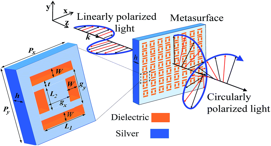 | ||
| Fig. 1 Schematic illustration showing single layer QWP operating in LTC conversion mode, and left, metasurface unit cell dimensions; W = 50 nm, L1 = 200 nm, L2 = 175 nm, t = 30 nm, gx = L1 − 2W, and gy = L2 + 2t. | ||
The slits dimensions were carefully optimized considering both the phase and momentum matching conditions.30 Naturally, a mismatch in phase exists between the parallel surface component of the free-space wave vector ![[k with combining right harpoon above (vector)]](https://www.rsc.org/images/entities/i_char_006b_20d1.gif) ∥ and the SPP wave vector
∥ and the SPP wave vector ![[K with combining right harpoon above (vector)]](https://www.rsc.org/images/entities/i_char_004b_20d1.gif) SPP. The nature of the periodic structure allows SPPs to propagate in orthogonal directions determined by the periodicities. The periodicities are thus used to obtain an optimum transmission region and meet the phase matching condition,
SPP. The nature of the periodic structure allows SPPs to propagate in orthogonal directions determined by the periodicities. The periodicities are thus used to obtain an optimum transmission region and meet the phase matching condition, 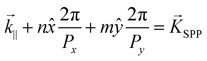 , where ∥ = o
![[thin space (1/6-em)]](https://www.rsc.org/images/entities/char_2009.gif) sinθ, θ is angle of incidence, n and m are integers representing coupling diffraction orders or Bloch modes, and o is free-space wave vector for the incident light. The structure was normally illuminated (θ = 0°) from the bottom of the substrate by linearly polarized plane waves; Ei =
sinθ, θ is angle of incidence, n and m are integers representing coupling diffraction orders or Bloch modes, and o is free-space wave vector for the incident light. The structure was normally illuminated (θ = 0°) from the bottom of the substrate by linearly polarized plane waves; Ei = ![[x with combining circumflex]](https://www.rsc.org/images/entities/i_char_0078_0302.gif) Eoxexp(jkoz) and Ei = ŷEoyexp(jkoz) propagating in the +z direction. We used Jones vector excitations
Eoxexp(jkoz) and Ei = ŷEoyexp(jkoz) propagating in the +z direction. We used Jones vector excitations  ,
,  , and
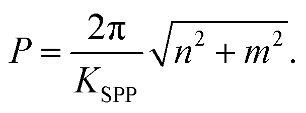
, and 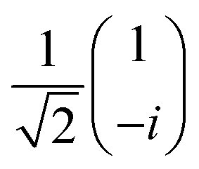 , for linearly polarized light (LP), right-handed circularly polarized light (RCP), and left-handed circularly polarized light (LCP), respectively, where α is the angle of polarization used to control the amplitude of the incident light. The interface between the metal and the semi-infinite silicon dioxide (SiO2) substrate facilitates SPP-to-incident light coupling. At normal incidence (θ = 0°) both the phase matching condition and the momentum conservation,
 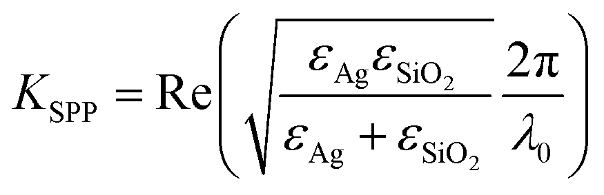 , reduce to an analytical square periodicity equation
 | (1) |
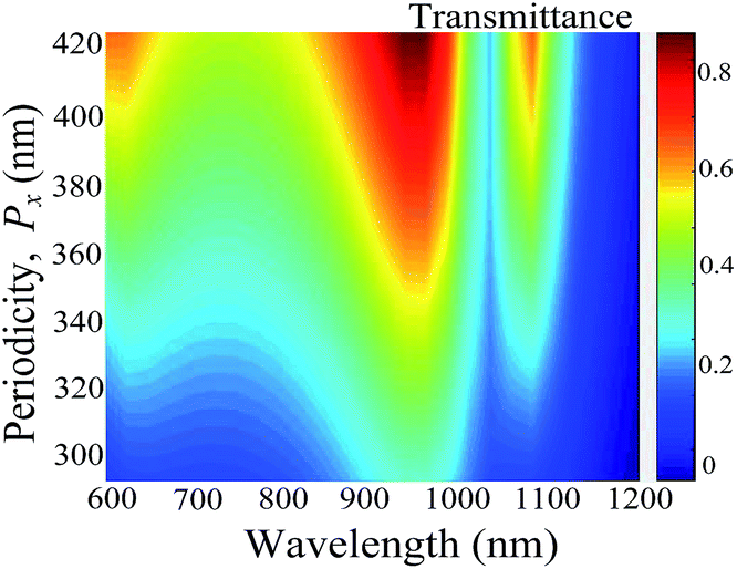 | ||
| Fig. 2 Transmittance spectrum as a function of periodicity Px at fixed values of Py = 420 nm, L1 = 200 nm, and L2 = 175 nm. | ||
Transmission properties of the structure were studied by first setting the model with port boundary conditions along the +z and −z directions and then using absolute S-parameters to calculate the transmittance, reflectance and absorption spectra as shown in Fig. 3(a). The obtained wavelength bandwidth of interest describes the nanocircuit's optimum region where maximum displacement current is experienced. As the current circulates the surface, the plasmonic metal (Re[εAg] < 0) functions as a nanoinductor while the dielectric fillings in the slits, Re[εr] > 0, function as nanocapacitors. Therefore, lumped circuit elements were optimized to manipulate polarization conversion by sweeping through several values of different parameters. In this case, the dimensions of the metal and the relative permittivity of the dielectric filling have been demonstrated to manipulate the phase retardation Δϕ. Here, Δϕ = arg(Etx/Ety), where Etx and Ety are complex electric fields in the transmission field. Birefringence of the metasurface is defined using Δϕ, i.e., the difference between the x and y phase components, ϕxx = arg(Etx) and ϕyy = arg(Ety). The birefringence of the desired wave plate is one that induces a phase difference of ±90° for a LP excitation, and ±180° or 0° for a circularly polarized light (CP) excitation.
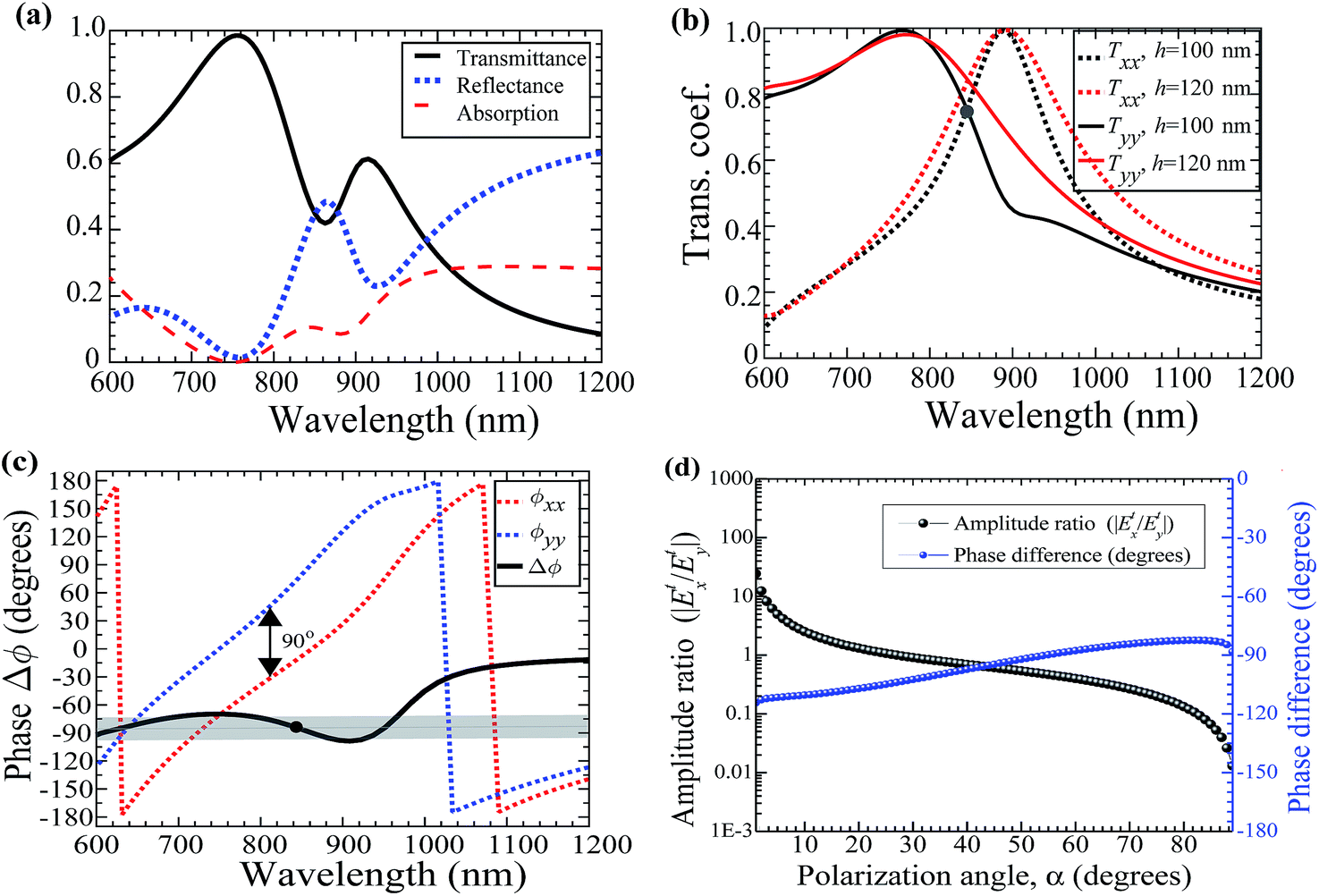 | ||
| Fig. 3 LTC: (a) transmission, reflection, and absorption spectra calculated at periodicities Px = 370 nm and Py = 420 nm. (b) Transmission coefficients as a function of thickness h, and (c) corresponding transmission phase components and phase difference Δϕ. The inserted black circles in (b) and (c) indicate that the coefficients are the same and Δϕ = −90°. (d) Transmission amplitude ratio and phase difference as a function of polarization angle. | ||
The wavelength region (λ = 600 nm to λ = 950 nm) corresponds to the area of maximum coupling between the SPPs and the incident light and also where there is acceptable transmittance. Meanwhile, in Fig. 3(b), the thickness of silver layer, h, shows negligible effect on the transmission coefficients. We have used, h = 120 nm, throughout the simulations except in cases where it was a variable. At λ = 850 nm, considered as the design wavelength, the co-polarization terms show an intersection point where both x- and y-amplitude components are equal, Txx = Tyy, where Txx = |Etx| and Tyy = |Ety|. The corresponding phase angles are shown in Fig. 3(c) for α = 60°, L1 = 200 nm, L2 = 175 nm, and optimum periodicities. It can be seen that an ideal QWP condition occurs only at the design wavelength where both accurate phase and amplitude requirements are met. However, when Δϕ is within ±90° ± 5°, and the ratio of transmission amplitudes |Etx/Ety| is within 0.8 and 1.2, QWP performance is still acceptable as illustrated in Fig. 3(c) (grey band), and Fig. 3(d), respectively. In Fig. 3(d), the structure shows a higher degree of insensitivity to polarization angles swept between [1°, 89°] at λ = 850 nm.
In our analysis, when the wave plate operates at a wavelength within or slightly away from the SPP coupling region, a tunable phase shift occurs between the components in the transmission field.14 Modifying the dimensions, Li (i = 1, 2) and Pi (i = x, y), contribute to the phase difference between the SPP modes as well as to the orthogonal components of the transmitted electric fields; ϕSPP,x − ϕSPP,y = ±90°, where ϕSPP,x,y are the relative phases of the two SPP modes. Fig. 4(a) displays electric field of the SPP mode (1, 0) when L1 = 200 nm and L2 = 175 nm in the x–y plane (z = 0). An electric field enhancement characterized by SPP mode around the slit filled with air is shown, attributed to the antisymmetric current distributions. Dielectric fillings inside the slits, and the potential across the resonators also contribute highly to the tuning of phase angles as hereby discussed. In the region of interest, silver has finite conductivity σ, therefore, the conduction current is suppressed from the surface while the tangential electric displacement current dominates, i.e., Jd = −iωεrE, where εr is the dielectric constant of the slit embedding material. The displacement current impinges on the structure and activates the surface as it circulates through the plasmonic metal and the dielectric. In this process, a dipole moment is induced inside the dielectric and creates a spatial potential and localized electric field E(r, θs) = ∇Φ on the surface as illustrated in Fig. 4(b). The simulated local electric field distribution Eref/Eo under x- and y-LP lights are shown in Fig. 4(c) and (d), respectively, where Eref is the local electric field within the dipole and Eo = 1 V m−1. The electric fields align the dipoles and create a potential across the dielectrics. Regardless of the state of polarization, the orthogonal dielectric inclusions are independently polarized. In general, the dependence of the resonator dimensions, Li (i = 1, 2), on the potential have been demonstrated following the relationship Φ ∝ (ELi3/r2)cosθs.32 The wave plate operation can thus be inferred from the relation ΔΦ ∝ Δϕ, where ΔΦ is the potential difference across orthogonal resonators and Δϕ is phase difference between the x- and y-components of the transmitted light. As shown in Fig. 5(a) and (b), a reduction in the dimension L2 and an increment in the relative permittivity εr of the dielectric filling, causes a vertical shift in Δϕ and a horizontal red-shift in the birefringence bandwidth, respectively. This behaviour is due to a change in the potential difference across the resonators that develops due to combined impedances on the surface. Moreover, the region within the wavelength bandwidth shows a larger phase change compared to other regions. In this region, the displacement current Jd is at maximum and the nanocapacitance has its maximum electric energy within the dielectric. Fig. 5(c) shows the results of phase retardation against the wavelength for a CP incident light. A wavelength bandwidth, Δλ = 250 nm, for which Δϕ ≈ 0° (grey band) is observed. Similar to the variations of L1 and L2 in Fig. 5(a), the thickness h when increased produces a vertical downward shift on Δϕ around the wavelength bandwidth. In the lumped circuit configuration, the dipole moments and the impedances are manipulated by selecting and varying different surface dimensions and the dielectric constant of the embedded material, causing the area around resonance to show a Δϕ dip over a broad range. The shift in phase is observed for both circular-to-linear (CTL) and linear-to-circular (LTC) polarization conversions as shown in Fig. 5(c) and (d), respectively.
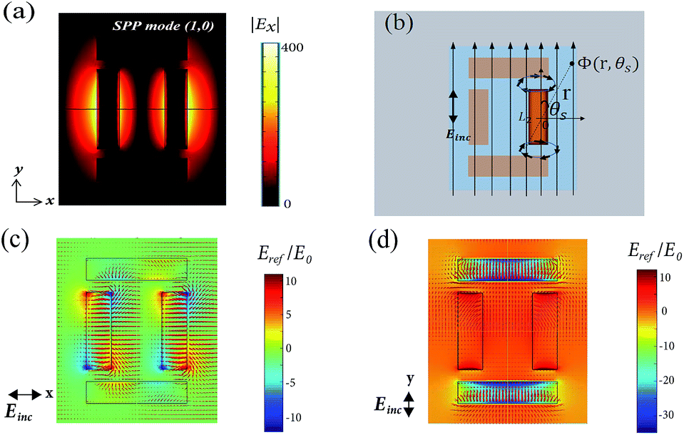 | ||
| Fig. 4 (a) SPP mode (1, 0) excitation. (b) Dipole mode illustration. Electric field distribution on the surface of the structure calculated at λ = 850 nm for, (c) x-polarization, and (d) y-polarization. | ||
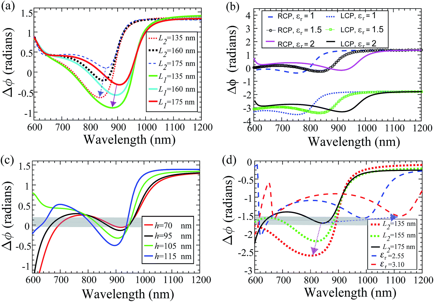 | ||
| Fig. 5 Phase retardation for LTC (a–c), and CTL (d) conversions at fixed values of α = 60°, Px = 370 nm, and Py = 420 nm. (a) Both L1 and L2 are varied while εr values are fixed at 2.21 and 1.0, respectively. L1 = 200 nm when L2 is varied, and L2 = 175 nm when L1 is varied. (b) εr varied but L1 = 200 nm and L2 = 175 nm. (c) Thickness, h, varied and other dimensions fixed as shown above. (d) L2 and εr varied at L1 = 200 nm. | ||
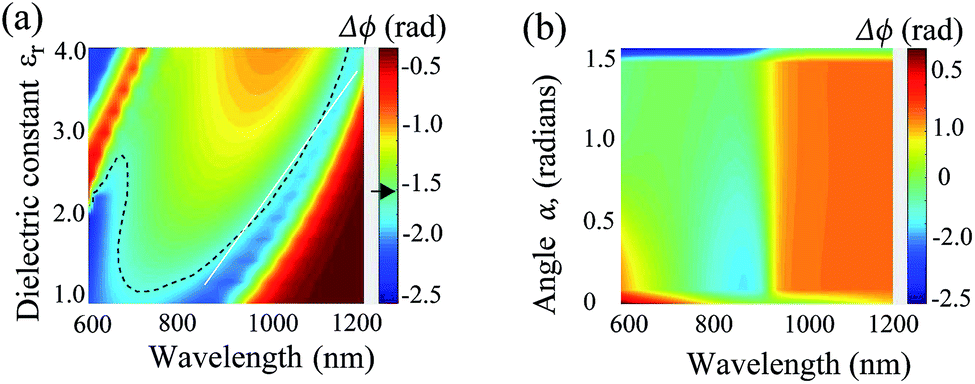
In Fig. 6(a), a phase map variation of the dielectric constant and wavelength is shown. The dotted black line region indicates where 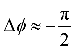 can be accurately obtained with respect to the wavelength for a LP light excitation. The dipole moment per unit volume Pν = (εr − 1)/ε0E is enhanced as long as εr is large enough, which translates to a higher polarizability inside the resonators; an almost linearly varying QWP phase condition between λ = 830 nm and 1000 nm (white line in Fig. 6(a)) can be easily noted. Similarly, the angle α defines the magnitude of the x- and y-components of the incident field. For small fields, the magnitude of dipole moment per unit volume is proportional to the electric field strength. As shown in Fig. 6(b), when the angle of polarization is ≈60° for CP input, QWP condition is satisfied between λ = 600 nm and 900 nm. Both phase and amplitude QWP conditions are met with
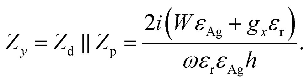
  . Since the metal is functioning as a nanoinductor and the embedded dielectric material with relative permittivity Re[εr] > 0 as a nanocapacitor, together forming lumped circuit elements, we consider a quasi-static approximation based on the subwavelength dimensions of the structure and analyse the current–impedance interaction based on the transmission line theory.33 Two types of circuit networks develop on the surface as a result of this interaction: a parallel and a perpendicular network, depending on the resonator's orientation and the polarization state of incident light (inset of Fig. 7). If the x-oriented dielectric resonators in Fig. 1(a) are considered perpendicular to y-polarization, the impedance from the plasmonic metal and the dielectric are functions of the relative permittivity and the dimensions given as
 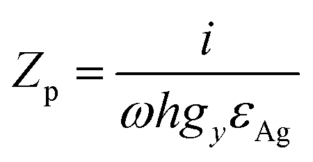 and
and 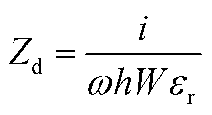 per unit length, respectively, giving an effective network impedance
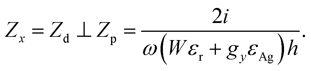 | (2) |
 | ||
| Fig. 6 Dispersion of phase retardation ΔΦ for; (a) dielectric constant εr variation with wavelength for LTC conversion at fixed L1 = 200 nm and L2 = 175 nm, and (b) CTL conversion at fixed εr = 2.25 and α varied. | ||
 | ||
| Fig. 7 Normalized transmittance comparison between the circuit model and full wave simulation at the design wavelength. Inset; lumped circuit model configuration for different slit orientations. | ||
When the electric field is parallel to the y-oriented resonators the impedance equations 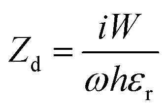 and
and 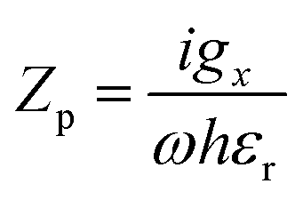 are used, giving an effective impedance
 | (3) |
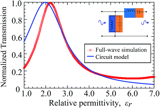
Consequently, a potential Φi = JimpZi, (i = x, y) builds up across the lumped elements, where Jimp is an impressed current. Orthogonal orientation of the resonators enhance potential difference ΔΦ for any excitation state of incident light. This is due to the difference in the dipole moments and the SPP modes excited by components of the electric field. In addition, since eqn (2) and (3) are functions of dimensions and the relative permittivity of inclusions, any variation in the relative permittivity and/or the dimensions tunes the birefringence to QWP condition. To validate the metasurface as a composition of lumped circuit elements, eqn (2) and (3) were used to calculate transmittance Ti = |(Zi/(Zi + [η0/2(gi + 2W))])|2, (i = x, y) as a function of surface dimension and compared the calculated transmittance with full wave simulation transmittance. Here, η0 = 377 Ω is the free-space surface impedance. A nearly coinciding transmittance peak around εr = 2.2, calculated at λ = 850 nm, was observed as shown in Fig. 7. The dielectric resonators and the plasmonic metal can then be verified to function as lumped circuit elements in the near infrared. We then quantified the degree of cross polarization conversion using the polarization conversion ratio (PCR) defined as PCR = Txy2/(Txy2 + Tyy2), where Txy and Tyy are cross-polarized and co-polarized transmission coefficient terms, respectively. A 90% polarization conversion ratio in the range λ = 600 nm to λ = 750 nm was obtained for a dielectric material εr = 2.55 as shown in Fig. 8(a). For a smaller dielectric constant εr = 1.0 (for air) a reduced PCR range was observed due to the weak coupling effect. It is worth noting that the high PCR value confirms the energy conversion from one state of LP light to the other.
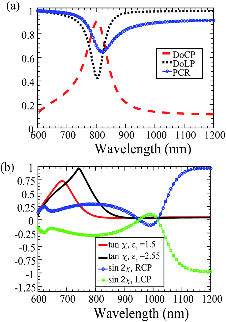 | ||
| Fig. 8 Figures of merit. (a) Calculated DoLP, DoCP and PCR, and (b) ellipticity calculations in variation with εr and RCP and LCP excitation. | ||
To analyze polarization performance through the wave plate, Stokes parameters S1, S2, and S3 were calculated from the transmission coefficients and used to determine important figures of merit such as the degree of linear polarization (DoLP), degree of circular polarization (DoCP), and the ellipticity η. Fig. 8(a) and (b) show the figures of merit used to analyze the performance of the structure. DoLP was obtained as 0.98 in the range between λ = 900 nm and 1200 nm. In this regard, the linear polarization conversion from an incident CP light translates into a broadband QWP regardless of the direction of the transmitted light. Fig. 5(c) and (d) show the bandwidth over which the DoLP is nearly unity. We calculated the DoCP of the transmitted light within the bandwidth where DoLP ≈ 1. As expected, the DoCP was very small (≈0.11), confirming maximum linear polarization. For a LP light, the ellipticity angle 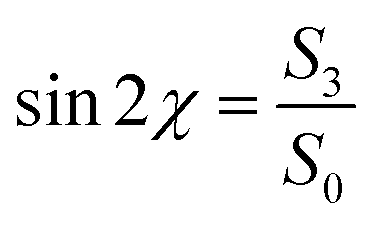 satisfies the required condition, sin2χ ≈ 0, and for a CP light the ellipticity η = tanχ is approximately unity at λ = 750 nm and εr = 2.55. The QWP bandwidth can thus be quantified as the ratio of wavelength bandwidth Δλqw, where DoLP or DoCP > 90%, to the wavelength bandwidth Δλ, where the phase retardation is ±90° and the amplitude ratio is approximately unity.34 In this case, the ratio is about 25% of central wavelength.
By embedding a dielectric material in the metal slits, both electric and magnetic Mie resonances, originating from excitation of a particular electromagnetic mode within the resonator, are supported.23,35 Besides polarization conversion, the efficiency of the structure is enhanced through impedance matching effect coming from destructive interference between the overlapping back scattering electric and magnetic modes, and the incident light. High transmission above 40% and up to 100%, and low reflection are achieved within polarization conversion bandwidth (Fig. 3(a)). As shown in the results, a precise combination of relative permittivity (εr > 0) of the dielectric material and (Re[εAg] < 0) of silver metal, yields a desired QWP phase retardation between the transmitted x- and y-polarized lights. The dual pair rectangular orthogonal slits behaves like a meander line polarizer:36 to the s-polarized signal, the vertically filled rectangular pair and the plasmonic areas act like shunted inductors over an equivalent transmission line while the p-polarized signal is capacitively affected. Therefore, an incident light polarized in the range 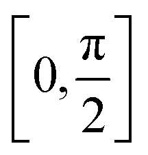 is decomposed into vertical and horizontal components where the s-polarized is delayed and p-polarized light advanced. After transmission of the electric field, the two components recombine with phase difference of either ±π/2, forming a CP light or ±π (or 0 rad) forming a LP light (Fig. 1(a)). The applied electric field on embedded dielectric material affects the orientation of the dipoles, it causes a polarization effect thus changing both nanocapacitance and effective impedance of the metasurface. A reduction in effective permittivity increases surface capacitance. We reiterate that the potential difference between the orthogonal resonators is the main agent of the phase change. Each resonator can be looked at as a pixel because light is confined inside the dielectric fillings regardless of the presence of a dielectric. When the slit is filled with air (εr = 1), the resonator is weakly coupled and only the dimensions can be used to tune birefringence. Thus, for this structure the transmission efficiency is affected by the geometrical parameters and the embedded dielectric material in the plasmonic metal.
3 Conclusion
In summary, an ultrathin QWP metasurface working in the near infrared has been numerically designed and demonstrated. Birefringence of the wave plate is controllable through manipulating dielectric fillings in the slits and metal dimensions that control the SPP modes. A broadband QWP wavelength of 250 nm translating to ≈25% of the central wavelength has been obtained. In addition, the designed structure shows high degrees of PCR (>90%), DoLP (>90%), and DoCP (>85%) despite the presence of the metal. Finally, the range of relative permittivity values used to control birefringence was carefully selected to match what is physically available, in particular, polydimethylsiloxane (PDMS) has acceptable optical response in the near infrared and is a suitable material for the device fabrication. A broader bandwidth and an enhanced tunability can be obtained by filling the x and y oriented slits with different dielectric materials. In such a structure, orthogonal SPP modes can be detuned based on both the dimensions and the different refractive indices. In future, we propose an experimental realization using optical materials such as titanium dioxide (TiO2) and PDMS. Also, a different design with dimensions that are scaled downwards can be implemented to achieve a similar QWP bandwidth in lower wavelengths less than 600 nm.Acknowledgements
This work was supported by the National Key Basic Research Program of China (No. 2013CB328702) and the National Natural Science Foundation of China (NSFC) (No. 11374074, and 61308069).References
- L. Liu, X. Zhang, M. Kenney, X. Su, N. Xu, C. Ouyang, Y. Shi, J. Han, W. Zhang and S. Zhang, Adv. Mater., 2014, 26, 5031–5036 CrossRef CAS PubMed
.
- B. Desiatov, N. Mazurski, Y. Fainman and U. Levy, Opt. Express, 2015, 23, 22611–22618 CrossRef CAS PubMed
- M. Fujii and J. Diener, in Handbook of Porous Silicon, Springer, 2014, pp. 245–253 Search PubMed
- A. Zhan, S. Colburn, R. Trivedi, T. K. Fryett, C. M. Dodson and A. Majumdar, ACS Photonics, 2016, 3, 209–214 CrossRef CAS
- F. Baida, M. Boutria, R. Oussaid and D. Van Labeke, Phys. Rev. B: Condens. Matter Mater. Phys., 2011, 84, 035107 CrossRef
- W. Liu, S. Chen, Z. Li, H. Cheng, P. Yu, J. Li and J. Tian, Opt. Lett., 2015, 40, 3185–3188 CrossRef PubMed
- M. I. Shalaev, J. Sun, A. Tsukernik, A. Pandey, K. Nikolskiy and N. M. Litchinitser, Nano Lett., 2015, 15, 6261–6266 CrossRef CAS PubMed
- T. J. Cui, S. Liu and L. Zhang, J. Mater. Chem. C, 2017, 5, 3644–3668 RSC
- C.-P. Huang, Q.-J. Wang, X.-G. Yin, Y. Zhang, J.-Q. Li and Y.-Y. Zhu, Adv. Opt. Mater., 2014, 2, 723–728 CrossRef CAS
- L. Wu, Z. Yang, Y. Cheng, R. Gong, M. Zhao, Y. Zheng, J. Duan and X. Yuan, Appl. Phys. A: Mater. Sci. Process., 2014, 116, 643–648 CrossRef CAS
- J. Yang and J. Zhang, Plasmonics, 2011, 6, 251–254 CrossRef
- J. Yang and J. Zhang, Opt. Express, 2013, 21, 7934–7942 CrossRef PubMed
- E. H. Khoo, E. P. Li and K. B. Crozier, Opt. Lett., 2011, 36, 2498–2500 CrossRef PubMed
- Y. Zhao and A. Alù, Phys. Rev. B: Condens. Matter Mater. Phys., 2011, 84, 205428 CrossRef
- P. Yu, J. Li, C. Tang, H. Cheng, Z. Liu, Z. Li, Z. Liu, C. Gu, J. Li, S. Chen and J. Tian, Light: Sci. Appl., 2016, 5, e16096 CrossRef CAS
- Z. Zhang, J. Luo, M. Song and H. Yu, Plasmonics, 2017, 1–7 Search PubMed
- H.-X. Xu, G.-M. Wang, M. Q. Qi, T. Cai and T. J. Cui, Opt. Express, 2013, 21, 24912–24921 CrossRef PubMed
- M. Mutlu, A. E. Akosman, A. E. Serebryannikov and E. Ozbay, Opt. Lett., 2011, 36, 1653–1655 CrossRef PubMed
- M. Nouman, J. Hwang and J. Jang, Sci. Rep., 2016, 6, 39062 CrossRef CAS PubMed
- A. Arbabi, Y. Horie, M. Bagheri and A. Faraon, Nat. Nanotechnol., 2015, 10, 937–943 CrossRef CAS PubMed
- J. Cheng, D. Ansari-Oghol-Beig and H. Mosallaei, Opt. Lett., 2014, 39, 6285–6288 CrossRef PubMed
- Z. Guo, L. Zhu, F. Shen, H. Zhou and R. Gao, RSC Adv., 2017, 7, 9872–9879 RSC
- K. E. Chong, I. Staude, A. James, J. Dominguez, S. Liu, S. Campione, G. S. Subramania, T. S. Luk, M. Decker, D. N. Neshev, I. Brener and Y. S. Kivshar, Nano Lett., 2015, 15, 5369–5374 CrossRef CAS PubMed
- Y. Yang, W. Wang, P. Moitra, I. I. Kravchenko, D. P. Briggs and J. Valentine, Nano Lett., 2014, 14, 1394–1399 CrossRef CAS PubMed
- M. Chen, W. Sun, J. Cai, L. Chang and X. Xiao, Plasmonics, 2016, 1–7 Search PubMed
- L. Min, L.-R. Huang, R. Sun, M.-M. Xi and Z.-W. Li, IEEE Photonics J., 2015, 7, 1–8 CrossRef
- F. Huang, X. Jiang, H. Yuan, H. Yang, S. Li and X. Sun, Opt. Lett., 2016, 41, 1684–1687 CrossRef PubMed
- C. L. Wong and M. Olivo, Plasmonics, 2014, 9, 809–824 CrossRef CAS
- P. B. Johnson and R.-W. Christy, Phys. Rev. B: Condens. Matter Mater. Phys., 1972, 6, 4370 CrossRef CAS
- A. Djalalian-Assl, J. J. Cadusch, Z. Q. Teo, T. J. Davis and A. Roberts, Appl. Phys. Lett., 2015, 106, 041104 CrossRef
- C. L. Smith, N. Stenger, A. Kristensen, N. A. Mortensen and S. I. Bozhevolnyi, Nanoscale, 2015, 7, 9355–9386 RSC
- G. G. Raju, Dielectrics in electric fields, CRC press, 2016 Search PubMed
- Y. Sun, B. Edwards, A. Alù and N. Engheta, Nat. Mater., 2012, 11, 208–212 CrossRef CAS PubMed
- N. Yu, F. Aieta, P. Genevet, M. A. Kats, Z. Gaburro and F. Capasso, Nano Lett., 2012, 12, 6328–6333 CrossRef CAS PubMed
- I. Staude, A. E. Miroshnichenko, M. Decker, N. T. Fofang, S. Liu, E. Gonzales, J. Dominguez, T. S. Luk, D. N. Neshev and I. Brener, et al., ACS Nano, 2013, 7, 7824–7832 CrossRef CAS PubMed
- V. Torres, N. Sánchez, D. Etayo, R. Ortuño, M. Navarro-Cía, A. Martínez and M. Beruete, IEEE Photonics Technol. Lett., 2014, 26, 1679–1682 CrossRef
| This journal is © The Royal Society of Chemistry 2017 |