DOI:
10.1039/C7RA03809G
(Paper)
RSC Adv., 2017,
7, 37943-37951
Effect of Ti doping on mechanical and optical properties of super-hard I2d-CN2 materials
Received
3rd April 2017
, Accepted 20th July 2017
First published on 2nd August 2017
Abstract
The effect of Ti doping on the mechanical and optical properties of superhard materials I2d-CN2 are investigated based on density functional theory calculations. Both the Ti doping ways and concentrations used for substituting the C or N atoms are considered. The dynamic stability of each structure is examined by the molecular dynamics simulations. The carrier mobility and relaxation time, optical absorption, photoconductivity, elastic modulus and Vickers hardness are calculated using fully optimized structures. The results show that the energy band gaps of the doped structures are narrowed, while the absorption coefficient and photoconductivity are significantly enhanced in the visible light for the larger doping concentrations. However, the elastic modulus and Vickers hardness demonstrate that the Ti-doped I2d-CN2 materials are still very hard. Finally, the preferable Ti-doping way and concentration for the moderate optical and mechanical properties are proposed.
1. Introduction
Super-hard materials have attracted much attention because of their unique properties, high compressive strength, high thermal conductivity, high acoustic velocity, and low thermal expansion coefficient. The materials composed of C and N elements are more likely to possess super-hard properties according to the calculational investigations on the hard material C3N4 by Liu et al.1–3 Thus, more and more scientists attempt to synthesize compounds with CNx formula. To date, while carbon nitrides have been confirmed either as thin films or bulk forms, the hybridized bonds between C and N atoms are a challenge to synthesize compounds.4,5 Weihrich et al.6,7 first proposed a pyrite-type structure of CN2 (space group Pa![[3 with combining macron]](https://www.rsc.org/images/entities/char_0033_0304.gif) ) by density functional theory calculations, and a large bulk modulus B0 for CN2 was confirmed with a value of 405 GPa. Li et al.8 proposed a novel body-centered tetragonal bct-CN2 (I2d-CN2) structure using the swarm optimization algorithm in 2012. Dynamically the stability of bct-CN2 is confirmed by phonon spectrum calculation and the crystal structure configuration is analyzed in detail. The electronic calculation shows that bct-CN2 has a wide gap of 3.6 eV and the mechanical calculations demonstrate its low compressibility and super-hard nature. Dong et al.9 also analyzed the crystal structure and obtained the hardness based on the calculations with Oganov10,11 and Chen12 models. The hardness calculated using the two models was 85.6 and 50.3 GPa, respectively, which far exceed the criterion (40 GPa) of super-hard materials. Zhao et al.13 calculated the optical properties of I2d-CN2 pristine structure in 2017.
) by density functional theory calculations, and a large bulk modulus B0 for CN2 was confirmed with a value of 405 GPa. Li et al.8 proposed a novel body-centered tetragonal bct-CN2 (I2d-CN2) structure using the swarm optimization algorithm in 2012. Dynamically the stability of bct-CN2 is confirmed by phonon spectrum calculation and the crystal structure configuration is analyzed in detail. The electronic calculation shows that bct-CN2 has a wide gap of 3.6 eV and the mechanical calculations demonstrate its low compressibility and super-hard nature. Dong et al.9 also analyzed the crystal structure and obtained the hardness based on the calculations with Oganov10,11 and Chen12 models. The hardness calculated using the two models was 85.6 and 50.3 GPa, respectively, which far exceed the criterion (40 GPa) of super-hard materials. Zhao et al.13 calculated the optical properties of I2d-CN2 pristine structure in 2017.
The I2d-CN2 structure should have more applications if some appropriate optical properties are combined with its excellent mechanical properties. However, we fail to find any report on the optical properties of doped systems because all the studies in literature are focused on crystal structure stability and thermodynamics, although some of the calculations relate to the band structure and the electronic structure. Therefore, we performed an investigation on the optical properties of the I2d-CN2 structure. Considering that the reported energy band gap (Eg) of 3.6 eV does not support the absorption in the visible light range, we tune the Eg with a doped atom to enhance the absorption in the visible light range. The transition element Ti is chosen as the dopant and different doping concentrations are examined with first-principles calculations. In order to ensure the stability, we carry out the molecular dynamics simulations on the doped structure. Together with optical properties, we also calculate the carrier mobility of these structures. The effect of the dopant on the mechanical properties is also investigated to evaluate the effect of the dopant on the hardness. The results demonstrate that the doped I2d-CN2 structure is still very hard when doping by Ti atom results in novel optical properties.
2. Computational methods
A super-cell including 48 atoms is established based on the initial primitive cell from the report of Dong et al.9 Due to the high symmetry of I2d-CN2, there is only one type of position for both C and N atoms in the supercell. Therefore, only two doping ways need to be considered for the substitute atoms in the supercell structure. Three Ti doping concentrations of 2.08 at%, 4.17 at% and 6.25 at% are considered, which correspond to one to three C or N atoms in the supercell that are substituted. The C-doped structures are labeled as Ti@C-I, Ti@C-II, and Ti@C-III. Correspondingly, the N-doped structures are labeled as Ti@N-I, Ti@N-II, and Ti@N-III. As an example, Fig. 1 shows two structures with three N and C of I2d-CN2 substituted by Ti atoms. The supercells are fully optimized before the calculations of the mechanical and optical properties. The structural optimizations are performed based on the density functional theory (DFT) with the Perdew–Burke–Ernzerhof generalized gradient approximation (GGA + PBE)14 and the electronic and optical properties are performed by both the GGA + PBE and the Heyd–Scuseria–Ernzerhof (HSE) screened Coulomb hybrid density functional, as implemented in the Vienna Ab initio Simulation Package 5.4.1 (VASP).15 Considering the strong correlation effect on the electronic structure and optical properties, the effective Hubbard U is introduced in the GGA + PBE calculations, and a value of 5.5 eV is set for the D-state of Ti atom. In order to accurately describe the interactions between ion core and valence electron, projector augmented wave (PAW)16 potentials with 2s22p2, 2s22p3 and 3s23p64s23d2 valence electrons are adopted for C, N and Ti atoms, respectively. The cutoff energy for the plane wave basis is set as 600.0 eV (ref. 8 and 9) to give excellent convergence on the structural optimization. In order to ensure uniform sampling in the whole Brillouin zone, the 5 × 5 × 5 K-points are generated according to the Monkhorst–Pack scheme.17 The convergence of the total energy and the ion inter-atomic forces are less than 1 × 10⁻⁵ eV and 1 × 10⁻⁴ eV Å−1, respectively.
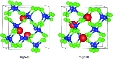 |
| | Fig. 1 Doped I2d-CN2 structures with substitution of N and C by three Ti atoms. | |
The optical properties can be calculated from the complex dielectric function, ε(ω) = ε1(ω) + iε2(ω), based on the re-optimized crystal geometry. Herein, the ε2(ω) can be calculated from the momentum matrix elements of the unoccupied and occupied states,18–20 while the ε1(ω) is derived from ε2(ω) based on Kramers–Krönig transformation. All the optical constants can be obtained using the dielectric function.21–24
The elastic constants are obtained using strain–stress relationship25 as implemented in VASP. In the stress–strain method, the stress is calculated as a function of the strain, with the internal coordinates optimized under each strain condition. The elastic constants of the structure describe its response to an applied stress or the stress required to maintain a given deformation. Technically, in order to determine the Hessian matrix under the external force, we use IBRION = 6, which considers the symmetry of structures. In consideration of the structural deformation under the external force, ISIF = 3 is also used in calculations. For a crystal structure to be mechanically stable, the necessary conditions for tetragonal crystal structure are given as follows:26,27
| | |
Cij > 0, (C11 − C12) > 0, (C11 + C33 − 2C13) > 0, (2C11 + C33 + 2C12 + 4C13) > 0.
| (1) |
Further information on the bulk modulus (G), shear modulus (B), Young's modulus (E) and hardness can be derived from elastic constants.
3. Results and discussion
3.1 Dynamic stability
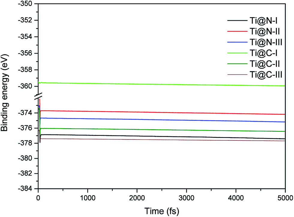
The dynamic stability of the Ti-doped structures is presented in the Fig. 2. We find that all the structures are stable by the Ab initio molecular dynamics calculations, and their stabilities are comparable with each other. When the doping concentration reaches a maximum, the change of Ti-doped structures is small compared with that of the structures shown in Fig. 1. Therefore, all the doping structures still hold dynamic stability.
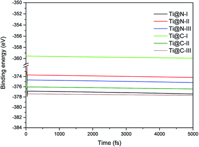 |
| | Fig. 2 MD energies of Ti-doped I2d-CN2 structures in 5 ps (5000 fs) with a time step of 1 fs. | |
3.2 Carrier mobility
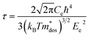
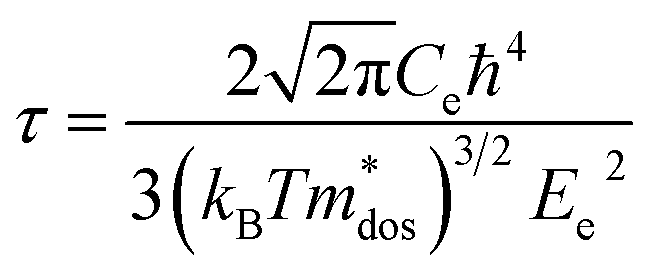
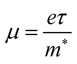
To evaluate the electronic transport coefficients by Boltzmann transport theory and relaxation time approximation, the relaxation time and carrier mobility have to be determined, which are usually complicated since they depend on the detailed scattering mechanisms. The scattering of carriers is dominated by the electron–acoustic phonon coupling.28 In this respect, we evaluate the relaxation time with deformation potential theory, which can give a good description on the electron–acoustic phonon interactions. For the three-dimensional structure, the relaxation time τ and carrier mobility μ at the temperature of 300 K can be expressed as follows:29| |
 | (2) |
| |
 | (3) |
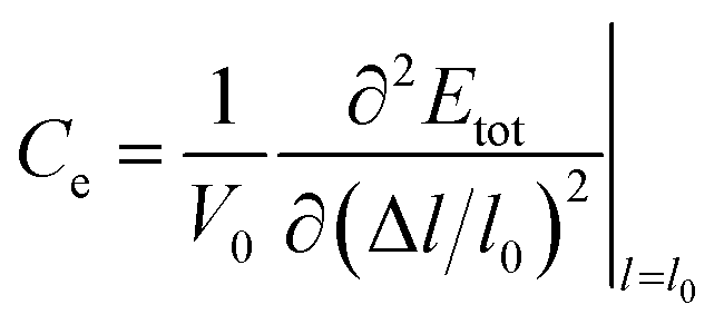
where Ce is the elastic constant defined as  , in which Etot is the total energy of the structure, l0 is the lattice constant, Δl is the corresponding lattice distortion, and V0 is the equilibrium volume of the system. The deformation potential30,31 constant Ee is calculated as
  , which represents the shift of band edges per unit strain. The density of states effective mass
  is expressed as
  , in which
  ,
,  , and
, and  represent the effective mass along x, y, and z directions, respectively. All the three quantities (Ce, Ee, and
  ) are obtained from first-principles calculations. The calculated relaxation time τ and carrier mobility μ for pristine and doped systems are summarized in Table 1. Compared with that of pristine I2d-CN2, the relaxation time of doped systems is significantly decreased due to the introduction of impurity Ti atom. Further calculations demonstrate that the μs also decreases significantly. On comparing the results for the two doping ways, one can find that both the carrier mobilities and relaxation times of Ti@C are larger than those of Ti@N, which shows that Ti@C or Ti@N are not suitable as solar cell materials, but they may be appropriate for photothermal conversion device material because of the significant enhancement of absorption in the visible light range.
Table 1 Calculated values of elastic constant (Ce), deformation potentials (Ee), effective mass ( ), relaxation time (τ) and carrier mobility (μ) at 300 K
| |
Ce (eV Å−3) |
Ee (eV) |

(me) |
τ (fs) |
μ (cm2 V−1 s−1) |
| Pristine |
9.04 |
31.79 |
1.01 |
48.73 |
84.55 |
| Ti@N-I |
2.85 |
18.92 |
7.99 |
1.96 |
0.43 |
| Ti@N-II |
2.19 |
18.53 |
15.50 |
0.58 |
0.07 |
| Ti@N-III |
11.38 |
37.03 |
14.05 |
0.88 |
0.11 |
| Ti@C-I |
2.67 |
20.28 |
3.23 |
6.24 |
3.40 |
| Ti@C-II |
2.39 |
19.39 |
1.77 |
15.06 |
15.01 |
| Ti@C-III |
2.95 |
22.82 |
4.07 |
3.84 |
1.66 |
3.3 The geometrical structures of the pristine and Ti-doped I2d-CN2
The lattice parameters of the optimized structures are collected in Table 2. From the table, one can find that the lattice parameters of the CN2 structure are changed by the doped Ti atom. As the doping concentration increases, all the lattice parameters become larger with different magnitudes in comparison with that of the pristine I2d-CN2 structure, although the low concentration of dopant has little impact on the lattice parameters. The a, b and c parameters of Ti@N-III reach 6.80 Å, 6.95 Å and 6.92 Å, corresponding to the increase of 5.4%, 7.7% and 0.9%, respectively, in comparison with those of the pristine structure, while the increase of lattice parameters for Ti@C-III are 6.5%, 8.7%, and 0.6%, respectively. The optimized volume (V) for each structure is also included in Table 2. They are accordingly increased in comparison with that of the pristine I2d-CN2.
Table 2 Calculated values of optimized volume (V), total energy (Etot), formation energy (Ef), lattice parameters (L) and energy band gap (Eg)
| |
V (Å3) |
Etot (eV) |
Ef (eV) |
L (Å) |
Eg (eV) |
| a |
b |
c |
GGA + PBE |
HSE |
| I2d-CN2 |
285.37 |
−376.00 |
— |
6.45 |
6.45 |
6.86 |
3.67 |
5.39 |
| Ti@N-I |
303.61 |
−373.66 |
5.19 |
6.59 |
6.60 |
6.89 |
0.35 |
1.56 |
| Ti@N-II |
299.80 |
−370.82 |
8.30 |
6.81 |
6.64 |
6.93 |
1.21 |
1.91 |
| Ti@N-III |
326.39 |
−370.47 |
10.29 |
6.80 |
6.95 |
6.92 |
0.35 |
1.38 |
| Ti@C-I |
299.41 |
−373.36 |
5.60 |
6.57 |
6.61 |
6.88 |
2.87 |
3.16 |
| Ti@C-II |
313.05 |
−372.75 |
10.13 |
6.71 |
6.73 |
6.93 |
2.07 |
3.13 |
| Ti@C-III |
332.11 |
−373.25 |
13.07 |
6.87 |
7.01 |
6.90 |
1.61 |
2.16 |
To evaluate the energy stability of the doped structures and the feasibility of the doping behavior, we calculate formation energy Eform with the following formula.32,33
| | |
Eform(q) = Etot[doped CN2] − Etot[CN2] − E[Ti] + E[M],
| (4) |
where
Etot[doped CN
2],
Etot[CN
2],
E[Ti] and
E[M] represent the total energy of doped I2d-CN
2, the total energy of pristine I2d-CN
2, the energy of dopant Ti atom and the energy of the replaced C or N atom, respectively. The results are included in
Table 2. Generally, the
Eforms of Ti@N structures are smaller than those of Ti@C. Therefore, the N-doped way is easier to prepare with respect to energy. For example, the largest
Eform for the Ti@N structures is 10.29 eV, while the
Eform of Ti@C-III reaches 13.07 eV, which implies that Ti@C-III structure is more difficult to prepare than Ti@N-III structures.
3.4 The electronic properties
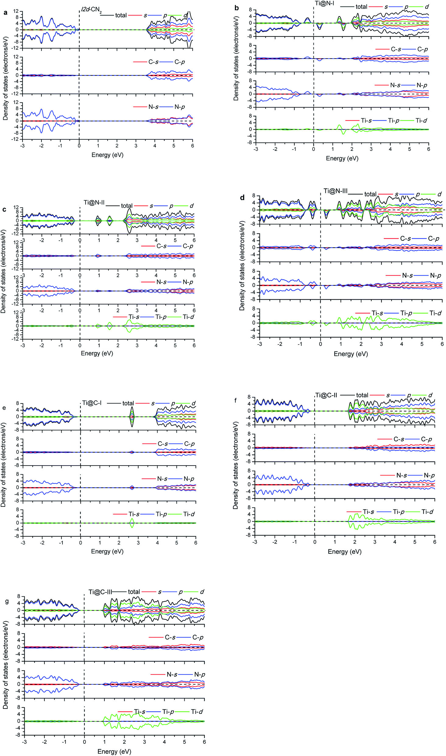
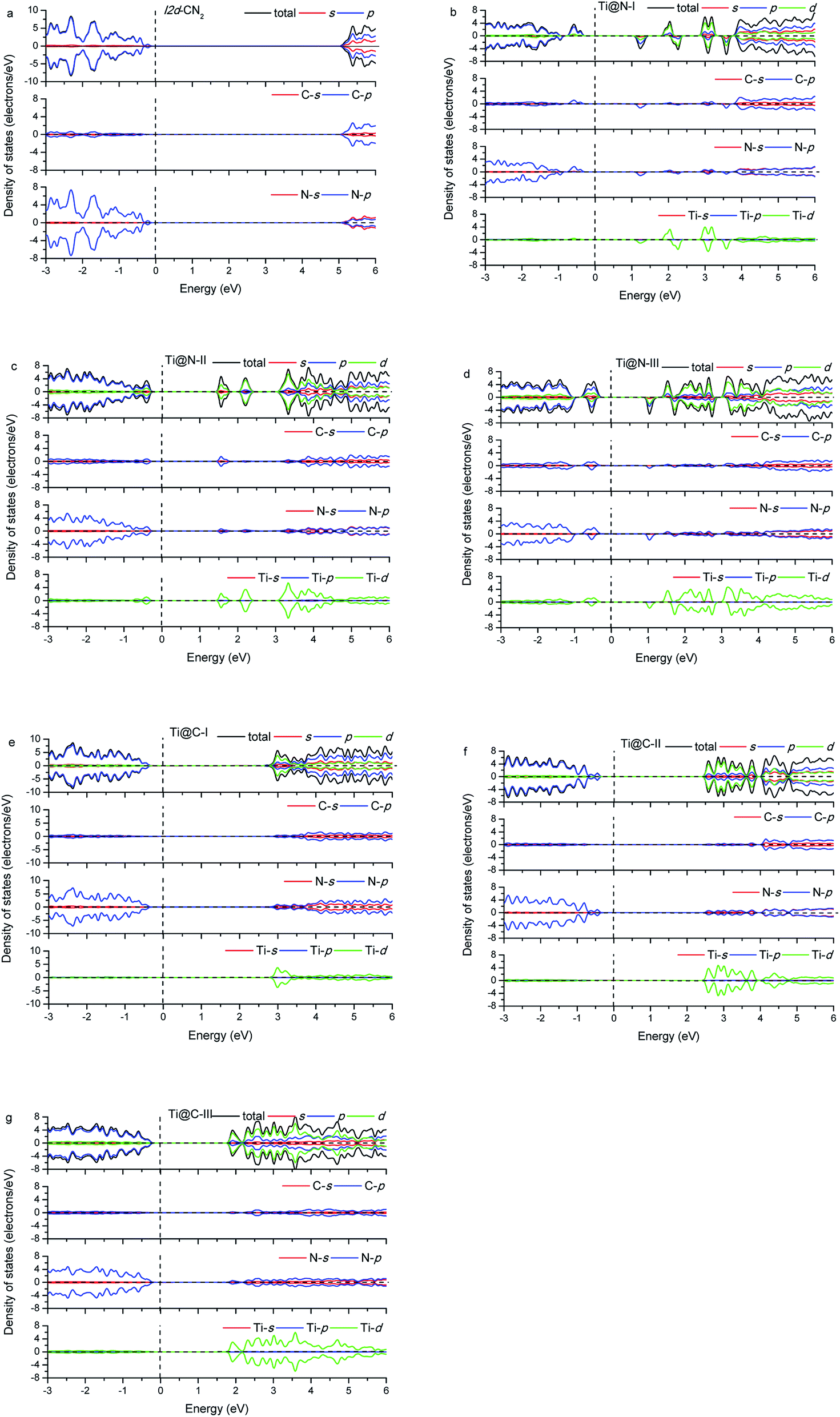
The calculated energy band gap (Eg) of the pristine I2d-CN2 is 3.67 eV with the GGA + PBE method, which is in agreement with the previous theoretical values,8,9 while Eg is 5.39 eV with HSE method. The density of states (DOS) and partial density of states (PDOS) of the pristine and the doped I2d-CN2 structures with GGA + PBE and HSE methods are shown in Fig. 3 and 4, respectively. Fig. 3(a) shows that there is no spin polarization for the pristine I2d-CN2. The top of the valence band (VB) is mainly composed of N-2p state, while the bottom of the conduction band (CB) is dominated by the C-2p state. For the one Ti atom doped structure Ti@N-I, an evident behavior of spin polarization is observed, as shown in Fig. 3(b). It is a result of the unpaired electron of the doped-N atom because the doped-Ti atom results in an odd number of N atoms. The obvious impurity states located at about 1.25 eV for the spin up DOS and 1.5 eV for the spin down DOS can be observed in the CB. It is not difficult to find that the impurity states are mainly composed of Ti-3d state in the figure. The bottom of CB is located at about 0.15 eV and a peak appears at about 0.25 eV for the spin down DOS, which implies that the peak is caused by the orbital hybridization of 2p states. Carefully examining the partial density of states one can find that the peak is composed of C-2p and N-2p. However, for the spin up DOS, the top of VB is located at −0.20 eV below the Fermi level. Therefore, the band energy gap of Ti@N-I decreases to 0.35 eV. For the larger concentration of Ti@N-II structure, Fig. 3(c) shows that the spin polarization completely disappears, which can be understood by the DOS returning to pair because the total electronic number becomes an even number along with the N atoms becoming an even number. However, the spin polariton appears again for the Ti@N-III structure, as shown in Fig. 3(d). All the C-2p, N-2p, and Ti-3d states contribute to the spin up and spin down DOSs of the top of VB, although the spin up DOS has two peaks and is a little larger than the spin down one. For the bottom of CB, only spin down DOS is observed at 0.15 eV first but no spin up DOS, implicating significant spin polarization, which leads to smaller band energy gaps of 0.35 eV. Compared with Ti@N-I, the changes are about 0.5–2.5 eV of CB and around −0.4 eV in VB. From the DOS in Fig. 3 and 4, one can find that the impurity states of Ti atoms significantly decrease the band gap of I2d-CN2 and mainly contribute to the conduction band minimum. However, unlike the case of N-doped TiO2,34 the DOS overlap between the d state of Ti and the s and p states of C and N are small, indicating that the electrons in Ti are difficult to transfer to C or N atoms.
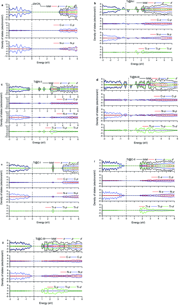 |
| | Fig. 3 Density of states with GGA + PBE. | |
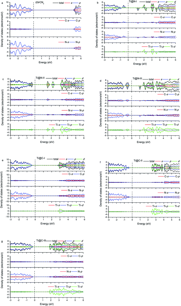 |
| | Fig. 4 Density of states with HSE. | |
In the case of Ti substituting C atom, as shown in Fig. 3, no spin polarization phenomenon is observed for all the considered structures owing to the even number of electrons for both Ti and C atoms. Fig. 3 shows that the N-2p state always occupies the top of VB, and the Ti-3d state occupying the bottom of CB increases gradually with the concentration of Ti, whereas the N-2p state loses the leading role evidently at bottom of the CB. Furthermore, we can find that the band energy gap gradually decreases with rising concentration of Ti to Ti@C-III, as shown in Fig. 3(g). Generally, the Ti-3d states significantly contribute to the bottom of CB in all the three doped I2d-CN2 structures, which decrease band energy gap. However, the narrow effect of band energy gap is significantly smaller than that of the Ti substituting N atoms, particularly for concentrations with the spin polarization phenomenon.
Comparing with the GGA + PBE method, there are some differences for the DOSs of HSE. Clearly, the band energy gaps enlarge significantly compared with those of GGA + PBE method in the same concentrations. Second, the first peaks of Ti@N-I in Fig. 4(b) and Ti@N-III in Fig. 4(d) at about 0.25 eV move to 1.2 eV and 1.0 eV, respectively. From the Ti-doped DOSs of HSE, we also find the same tendency in Ti@C (Fig. 4(e)–(g)) compared with that of the GGA + PBE method. In short, the CBs of Ti@N and Ti@C calculated with HSE appear blue shifted compared with those of GGA + PBE method.
3.5 Dielectric function, absorption, and photoconductivity
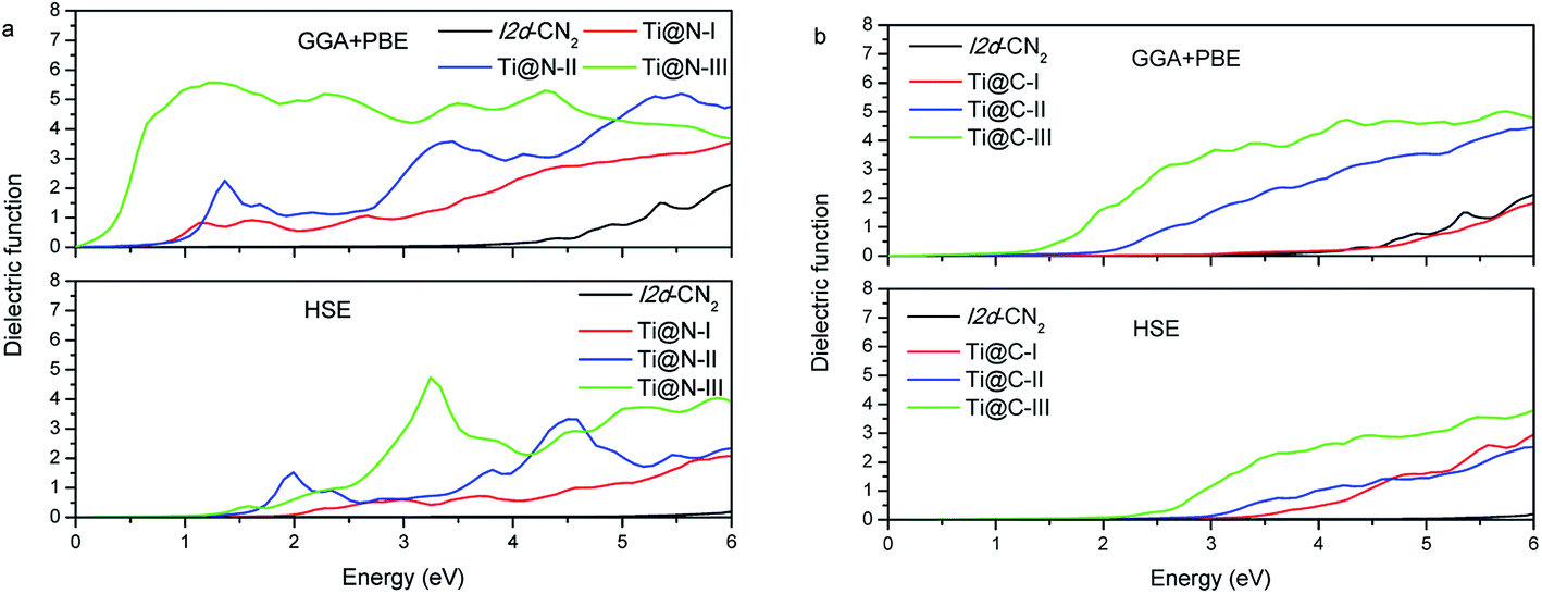
The optical properties can be derived from the complex dielectric function, and the real part may be calculated from the imaginary part. Therefore, we calculate the imaginary ε2 first, and the results with the two methods of GGA + PBE and HSE are presented in Fig. 5(a) and (b). The characteristic of the imaginary part ε2 of dielectric function can also be used to understand the DOSs presented in the above section. In GGA + PBE method, for Ti@N-I, there are two evident dielectric peaks at 1.13 eV and 1.61 eV, which correspond to transitions from the peak of −0.90 eV to that of 0.25 eV in the spin down DOS and from the peak of −0.20 eV to that of 1.33 eV in the spin up DOS, respectively. For HSE method, we can see that ε2 appears blue shifted. Moreover, only Ti@N-III has a small peak at about 1.5 eV and an evident peak at about 3.0 eV, which corresponds to transition from the top of VB to the peaks of 1.0 eV and 2.5 eV in CB. From the ε2 of Ti@C-I in Fig. 5(b), the first dielectric peak is located at approximately 3.5 eV, which is related to the interband transition from the peak of N-2p located at −0.63 eV to that of the impurity state of Ti-3d located at 2.70 eV. The dielectric peaks show red shift with increasing concentration to Ti@C-III. The peaks are located at about 2.0 eV and 1.5 eV for Ti@C-II and Ti@C-III, respectively, corresponding to interband transition as in the case of Ti@C-I. Comparing with the results of the GGA + PBE method, the ε2 of HSE only begins to appear in the visible light range in Ti@C-III.
 |
| | Fig. 5 Dielectric function of Ti@N and Ti@C. | |
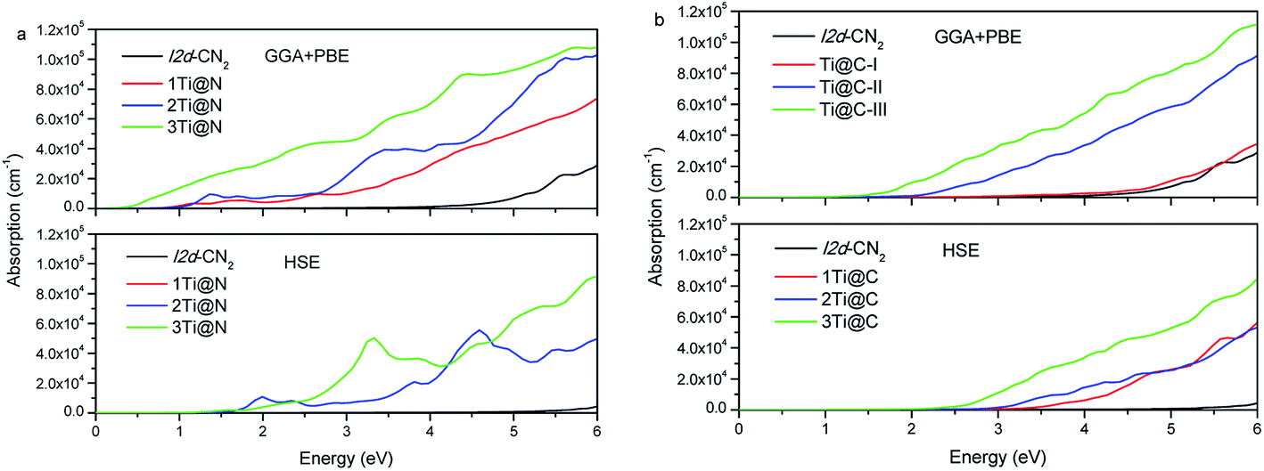
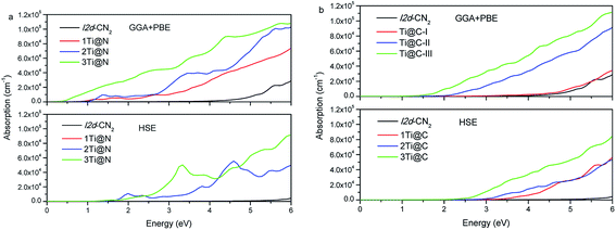
Based on the obtained complex dielectric function, the absorption coefficients of Ti@N and Ti@C structures with GGA + PBE and HSE methods are calculated and shown in Fig. 6. For the GGA + PBE method, the obvious absorption of the pristine I2d-CN2 begins in the ultraviolet range, implicating that the pristine I2d-CN2 cannot harvest solar energy. For the N-doped structures, the obvious absorption can be observed at about 1.1 eV for both Ti@N-I and Ti@N-II, and 0.5 eV for Ti@N-III, which is consistent with the tendency of the dielectric functions, as shown in Fig. 5(a). From the DOSs and PDOSs in Fig. 3, one can understand that the transition from N-2p to Ti-3d state mainly contributes to the absorption. Hence, the doped-Ti atoms play a direct role in the absorption enhancement in the lower energy range. For the HSE method, we can see that absorptions appear blue shift, same as their dielectric function. As concentration reaches up to Ti@N-III, the absorption increases in the high visible light range and reaches up to 5.0 × 104 cm−1. For the Ti@C structures calculated with the GGA + PBE method, as shown in Fig. 6(b), the absorption of Ti@C-I has no significant difference in comparison with that of the pristine I2d-CN2 because the obvious impurity states are located at about 2.6 eV as shown in the Ti@C-I of Fig. 3(e). However, the absorption enhancement can also be obvious in the visible light for Ti@C-III. For the results calculated with HSE method, although the concentration reaches Ti@C-III, there is no significantly enhanced absorption in visible light range. Comparing the results of Ti@C with those of Ti@N, one can find that the absorption of Ti@N is evidently stronger than that of Ti@C by 6.0 eV, although the two doped ways can significantly enhance the absorption of the visible light range when two or three Ti atoms are doped. Generally speaking, GGA + PBE method often underestimates the band gap, while the HSE method overestimates it. The calculation with the two methods indicates that Ti-doped structures with high doping concentration can be used to harvest solar energy.
 |
| | Fig. 6 Absorption coefficients of (a) Ti@N and (b) Ti@C. | |
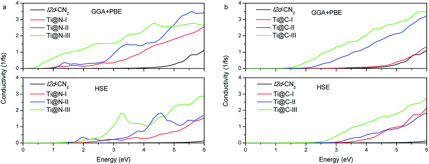
We further investigate the photoconductivity for the doped I2d-CN2 structures. The conductivity is caused by the mobile carriers. In other words, it is closely related to electronic transition. Therefore, the photoconductivity can also be calculated from the dielectric functions. As shown in Fig. 7, it is not difficult to find that photoconductivity has the same tendency as the change of absorption under the same concentration. There is no conductivity in the visible light range for pristine I2d-CN2 structure, but an obvious conductivity can be observed in the range for the doped structures. Comparing Fig. 7(a) and (b), we find that Ti@N, particularly heavily doped Ti@N-III, has stronger conductivity in the infrared region and visible light range for the GGA + PBE method, while no conductivity is observed in the infrared region, even for higher concentration structure Ti@C-III. Comparing with the results calculated by GGA + PBE method, the conductivity calculated with HSE method is small same as the change of its absorption in the low visible light range. Hence, they both are expected to be light-sensitive semiconductor materials in the high part of the visible light range.
 |
| | Fig. 7 Photoconductivity of (a) Ti@N and (b) Ti@C. | |
3.6 The effect of dopant on the elastic properties
Elastic constants are extremely important due to their close relations with various fundamental physical properties.35 To examine the influence of the dopant on the elastic properties, we further calculate the elastic constant Cij. First, we calculate the elastic constant of super-cell for pristine I2d-CN2 and show the results in Table 3. The elastic constants and the elastic modulus are in agreement with the result of Dong et al.9 The elastic constants of the doped structures are also included in Table 3. The result shows that the calculated elastic constants (C11, C12, C13, C44, C55, and C66) for Ti doped I2d-CN2 structures satisfy the mechanical stability criteria,26,27 implying that all the structures are stable mechanically. Generally, the elastic constants C11 and C33 have a relationship with the resistances to linear compression in x and z directions, respectively. The other independent constants C12, C13, C44, and C66 are related to the elasticity in shape. Table 3 shows that the value of C33 is higher than C11 for all Ti doped I2d-CN2 structures, which means that the structures are more difficult to be compressed along the z-axis than along the x-axis.36
Table 3 The calculated elastic constants (Cij in GPa), bulk modulus (B in GPa), shear modulus (G in GPa), Young's modulus (E in GPa) and Vickers hardness in Chen model (HV in GPa)
| |
Elastic constants |
B |
G |
E |
HV |
| C11 |
C33 |
C44 |
C66 |
C12 |
C13 |
| Pristine |
788, 741![[thin space (1/6-em)]](https://www.rsc.org/images/entities/char_2009.gif) 9 9 |
1239, 11879 |
356, 3639 |
382, 3349 |
224, 2069 |
150, 1399 |
423, 3989 |
357, 3529 |
836, 8159 |
48.0, 50.3 9 |
| Ti@N-I |
668 |
1001 |
248 |
307 |
191 |
136 |
359 |
272 |
651 |
35.3 |
| Ti@N-II |
535 |
904 |
243 |
184 |
179 |
166 |
325 |
222 |
543 |
27.3 |
| Ti@N-III |
501 |
715 |
227 |
222 |
197 |
176 |
310 |
208 |
510 |
25.5 |
| Ti@C-I |
897 |
1196 |
395 |
350 |
481 |
324 |
582 |
335 |
1106 |
28.5 |
| Ti@C-II |
594 |
955 |
143 |
246 |
187 |
157 |
344 |
193 |
488 |
19.2 |
| Ti@C-III |
490 |
681 |
136 |
237 |
191 |
202 |
313 |
165 |
422 |
15.8 |
The polycrystalline bulk modulus (B) and shear modulus (G) can be derived using the Voigt–Reuss–Hill (VRH) approximations.37–39 The Voigt (V) approximation38 gives the upper limit for the parameters that are expressed through elastic coefficient Cij. The Reuss (R) approximation39 gives the lower limit through the elastic compliance tensor Sij. The average of the two limits works as the Hill approximation37 and provides more reliable bulk and shear modulus. The bulk and shear modulus can be expressed with Voigt and Reuss approximations as follows:
| | |
BV = (2(C11 + C12) + C33 + 4C13)/9,
| (5) |
| | |
GV = (M + 3C11 − 3C12 + 12C44 + 6C66),
| (6) |
| | |
GR = 15(18BV/C2 + 6/(C11 − C12) + 6/C44 + 3/C66)−1,
| (8) |
where
M =
C11 +
C12 + 2
C33 − 4
C13 and
C2 = (
C11 +
C12) ×
C33 − 2
C13C13. Using the above Voigt and Reuss limits, we can obtain the Hill approximation of bulk modulus (
BH) and shear modulus (
GH):
The Young's modulus (E) is
Based on Chen model, one can obtain the Vickers hardness (HV) as follows:12
| | |
HV = 2(k2G)0.585 − 3,
| (12) |
Here,
k and
G represent Pugh's modulus ratio (
k =
G/
B) and shear modulus, respectively. Our results for the pristine I2d-CN
2 structure are in good agreement with that of Dong
et al. Hence, we further calculate the elastic constants, elastic modulus and
HV for the Ti doped structures of Ti@N and Ti@C.
Table 3 shows that
B,
G,
E, and
HV decrease along with the increase in the Ti-doped concentration. For example, the
E decreases from 815 GPa of pristine I2d-CN
2 structure to 510 GPa of Ti@N-III and 422 GPa of Ti@C-III structures. The clear decrease of
E implies that the covalent bond in the Ti-doped structures becomes weak because
E is relative to the covalent nature of a structure. Generally, the Ti-doped performance results in the hardness decrease of I2d-CN
2. The modules will be lower than the super-hard criteria even if one Ti atom is doped. Moreover, the decrease of Ti@C structures are more obvious than those of Ti@N structures. When the optical absorptions are significantly enhanced in the visible light range, the Ti@N-III and Ti@C-III structures are still highly hard materials although their
HVs decreases to 25.5 and 15.8 GPa, respectively. Therefore, the Ti-doped I2d-CN
2 could be a candidate for hard-wearing solar energy harvest or photocatalytic materials.
After examining the formation energy, the optical properties, and the hardness, we can draw a conclusion that the Ti@N structures are more favorable materials with their lower formation energy, stronger absorption in the infrared and visible light range, and larger hardness in comparison with those of Ti@C structures.
4. Conclusion
In summary, the effects of the doped Ti element on the mechanical and optical properties of I2d-CN2 are determined. The doped-Ti atoms can significantly affect the carrier mobility and electronic properties, particularly, the spin polarization effects are observed for the Ti@N-I and Ti@N-III structures. The results of the electronic properties show that Ti-3d state makes a contribution to interband transition. In the visible light range, the results by both GGA + PBE and HSE methods demonstrate a significant absorption enhancement achieved for both Ti@N and Ti@C at a concentration of 6.25%, although the enhancement for the latter is relatively weaker. Therefore, they can be used as candidate materials to harvest solar energy. The considerable photoconductivity in the visible light is observed in some of the doped structures, which implies that they can also be used as light-response materials. The results of the mechanical properties show that the hardness decreases gradually along with the increase of concentrations for both Ti@N and Ti@C structures. For the same concentration, the hardness of Ti@N is higher than that of Ti@C. The Ti@N structures are more favorable than the Ti@C structure due to their smaller formation energy, stronger absorption in the infrared and visible light range, and larger hardness. The findings provide helpful information to design and prepare the high hard optical materials based on I2d-CN2.
Conflict of interest
There are no conflicts of interest to declare.
Acknowledgements
This study was supported by the National Science Foundation of China (NSFC) under Grant No. NSFC-11574125 and NSFC-11374132, as well as the Taishan Scholars project of Shandong Province (ts201511055).
References
- A. Y. Liu and M. L. Cohen, Science, 1989, 245, 841–842 CAS
 .
. - A. Y. Liu and M. L. Cohen, Phys. Rev. B: Condens. Matter Mater. Phys., 1990, 41, 10727–10734 CrossRef CAS .
- M. L. Cohen, Phys. Rev. B: Condens. Matter Mater. Phys., 1985, 32(12), 7988 CrossRef CAS .
- Q. Li, Y. Ma, A. R. Oganov, H. Wang, H. Wang, Y. Xu, T. Cui, H. Mao and G. Zou, Phys. Rev. Lett., 2009, 102, 175506 CrossRef PubMed .
- Q. Li, M. Wang, A. R. Oganov, T. Cui, Y. Ma and G. Zou, J. Appl. Phys., 2009, 105, 053514 CrossRef .
- R. Weihrich, S. F. Matar, E. Betranhandy and V. Eyert, Solid State Sci., 2003, 5(5), 701–703 CrossRef CAS .
- R. Weihrich, V. Eyert and S. F. Matar, Chem. Phys. Lett., 2003, 373(5), 636–641 CrossRef CAS .
- Q. Li, H. Y. Liu, D. Zhou, W. T. Zheng, Z. J. Wu and Y. M. Ma, Phys. Chem. Chem. Phys., 2012, 14(37), 13081–13087 RSC .
- H. F. Dong, A. R. Ognaov, Q. Zhu and G. R. Qian, Sci. Rep., 2015, 5, 9870 CrossRef CAS PubMed .
- A. O. Lyakhov and A. R. Oganov, Phys. Rev. B: Condens. Matter Mater. Phys., 2011, 84, 092103 CrossRef .
- K. Li, X. Wang, F. Zhang and D. Xue, Phys. Rev. Lett., 2008, 100, 235504 CrossRef PubMed .
- X. Q. Chen, H. Niu, D. Li and Y. Li, Intermetallics, 2011, 19, 1275–1281 CrossRef CAS .
- Z. C. Zhao, C. L. Yang and M. S. Wang, J. Comput. Electron., 2017, 16(2), 262–271 CrossRef CAS .
- J. P. Perdew, K. Burke and M. Ernzerhof, Phys. Rev. Lett., 1996, 77, 3865 CrossRef CAS PubMed .
- G. Kresse and J. Furthmüller, Phys. Rev. B: Condens. Matter Mater. Phys., 1996, 54, 11169–11186 CrossRef CAS .
- P. E. Blöchl, C. J. Först and J. Schimpl, Bull. Mater. Sci., 2003, 26, 33–41 CrossRef .
- H. J. Monkhorst and J. D. Pack, Phys. Rev. B: Condens. Matter Mater. Phys., 1976, 13, 5188 CrossRef .
- M. Gajdoš, K. Hummer, G. Kresse and J. Furthmüller, Phys. Rev. B: Condens. Matter Mater. Phys., 2006, 73(4), 045112 CrossRef .
- J. E. Sipe and A. I. Shkrebtii, Phys. Rev. B: Condens. Matter Mater. Phys., 2000, 61(8), 5337 CrossRef CAS .
- J. L. Cabellos, B. S. Mendoza and M. A. Escobar, Phys. Rev. B: Condens. Matter Mater. Phys., 2009, 80(15), 155205 CrossRef .
- Y. X. Han, C. L. Yang, J. S. Yang, M. S. Wang and X. G. Ma, Phys. B, 2013, 417, 17–23 CrossRef CAS .
- E. Rita, E. Alves, U. Wahl, J. G. Correia, A. J. Neves, M. J. Soares and T. Monteiro, Phys. B, 2003, 340, 235–239 CrossRef .
- J. C. Ronfard-Haret, J. Kossanyi and J. L. Pastal, J. Phys. Chem. Solids, 2001, 62(3), 565–578 CrossRef CAS .
- T. T. Song, J. He, Q. K. Meng and P. Sun, Chin. J. Comput. Phys., 2008, 3, 17 Search PubMed .
- Y. L. Page and P. Saxe, Phys. Rev. B: Condens. Matter Mater. Phys., 2002, 65, 104104 CrossRef .
- M. Born, Proc. Cambridge Philos. Soc., 1940, 36, 160 CrossRef CAS .
- M. J. Xing, B. H. Li, Z. T. Yu and Q. Chen, RSC Adv., 2016, 6(39), 32740–32745 RSC .
- Y. Q. Cai, G. Zhang and Y. W. Zhang, J. Am. Chem. Soc., 2014, 136, 6269 CrossRef CAS PubMed .
- Q. Y. Xue, H. J. Liu and D. D. Fan, Phys. Chem. Chem. Phys., 2016, 18, 17912 RSC .
- S. H. Wei and A. Zunger, Phys. Rev. B: Condens. Matter Mater. Phys., 1999, 60, 5404 CrossRef CAS .
- Y. H. Li, X. G. Gong and S. H. Wei, Appl. Phys. Lett., 2006, 88(4), 042104 CrossRef .
- Y. X. Han, C. L. Yang, M. S. Wang and X. G. Ma, J. Alloys Compd., 2014, 617, 518–524 CrossRef CAS .
- T. Maeda and T. Wada, Jpn. J. Appl. Phys., 2013, 52(6R), 061201 CrossRef .
- R. Asahi, T. Morikawa and T. Ohwaki, Science, 2001, 293(5528), 269–271 CrossRef CAS PubMed .
- E. Ateser, H. Ozisik, K. Colakoglu and E. Deligoz, Comput. Mater. Sci., 2011, 50, 3208 CrossRef CAS .
- N. Guechi, A. Bouhemadou, R. Khenata, S. Bin-Omran, M. Chegaar, Y. Al-Douri and A. Bourzami, Solid State Sci., 2014, 29, 12 CrossRef CAS .
- R. Hill, Proc. Phys. Soc., London, Sect. A, 1952, 65, 349 CrossRef .
- W. Voigt, Lehrbuch der Kristallpysik Taubner, 1928, p. 29 Search PubMed .
- A. Reuss, Z. Angew. Math. Mech., 1929, 9, 49 CrossRef CAS .
|
| This journal is © The Royal Society of Chemistry 2017 |
Click here to see how this site uses Cookies. View our privacy policy here. 
 Open Access Article
 This Open Access Article is licensed under a
  *a,
Mei-Shan Wanga,
Xiao-Guang Maa,
Li-Bo Zhanb and
You-Gen Yic
*a,
Mei-Shan Wanga,
Xiao-Guang Maa,
Li-Bo Zhanb and
You-Gen Yic

 , in which Etot is the total energy of the structure, l0 is the lattice constant, Δl is the corresponding lattice distortion, and V0 is the equilibrium volume of the system. The deformation potential30,31 constant Ee is calculated as
 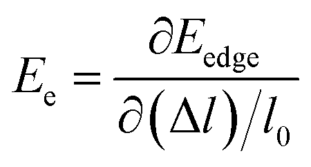 , which represents the shift of band edges per unit strain. The density of states effective mass
  is expressed as
 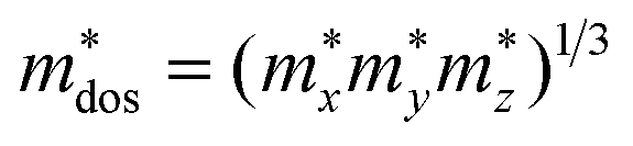 , in which
  ,
,  , and
, and  represent the effective mass along x, y, and z directions, respectively. All the three quantities (Ce, Ee, and
  ) are obtained from first-principles calculations. The calculated relaxation time τ and carrier mobility μ for pristine and doped systems are summarized in Table 1. Compared with that of pristine I2d-CN2, the relaxation time of doped systems is significantly decreased due to the introduction of impurity Ti atom. Further calculations demonstrate that the μs also decreases significantly. On comparing the results for the two doping ways, one can find that both the carrier mobilities and relaxation times of Ti@C are larger than those of Ti@N, which shows that Ti@C or Ti@N are not suitable as solar cell materials, but they may be appropriate for photothermal conversion device material because of the significant enhancement of absorption in the visible light range.
 ), relaxation time (τ) and carrier mobility (μ) at 300 K