
 Open Access Article
 This Open Access Article is licensed under a Creative Commons Attribution-Non Commercial 3.0 Unported Licence
Enhancing the performance and stability of organic solar cells using solution processed MoO3 as hole transport layer
Fei Cheng *,
Yiheng Wu,
Yongcai Shen,
Xueyuan Cai and
Lingli Li
*,
Yiheng Wu,
Yongcai Shen,
Xueyuan Cai and
Lingli Li
School of Physics and Electrical Engineering, Anqing Normal University, Anqing, 246133, P. R. China. E-mail: gcqiuxiong@foxmail.com
First published on 1st August 2017
Abstract
Efficient and stable poly(3-hexylthiophene) (P3HT):indene-C60 bisadduct (ICBA) based bulk-heterojunction (BHJ) organic solar cells (OSCs) with solution processed MoO3 (s-MoO3) as hole transport layer were fabricated. We used a facile and cost-effective preparation method to obtain a MoO3 aqueous solution by thermal decomposition of (NH4)6Mo7O24·4H2O. The s-MoO3 ultra-thin film was treated in three different ways to compare the effects of the annealing mode: no annealing, 100 °C thermal annealing and ultraviolet (UV) annealing. The transmittance, surface morphology and film quality of the s-MoO3 film can be enhanced by UV annealing treatment, which is favorable to the performance of devices. The OSCs with UV annealing treated s-MoO3 as the hole transport layer exhibit a good power conversion efficiency (PCE) of 5.4% and better stability.
1. Introduction
Bulk-heterojunction (BHJ) organic solar cells (OSCs) have attracted great attention in recent years because of their low cost, easy fabrication, simple device structure, promising applications, light-weight properties, potential for large-area devices and their possibility to flex, roll, fold for portability.1–5 In the past few years, in order to achieve commercial application, many efforts have been made to improve the power conversion efficiency (PCE) of BHJ OSCs. Considerable progress has been made in the improvement of these devices, and the achieved efficiencies have evolved from less than 1% in a poly(phenylene vinylene) (PPV) system in 1995,6 to approaching 5% in the most representative (3-hexylthiophene) (P3HT):(6,6)-phenyl-C61-butyric acid methyl ester (PCBM) system in 2005,7–9 to 12.7% in a novel polymer material system in 2017.1 To date, the most traditionally and frequently employed hole transport layer in BHJ OSCs is poly(3,4-ethylenedioxythiophene):poly(styrenesulfonate) (PEDOT:PSS). The reason is that PEDOT:PSS has a good hole transporting ability, high transparency, smooth morphology and high work function, which is suitable for the highest occupied molecular orbital (HOMO) of most donor-type semiconductors.5,10,11 However, the instability of OSCs with PEDOT:PSS as the hole transport layer is not satisfying for their future applications. Firstly, water is easily adsorbed by the PEDOT:PSS layer due to its hygroscopic property. Secondly, the work function of the PEDOT:PSS layer is very sensitive to water. Thirdly, PEDOT:PSS maybe yield inhomogeneous film morphologies and unstable electrical properties. Fourthly, PEDOT:PSS is not an effective electron-blocking layer because of the leakage current to the anode.12–18 To solve these problems, inorganic p-type-like metal oxide materials such as NiO, V2O5, MoO3, WO3, CrOx with high work function and good hole conductivity were developed to try to replace PEDOT:PSS as the hole transport layers. However, relatively expensive vacuum preparation are incompatible with the concept of low-cost, solution-processable and roll-to-roll OSCs. Therefore, there is an urgent demand for the hole transport layer to develop some cost-efficient and simply processed preparation method.For this purpose, solution processed MoO3 (s-MoO3) has drawn great attention as an hole transport layer for OSCs with high-performance, owing to its relatively good hole mobility, environmental stability, and transparency in the range of visible light. Recently, several kinds of preparation methods of s-MoO3 were reported in OSCs.19–25 MoO3 solutions were mainly prepared by hydrate and sol–gel methods. However, on one hand, some methods need high temperature treatment; on the other hand, even if it can be able to obtain the MoO3 solutions, the preparation process is still relatively complex and some organic solvents is not friendly to the environment.
In this work, we provide a simple and cost-effective procedure to prepare a continuous and uniform s-MoO3 layer to act as the hole transport layer for OSCs. We used three kinds of annealing treatment on s-MoO3 film for comparison: no annealing, 100 °C thermal annealing, and UV annealing. Among them, the performance of the s-MoO3 film under UV annealing mode is better. So, the performance of P3HT:ICBA based OSCs could be obtained the optimized PCE of 5.4% and a better air stability. The influence of annealing mode for s-MoO3 thin films in OSCs will be discussed in the views of transmittance, surface morphology, valence state and air stability.
2. Experimental details
Fluorinated tin oxide (FTO) coated glass (R = 12–14 Ω sq−1) was cut into 3 cm w2.5 cm chips as substrates. The chips were ultrasonicated in 30 °C aqueous detergent followed by deionized (DI) water, acetone and then alcohol for 10 min each. The substrates were dried under a stream of nitrogen. Subsequently, the FTO-coated glass substrates were treated for 15 min by UV-O3 in order to ameliorate the hydrophilic property. MoO3 solutions were prepared by a thermal decomposition method using ammonium heptamolybdate (NH4)6Mo7O24·4H2O as a precursor. 0.4 g (NH4)6Mo7O24·4H2O was dissolved in 10 mL DI water. In order to form MoO3 nanoparticles favorably, a small amount of hydrochloric acid was added into the solution providing acidic environment.26–28 The mixed solution was heated at 80 °C for 1 hour in air. (NH4)6Mo7O24·4H2O was decomposed to three components, MoO3, NH3 and H2O. NH3 evaporated into the air and MoO3 is the only solute in the solution. The resulting solution was diluted by DI water to 0.1 wt% concentrations. Then 10 mL solution was took for standby. In order to obtain an ultrasmooth MoO3 thin film, we have added a small amount of PEDOT:PSS (about 0.1 mL) into the solution. PEDOT:PSS has been diluted very seriously. As we all know, PEDOT:PSS is purchased and refrigerated, then spin-coated directly. After serious dilution, it's unlikely a mixed film and it's impossible to act as hole transport layer in the OSCs. In our work, we mainly used the small amount of PEDOT:PSS to increase the surface flatness of s-MoO3 ultra-thin film after spin-coating. Then, the MoO3 solutions were spin-coated onto FTO substrates at 3000 rpm. No annealing treatment, 100 °C thermal annealing treatment and UV annealing treatment for the s-MoO3 films before organic active layer deposition was carried out. In order to reduce the unnecessary loss and some trouble of preparation for the possibility of large scale production in the future, we made a try to prepare the MoO3 thin film by a simpler solution process similar to the method to prepare the commonly used PEDOT:PSS thin film. So, we make PEDOT:PSS as reference. As a comparison, PEDOT:PSS was spin-coated on FTO substrates at 750 rpm for 10 s, then 2000 rpm for 20 s. The resulting PEDOT:PSS film was heated on a hot plate at 80 °C for 15 min and the thickness was about 30–35 nm. Subsequently, the active layer was spin-coated from a solution containing P3HT:ICBA (1![[thin space (1/6-em)]](https://www.rsc.org/images/entities/char_2009.gif) :1, w/w) in chlorobenzene on the top of hole transport layers at 450 rpm for 10 s, then 1000 rpm 20 s (thickness = 210 nm). And then the samples were immediately put into the evaporator to deposit LiF (thickness = 1.5 nm) and Al top electrodes (thickness = 100 nm) under a pressure of about 4 0010−4 Pa. The active area of device is 4 mm2. Finally, the fabricated devices were post annealed at 150 °C under Ar ambient for 10 min in argon-filled glove box.
:1, w/w) in chlorobenzene on the top of hole transport layers at 450 rpm for 10 s, then 1000 rpm 20 s (thickness = 210 nm). And then the samples were immediately put into the evaporator to deposit LiF (thickness = 1.5 nm) and Al top electrodes (thickness = 100 nm) under a pressure of about 4 0010−4 Pa. The active area of device is 4 mm2. Finally, the fabricated devices were post annealed at 150 °C under Ar ambient for 10 min in argon-filled glove box.
The deposition rate as well as the nominal film thickness was monitored with a quartz crystal thickness monitor (TM-400, Maxtek, USA). Using a surface profilometer (FTS2-S4C-3D, Taylor Hobson, UK), the film thicknesses were checked and good agreement was obtained. The morphology of the hole transport layer thin film was characterized by atomic force microscopy (AFM, SPM-9500j3) in tapping mode. The transmittance spectra of films were measured by a UV-visible (vis)-near IR (NIR) spectrophotometer (CARY 5000, Varian, Australia) in the 200–800 nm wavelength range at room temperature. Film crystal structure was characterized by X-ray diffraction (XRD, Bruker Axs, D8 Advance) using CuKα radiation at 40 kV and 40 mA. The compositions and chemical states of the molybdenum oxide films were examined by X-ray photoelectron spectroscopy (XPS, XSAM800). The performances of the devices were determined using a calibrated AM1.5G solar simulator under illumination operating at light intensity of 100 mW cm−2. The current–voltage curves were obtained using a standard source measurement unit (Keithley 2400). From this, the fill factor (FF) and the PCE of the device were calculated. The used polymers' chemical structures, the schematic diagram of proposed OSC, and the energy level diagram of materials are shown in Fig. 1.
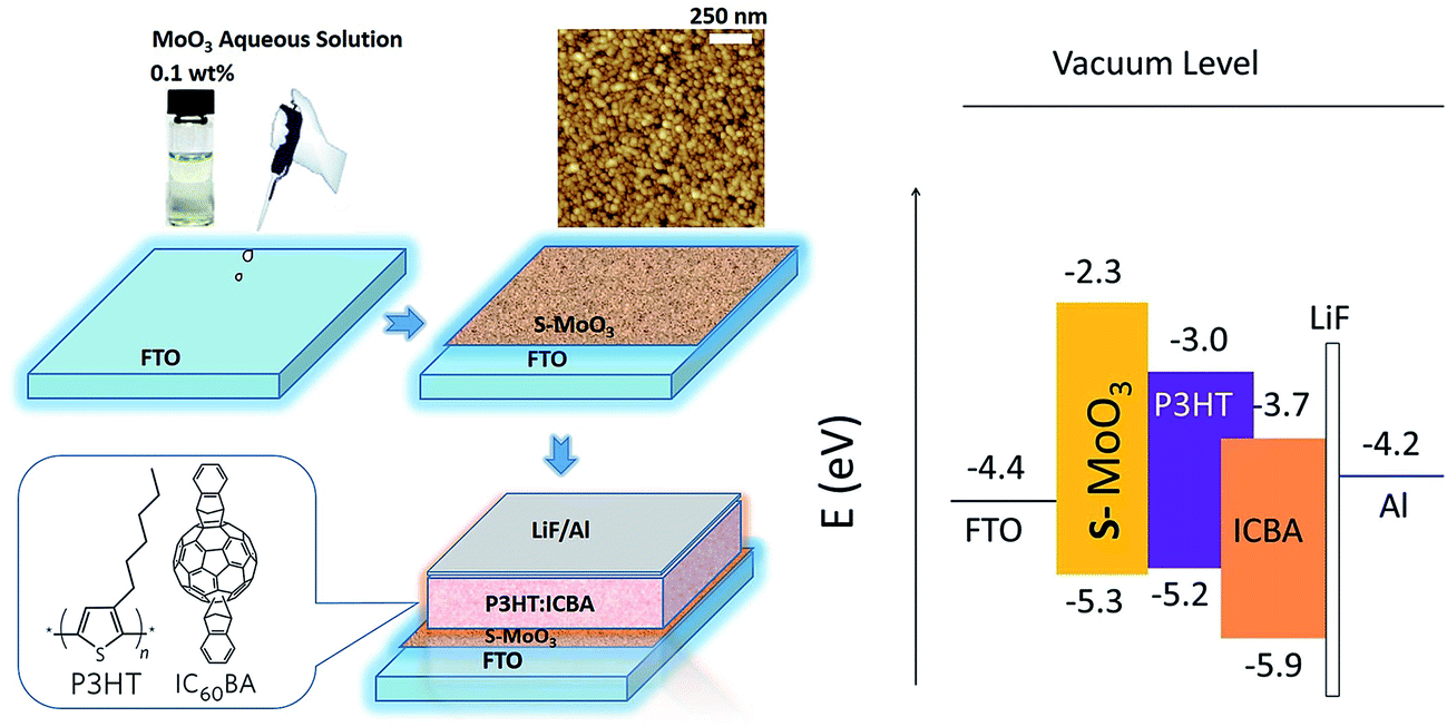 | ||
| Fig. 1 Chemical structures of P3HT and ICBA, device structure of the proposed polymer solar cell, and energy diagram of the OSC devices. | ||
3. Results and discussion
The PCE of the OSCs based on P3HT:PCBM reached over 4% (ref. 7–9) by thermal treatment,7 solvent8 and vapor29 annealing, as well as mixture solvent treatment. However, further improvement of the photovoltaic performance of the OSCs based on P3HT:PCBM is limited because of the relatively small energy difference between the lowest unoccupied molecular orbital (LUMO) of PCBM and the HOMO of P3HT, which results in a lower open circuit voltage (Voc) of the P3HT:PCBM based OSCs to ∼0.6 V.30 In order to further improve device performance, a novel ICBA31–34 with a higher LUMO energy level of −3.74 eV which is higher than that of PCBM was employed as photovoltaic electron acceptor with matching up P3HT as photovoltaic electron donor. In theory, it will results in a higher Voc and PCE in the P3HT:ICBA based OSCs.LiF ultrathin film acted as electron collecting buffer layer in OSCs. The pre-evaporated LiF buffer layer before the deposition of Al electrode can effectively prevent the Al atoms of high energy from directly bombarding the polymer active layer. LiF was inserted as the cathode buffer layer that can isolate the cathode from the polymer active layers with avoiding forming “C–Al” bond,12 improving the quality of the interface and reducing the recombination probability of the excitons. LiF can decline the work function of the cathode at the interface and provide a good ohmic contact between the polymer active layer and the cathode.35 The series resistance will be decreased, and then the FF of the OSCs will be improved. After inserting a LiF thin film layer, a build-in electric field pointing from Al to polymer will be formed inside the polymer/LiF/Al system. The build-in field can push the electrons passing through the buffer layer. So the short-current density (Jsc) of the cells could also be increased.
At the same time, a buffer layer used for modifying anode plays an important role in the device performance. With the insertion of s-MoO3 thin film layer, the energy levels make it act as an efficient exciton blocking layer to mainly prevent electrons to reaching the anode due to the large energy band gap of s-MoO3. The energy of s-MoO3 and the HOMO energy of P3HT matched well (shown in Fig. 1). Holes can be extracted to anode easily. Therefore, s-MoO3 thin film would play a significant impact on the performance of OSCs.
We mainly discussed the s-MoO3 thin film in the views of annealing mode which affects the performance and the stability of OSCs. In this work, the ultrathin s-MoO3 film was treated by three annealing modes: no annealing, 100 °C thermal annealing and UV annealing.
3.1 Optical characteristics of s-MoO3 films
The UV-visible light absorption spectra of P3HT:ICBA and transmission spectra of PEDOT:PSS and s-MoO3 with different annealing modes on FTO are shown in Fig. 2. In accordance with the condition of device fabrication, we use the thin films with the same states to investigate their absorption and transmission. The transmission characteristics of the anode buffers layer were similar to each other. However, a slight decrease in transmission in s-MoO3 films was observed in the wavelength range of 480–800 nm from UV annealing, thermal annealing to no annealing, which could result in less light loss in the device because of the increase of optical transmission across the entire visible spectrum by ≤10%. As shown in Fig. 2 we can see that the transmittance of s-MoO3 by UV annealing treatment is higher than that of PEDOT:PSS from 450 nm to 650 nm in the main area of the spectra. The amelioration of transmission for hole transport layer could be beneficial to the performance of OSCs. We attribute the increase of optical transmission to the removal of contaminations and the change of refraction in the metal oxide because of different valence state and different surface roughness by UV annealing treatment on s-MoO3 film. As we all know, low pressure UV mercury lamp contains two UV lights with wavelength of 254 nm and 185 nm. The photo energy of these two wavelengths could directly open and cut off the organic molecules covalent bonds, with activating organic molecule and decomposing into ions, free atoms, and excited molecules etc. At the same time, the photo energy of 185 nm wavelength UV light could decompose O2 in the air into O3, and the photo energy of 254 nm wavelength UV light could decompose O3 into O2 and active O. The photosensitized oxidation reaction process is continuous. Under the irradiation of these two short wave UV lights, O3 would be generated and decomposed continually. The active O atoms would be generated continually more and more. Because the active O atom can able to oxidize the activated organic molecules, generate volatile gases (such as CO2, CO, H2O, NO, etc.), and completely remove the adhered organic contaminants on the s-MoO3 film surface.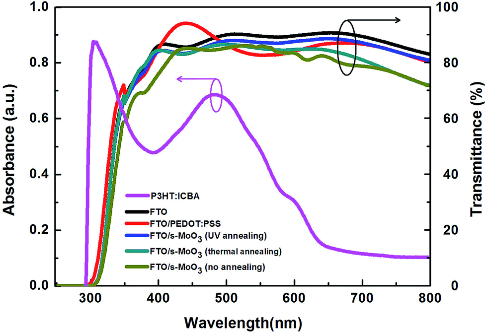 | ||
| Fig. 2 UV-visible light absorption spectra of P3HT:ICBA and transmission spectra of PEDOT:PSS and s-MoO3 with different annealing modes on FTO. | ||
3.2 Surface analysis of s-MoO3 films
Fig. 3 shows the tapping mode AFM micrographs of the FTO/s-MoO3 samples with different annealing modes including only FTO for comparison. It can be seen that the samples of FTO, FTO/s-MoO3 (no annealing), FTO/s-MoO3 (100 °C thermal annealing), and FTO/s-MoO3 (UV annealing) have a surface roughness of 18.68 nm, 17.75 nm, 16.70 nm, and 15.81 nm root-mean-square (rms), respectively.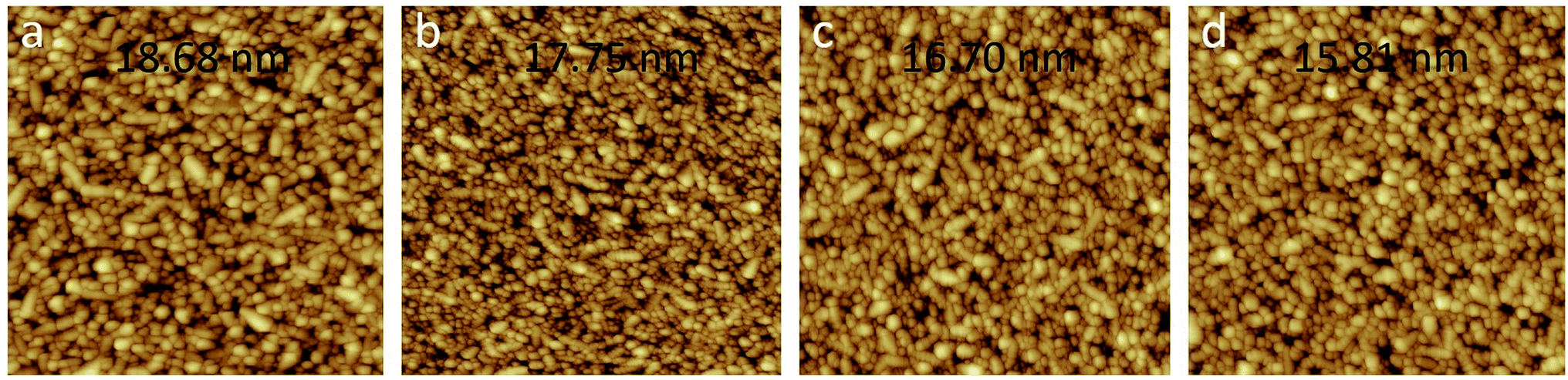 | ||
| Fig. 3 AFM micrographs of the FTO/s-MoO3 samples with different annealing modes including only FTO for comparison: (a) bare FTO, (b) no annealed FTO/s-MoO3, (c) 100 °C thermal annealed FTO/s-MoO3, (d) UV annealed FTO/s-MoO3. | ||
As we all know, besides needing an appropriate device structure, thin film layers in devices are expected as smooth as possible.19 For ultrathin s-MoO3 layers under different annealing modes, each film was found to exhibit similar surface structures as shown in Fig. 3. The decrease of the surface roughness under UV annealing mode may be ascribed to the removal of the contamination as mentioned above.
3.3 X-ray photoelectron spectroscopy of s-MoO3 films
We used XPS to understand the valence state of Mo in s-MoO3 films. Fig. 4 shows the Mo 3d XPS spectra of s-MoO3 films with different annealing modes. As shown in Fig. 4(a) the Mo 3d XPS spectra of s-MoO3 film without annealing treatment contain the peaks of two valence: Mo6+ and Mo5+ divided by the total peak. The Mo6+ fraction calculated as the area under the Mo6+ peaks was 92%. The Mo5+ fraction was 8%. Fig. 4(b) shows the Mo 3d XPS spectra of s-MoO3 film with 100 °C annealing treatment also contain the peaks of two valence: Mo6+ and Mo5+. The Mo6+ fraction was 96% and the Mo5+ fraction was 4%. We can see that after 100 °C annealing treatment the Mo6+ fraction was enhanced. That is to say, the quality of the s-MoO3 film was enhanced. We can foresee that the performance of devices would be improved. From the Fig. 4(c), we can see that the Mo 3d XPS spectra of s-MoO3 film with UV annealing treatment basically only contain the peak of one valence: Mo6+. In other words, relatively pure s-MoO3 film was obtained. So, better performance of devices would be expected.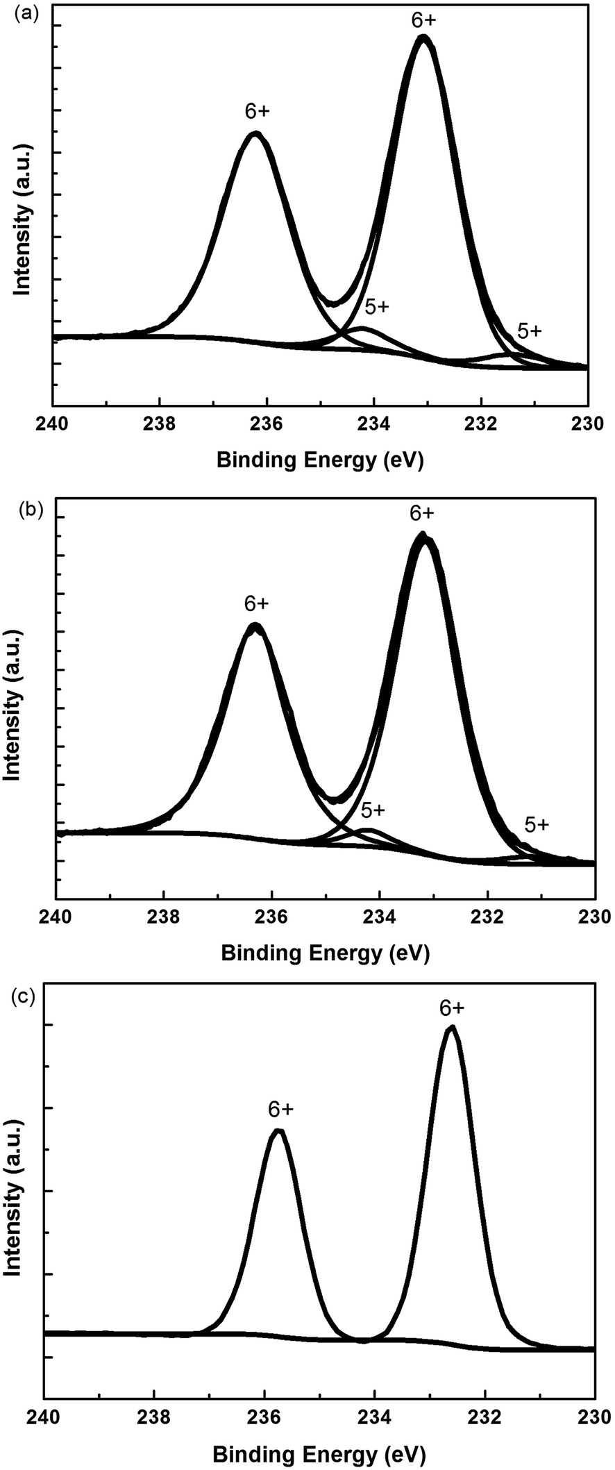 | ||
| Fig. 4 Mo 3d XPS spectra of s-MoO3 films with different annealing modes: (a) no annealing, (b) 100 °C thermal annealing, (c) UV annealing. | ||
3.4 Performance of organic solar cells
To study the effect of different annealing modes on s-MoO3 films, we have fabricated series of devices. Firstly, the structure of FTO/PEDOT:PSS/P3HT:ICBA/LiF/Al was fabricated as a comparison, then the structure of FTO/s-MoO3/P3HT:ICBA/LiF/Al was fabricated with three annealing modes: no annealing, 100 °C thermal annealing and UV annealing to treat the s-MoO3 thin films. The illuminate current density–voltage (J–V) characteristics under AM1.5G illumination (100 mW cm−2) of the OSCs are shown in Fig. 5 and the main extracted performance parameters including Voc, Jsc, FF, PCE are summarized in Table 1. The device with PEDOT:PSS as an hole transport layer showed PCE = 5.22% corresponding to Voc = 0.84 V, Jsc = 11.31 mA cm−2, and FF = 55%. Then, the no annealed s-MoO3 based devices showed PCE = 4.46% with a small decrease in Voc from 0.84 to 0.82 V, a small decrease in FF from 55% to 54% and a larger decline in Jsc from 11.31 to 10.04 mA cm−2 in comparison with that of PEDOT:PSS based devices. When we used 100 °C thermal annealing to treat the s-MoO3 thin film, the performance of devices was improved slightly than that of no annealed s-MoO3 based devices, with the increase in Jsc from 10.04 to 10.67 mA cm−2 and no change in Voc, FF. At last, we adopted the UV annealing to treat the s-MoO3 thin film, there was a larger increase on the performance of the devices in comparison with thermal annealed s-MoO3 based devices. After UV annealing for the s-MoO3 thin film, there was no change in Voc with 0.82 V as before, but there was a large enhancement in Jsc and FF from 10.67 to 11.50 mA cm−2 and 54–58% in comparison with that under thermal annealing mode. Relative to the performance of the devices with PEDOT:PSS as the buffer layer, there was a little decrease in Voc from 0.84 to 0.82 V, but there was a little increase in Jsc, FF from 11.31 to 11.50 mA cm−2, 55–58% respectively. And in the end the PCE was enhanced from 5.22% to 5.4%. It demonstrates that the UV annealed s-MoO3 based devices can get a comparable or even a little better performance than that of PEDOT:PSS based devices.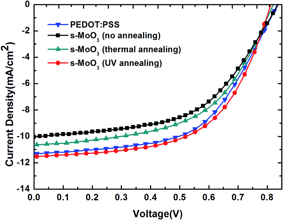 | ||
| Fig. 5 Current density–voltage characteristics of OSCs with PEDOT:PSS and three different annealing modes treated s-MoO3 as the hole transport layers. | ||
| Buffer layer | Voc (V) | Jsc (mA cm−2) | FF (%) | PCE (%) |
|---|---|---|---|---|
| PEDOT:PSS | 0.84 | 11.31 | 55 | 5.22 |
| s-MoO3 (no annealing) | 0.82 | 10.04 | 54 | 4.46 |
| s-MoO3 (100 °C annealing) | 0.82 | 10.67 | 54 | 4.72 |
| s-MoO3 (UV annealing) | 0.82 | 11.50 | 58 | 5.40 |
For Voc, numerous studies have demonstrated that Voc depends on the energy gap between the HOMO level of the donor and the LUMO level of the acceptor of the BHJ, forming the basis for predicting the open circuit voltage in the devices. We used the same active layer so that the value of Voc is very similar. The reason for the little decrease in Voc may be that the work function of PEDOT:PSS is 5.2 eV with matching that of P3HT very well. However, the work function of MoO3 is 5.3 eV. Generally speaking, it is still thought to match that of P3HT well. But the match of MoO3 is not good as that of PEDOT:PSS. So, the devices with s-MoO3 as the hole transport layer showed a little decrease in Voc.
For Jsc, generally speaking, Jsc is mainly determined by the absorption of sunlight by the active layer, the generation of excitons, diffusion, separation, and charge transfer and collection. As shown in Fig. 2 we can see that the transmittance of s-MoO3 by UV annealing treatment is higher than that of PEDOT:PSS from 450 nm to 650 nm in the main area of the spectra. So, it can be foreseen that more light can be absorbed by the active layer. So, the devices with s-MoO3 as the hole transport layer showed a little increase in Jsc.
For FF, as we all known, FF is related to series resistance and shunt resistance. The series resistance, Rs, can be calculated from the inverse slope of the J–V curve in the first quadrant (Fig. 5). On the other hand, the shunt resistance Rsh is determined by the inverse slope of the J–V curve in the fourth quadrant, as shown in Fig. 5. In general, the Rs is smaller and the Rsh is larger, the FF would be larger. From Fig. 5 we can see that the Rs of the device using s-MoO3 by UV annealing treatment as the hole transport layer is smaller than that of the device using PEDOT:PSS as the hole transport layer and the Rsh of the device based on s-MoO3 by UV annealing treatment is larger than that of the device based on PEDOT:PSS. So, the devices with s-MoO3 as the hole transport layer showed a little increase in FF.
3.5 Stability of organic solar cells
Besides the PCE, stability of devices is another important aspect which needs to be enhanced. The performance declines dramatically for unencapsulated devices. As we all know the hygroscopic nature of PEDOT:PSS as the hole transport layer in OSCs may lead to unstable devices. To compare the stability of PEDOT:PSS and s-MoO3 based devices, we measured the J–V characteristics of these un-encapsulated devices over 30 days. As shown in Fig. 6(a)–(d), the performance of devices directly stored in the air could significantly decrease with the increase of storage time. From Fig. 6(e), we can see that the PCE of the standard PEDOT:PSS based devices show a nearly exponential decrease according to the fitting curve. The air stability of the devices with s-MoO3 under three different annealing modes as the buffer layers show drastically enhanced than that of PEDOT:PSS based devices. Comparing with no annealing and 100 °C thermal annealing, the UV annealing for s-MoO3 thin film could improve the air stability of devices. The drastic decrease in performance of devices can be considered to arise from invasion of water and oxygen. The poor stability of PEDOT:PSS based devices can be ascribed to the hygroscopic and acidic nature. So, its performance declines dramatically to near 0 and stays a stable value of 0 with the growth of storage time. MoO3 is regarded as a very stable material which can play as a protective thin film layer with preventing undesired physical and chemical influence. As the storage time continues to grow, the performance of the devices with the s-MoO3 as the hole transport layer will be a stable value of near 0. According to the analysis of XPS above mentioned, the s-MoO3 thin film treated by UV annealing can display the characteristics of MoO3. Eventually, the air stability of the devices can be improved.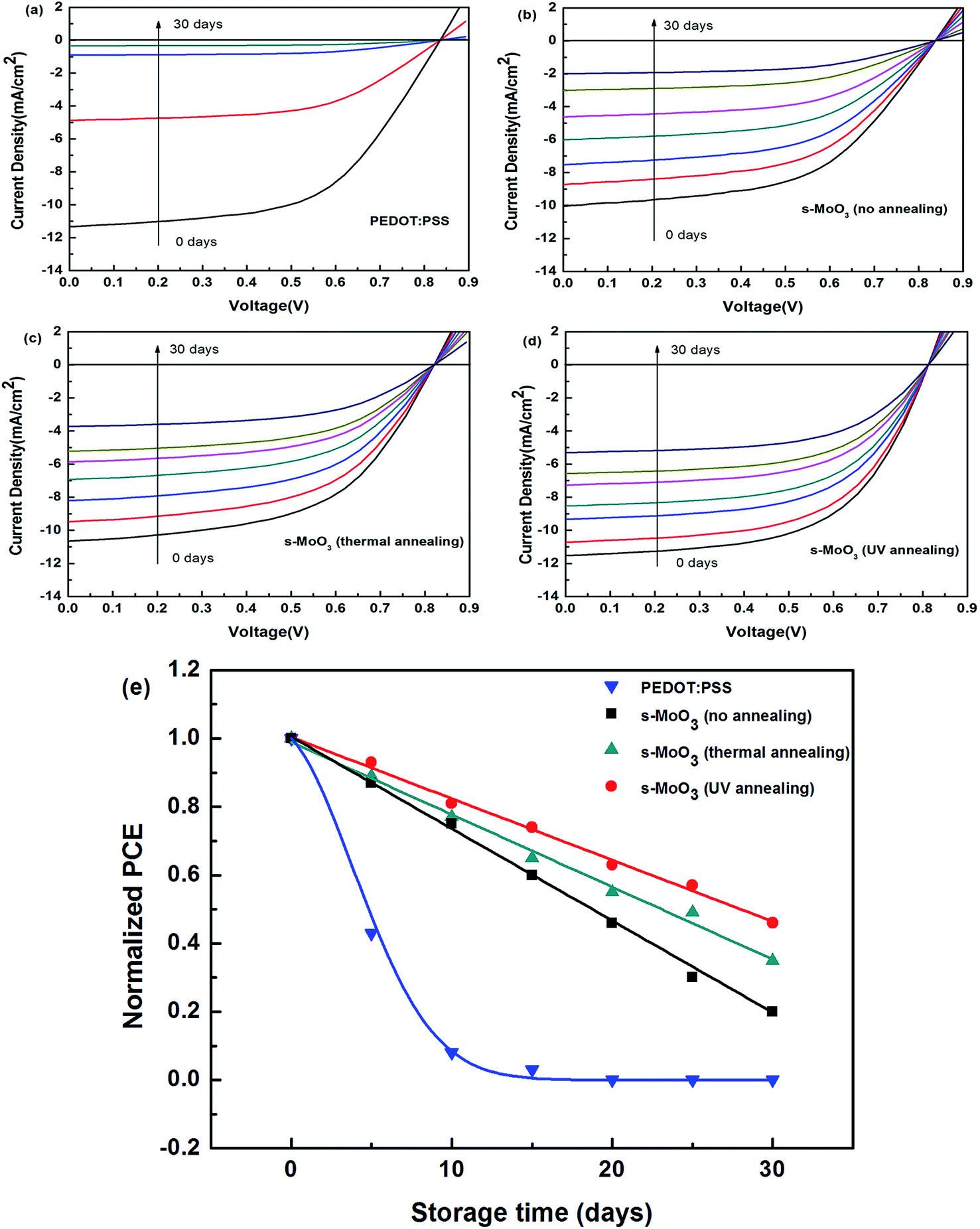 | ||
| Fig. 6 (a)–(d) Change trend of the current density–voltage characteristics of unencapsulated OSCs with PEDOT:PSS and different annealing modes treated s-MoO3 as the hole transport layers with the change of the storage time in ambient air. (e) Normalized PCE of unencapsulated OSCs with PEDOT:PSS and three annealing modes treated s-MoO3 as the hole transport layers with the change of the storage time in ambient air. | ||
4. Conclusion
In conclusion, efficient and stable P3HT:ICBA based BHJ OSCs with s-MoO3 as the hole transport layer was fabricated. We used a facile and cost-effective preparation method to obtain a MoO3 aqueous solution by thermal decomposition of (NH4)6Mo7O24·4H2O. The s-MoO3 ultra-thin film was treated by three annealing modes: no annealing, 100 °C thermal annealing and UV annealing. By UV annealing treatment, the transmittance, surface morphology and film quality of s-MoO3 film can be enhanced which is favorable to the performance of devices. So, the OSCs using s-MoO3 by UV annealing treatment as the hole transport layer can obtain a better PCE and a better stability.Acknowledgements
This work was supported by the Natural Science Research Key Project of Education Department of Anhui Province under Grant No. KJ2017A365 and KJ2017A369, the Doctoral Scientific Research Foundation of Anqing Normal University under Grant No. 044–140001000023.References
- M. Li, K. Gao, X. Wan, Q. Zhang, B. Kan, R. Xia, F. Liu, X. Yang, H. Feng, W. Ni, Y. Wang, J. Peng, H. Zhang, Z. Liang, H.-L. Yip, X. Peng, Y. Cao and Y. Chen, Nat. Photonics, 2017, 11, 85–90 CrossRef CAS
.
- T. Kumari, S. M. Lee, S.-H. Kang, S. Chen and C. Yang, Energy Environ. Sci., 2017, 10, 258–265 CAS
- R. Ji, J. Cheng, X. Yang, J. Yu and L. Li, RSC Adv., 2017, 7, 3059–3065 RSC
- J. Zhao, Y. Li, G. Yang, K. Jiang, H. Lin, H. Ade, W. Ma and H. Yan, Nat. Energy, 2016, 1, 15027 CrossRef CAS
- L. Huo, T. Liu, X. Sun, Y. Cai, A. J. Heeger and Y. Sun, Adv. Mater., 2015, 27, 2938–2944 CrossRef CAS PubMed
- G. Yu, J. Gao, J. C. Hummelen, F. Wudl and A. J. Heeger, Science, 1995, 270, 1789–1791 CAS
- W. L. Ma, C. Y. Yang, X. Gong, K. Lee and A. J. Heeger, Adv. Funct. Mater., 2005, 15, 1617–1622 CrossRef CAS
- G. Li, V. Shrotriya, J. Huang, Y. Yao, T. Moriarty, K. Emery and Y. Yang, Nat. Mater., 2005, 4, 864–868 CrossRef CAS
- M. Reyes-Reyes, K. Kim and D. L. Carroll, Appl. Phys. Lett., 2005, 87, 083506 CrossRef
- C. C. Chen, W. H. Chang, K. Yoshimura, K. Ohya, J. You, J. Gao, Z. Hong and Y. Yang, Adv. Mater., 2014, 26, 5670–5677 CrossRef CAS PubMed
- S. Zhang, L. Ye, W. Zhao, B. Yang, Q. Wang and J. Hou, Sci. China: Chem., 2015, 58, 248–256 CrossRef CAS
- M. Jørgensen, K. Norrman and F. C. Krebs, Sol. Energy Mater. Sol. Cells, 2008, 92, 686–714 CrossRef
- K. Kawano, R. Pacios, D. Poplavskyy, J. Nelson, D. D. C. Bradley and J. R. Durrant, Sol. Energy Mater. Sol. Cells, 2006, 90, 3520–3530 CrossRef CAS
- K. Norrman, M. V. Madsen, S. A. Gevorgyan and F. C. Krebs, J. Am. Chem. Soc., 2010, 132, 16883–16892 CrossRef CAS PubMed
- N. Koch, A. Vollmer and A. Elschner, Appl. Phys. Lett., 2007, 90, 043512 CrossRef
- M. Kemerink, S. Timpanaro, M. M. de Kok, E. A. Meulenkamp and F. J. Touwslager, J. Phys. Chem. B, 2004, 108, 18820–18825 CrossRef CAS
- C. Ionescu-Zanetti, A. Mechler, S. A. Carter and R. Lal, Adv. Mater., 2004, 16, 385–389 CrossRef CAS
- M. D. Irwin, D. B. Buchholz, A. W. Hains, R. P. H. Chang and T. J. Marks, Proc. Natl. Acad. Sci. U. S. A., 2008, 105, 2783–2787 CrossRef CAS
- J. J. Jasieniak, J. Seifter, J. Jo, T. Mates and A. J. Heeger, Adv. Funct. Mater., 2012, 22, 2594–2605 CrossRef CAS
- Y.-J. Lee, J. Yi, G. F. Gao, H. Koerner, K. Park, J. Wang, K. Luo, R. A. Vaia and J. W. P. Hsu, Adv. Energy Mater., 2012, 2, 1193–1197 CrossRef CAS
- S. Murase and Y. Yang, Adv. Mater., 2012, 24, 2459–2462 CrossRef CAS PubMed
- Z. a. Tan, D. Qian, W. Zhang, L. Li, Y. Ding, Q. Xu, F. Wang and Y. Li, J. Mater. Chem. A, 2013, 1, 657 CAS
- M.-F. Xu, L.-S. Cui, X.-Z. Zhu, C.-H. Gao, X.-B. Shi, Z.-M. Jin, Z.-K. Wang and L.-S. Liao, Org. Electron., 2013, 14, 657–664 CrossRef CAS
- C. Yao, X. Xu, J. Wang, L. Shi and L. Li, ACS Appl. Mater. Interfaces, 2013, 5, 1100–1107 CAS
- C. Xu, P. Cai, X. Zhang, Z. Zhang, X. Xue, J. Xiong and J. Zhang, Sol. Energy Mater. Sol. Cells, 2017, 159, 136–142 CrossRef CAS
- X. D. Dong, X. T. Dong, J. H. Liu, J. H. Yan and G. Y. Hong, Rare Met. Mater. Eng., 2005, 34, 837–840 CAS
- F. Liu, S. Shao, X. Guo, Y. Zhao and Z. Xie, Sol. Energy Mater. Sol. Cells, 2010, 94, 842–845 CrossRef CAS
- D. Parviz, M. Kazemeini, A. M. Rashidi and K. Jafari Jozani, J. Nanopart. Res., 2009, 12, 1509–1521 CrossRef
- Y. Zhao, Z. Xie, Y. Qu, Y. Geng and L. Wang, Appl. Phys. Lett., 2007, 90, 043504 CrossRef
- H. Derouiche and V. Djara, Sol. Energy Mater. Sol. Cells, 2007, 91, 1163–1167 CrossRef CAS
- Y. He, H.-Y. Chen, J. Hou and Y. Li, J. Am. Chem. Soc., 2010, 132, 1377–1382 CrossRef CAS PubMed
- G. Zhao, Y. He and Y. Li, Adv. Mater., 2010, 22, 4355–4358 CrossRef CAS PubMed
- Y.-J. Cheng, C.-H. Hsieh, Y. He, C.-S. Hsu and Y. Li, J. Am. Chem. Soc., 2010, 132, 17381–17383 CrossRef CAS PubMed
- C.-Y. Chang, C.-E. Wu, S.-Y. Chen, C. Cui, Y.-J. Cheng, C.-S. Hsu, Y.-L. Wang and Y. Li, Angew. Chem., Int. Ed., 2011, 50, 9386–9390 CrossRef CAS PubMed
- K. L. S. Yanagisawa and Y. Morikawa, J. Chem. Phys., 2008, 128, 244704–244713 CrossRef PubMed
| This journal is © The Royal Society of Chemistry 2017 |