
 Open Access Article
 This Open Access Article is licensed under a
 Creative Commons Attribution 3.0 Unported Licence
A visible high efficiency and polarization-insensitive 34-level dielectric metasurface hologram
Xiaofang Su ab,
Guanhai Li*a,
Hui Yangab,
Zengyue Zhaoac,
Feilong Yuab,
Xiaoshuang Chen*a and
Wei Lua
ab,
Guanhai Li*a,
Hui Yangab,
Zengyue Zhaoac,
Feilong Yuab,
Xiaoshuang Chen*a and
Wei Lua
aNational Laboratory for Infrared Physics, Shanghai Institute of Technical Physics, Chinese Academy of Sciences, 500 Yu Tian Road, Shanghai, 200083, China. E-mail: ghli0120@mail.sitp.ac.cn; xschen@mail.sitp.ac.cn
bUniversity of Chinese Academy of Sciences, No. 19A Yu Quan Road, Beijing, 100049, China
cShanghai University of Science and Technology, 100 Hai Ke Road, Shanghai, 201210, China
First published on 17th May 2017
Abstract
We propose a dielectric metasurface of 34 phase level, to reproduce the holographic image in the visible region. With normal incident circular polarized illumination, imaging efficiency as high as 59.72% is achieved at 560 nm wavelength. Consisting of non-resonant meta-cells, the proposed polarization-insensitive dielectric metasurface performs well in a broad band from 480 nm to 660 nm. Numerical results also indicate that the metasurface hologram maintains high fidelity within a wide-angle incidence (0–25°), and show high tolerance to fabrication errors. The high efficiency, broadband, wide-angle, and high fabrication tolerance metasurface based on the hologram, can be used in the fields of display, security, data storage, and information processing.
Introduction
Metamaterials, constructed from function-driven artificial meta-cells, show great potential in tuning electromagnetic properties, such as the effective electric permittivity and magnetic permeability. Several exotic optical phenomena that are barely found in nature1–9 are also realized with the proposed design. Metasurfaces, two-dimensional metamaterials composed of quasi-periodic arrays of sub-wavelength structures, retain the abilities to manipulate the amplitude, phase and polarization of light upon transmission or reflection. With the superior control over the propagation of electromagnetic waves, metasurface-based vortex generation,10–13 meta-lens,13–19 and wave plates20–22 have been demonstrated recently. Compared with bulk 3D metamaterials, the versatile metasurfaces have smaller physical footprint, simpler fabrication and lower losses. These properties endow the metasurface the capability to move traditional bulky optical elements to deep subwavelength scale and pave the pathway for the realization of opto-electronic integrated devices.Owing to the excellent performance of manipulating electromagnetic waves, metasurface-based holography has been proposed to overcome the defects existing in traditional computer-generated holograms (CGH), for example, low diffraction efficiency caused by unavoidable twin-image and high cost in fabrication procedures because of complicated grayscale lithography. In addition, the working wavelength range is wide due to metasurface's flexibility to engineer the electromagnetic properties. Because of these advantages, metasurface-based holography has attracted continuous scientific interest in recent years.18,23–30 Ni et al.26 demonstrated a 30 nm thick plasmonic metasurface hologram in the visible range, which directly provided both the amplitude and phase modulation and generated low-noise images with efficiency of 10%. Zheng et al.27 reported a 16-level-phase computer-generated hologram based on a geometric metasurface that reaches polarization conversion efficiency as high as 80% at 825 nm and shows a broadband response in near-infrared range.
However, the computer-generated holograms that are realized with metasurface are either limited by polarization dependence or restricted by low efficiency, as reported in ref. 28–30. In our polarization insensitive hologram, near 60% imaging efficiency is achieved at 560 nm. Built up of TiO2 nanodisks, full 2π phase control as well as high transmittance amplitudes are achieved by changing the radius of the nanodisks. Furthermore, we constructed the polarization-insensitive metasurface hologram with 34 phase level meta-cells. In addition to the imaging efficiency, the broadband, wide-angle and high fabrication tolerance characteristics were also investigated to characterize the performance of the polarization-insensitive metasurface hologram.
Model and simulation method
The designed metasurface composed of TiO2 nanodisks is schematically depicted in Fig. 1. Arranged on fused silica substrate (nSiO2 = 1.46) with fixed period P = 245 nm, the nanodisks (nTiO2 = 2.4) have a unified height H = 650 nm. Commercial software based on finite-difference time-domain (FDTD) method is employed to simulate the phase and amplitude of the transmitted light. For the simulation of individual meta-cell's phase shift, periodic boundary conditions are applied at the x and y boundaries and perfectly matched layers (PML) at the z boundaries.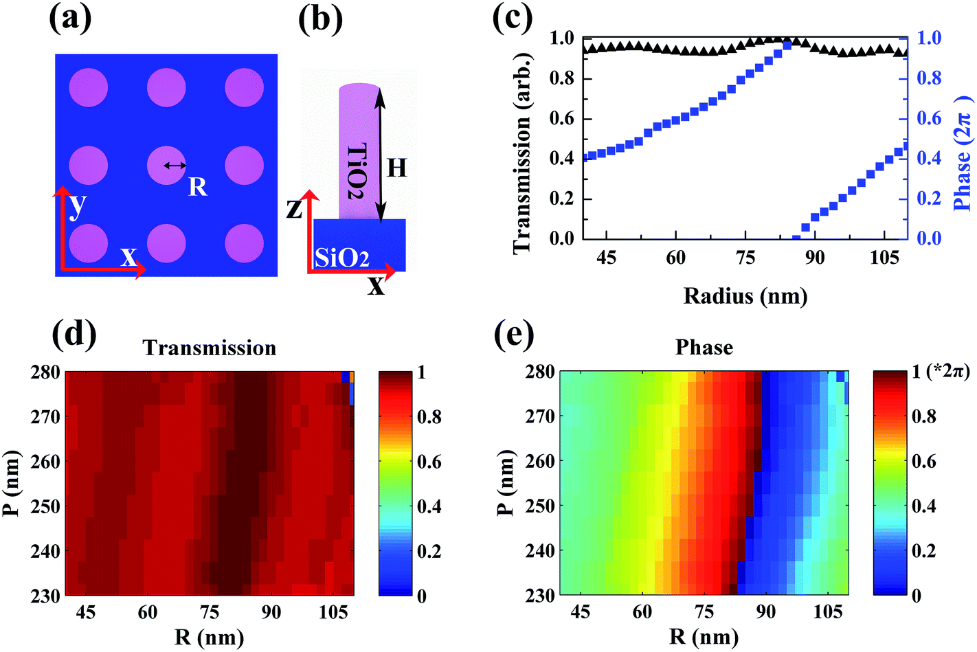 | ||
| Fig. 1 Schematic structure of metasurface with periodic TiO2 nanodisks (H = 650 nm, R = 80 nm, P = 245 nm). (a) Top view. (b) Side view. (c) Numerically calculated transmission (black triangle) and phase shift (blue square) for metasurfaces with varied radius and fixed period P = 245 nm at wavelength λ = 560 nm. Transmittance and transmitted light phase variation as a function of TiO2 nanodisk radius (R) and period (P) are shown in (d) and (e), respectively. | ||
To effectively manipulate the electromagnetic waves, simultaneous full 2π phase coverage and high transmittance are necessary. In our model, the phase modulation is achieved by means of the waveguiding effect caused by dielectric metasurface. Each nanodisk is considered as a waveguide and introduces a polarization-insensitive phase shift on the transmitted light. As shown in Fig. 1(d) and (e), with normally incident circular polarized illumination, the transmittance and corresponding phase as a function of radius and period of TiO2 nanodisks are clearly illustrated. Clearly, the phase of the light transmitted from the TiO2 nanodisk metasurfaces can span the entire 2π range. Without any significant resonance, the transmission amplitudes show almost uniform high values. This provides the high tolerance of metasurface hologram to fabrication error. For conventional electron beam lithography or reactive ion etching, all the meta-cells' sizes are increased or decreased with the same value for the fabrication error, which have no influence on the phase gradient. To design a high efficiency metasurface hologram, a number of meta-cells with fixed period of 245 nm are calculated, as shown in Fig. 1(c). When radius varies from 40 nm to 110 nm at a 2 nm interval, 2π phase range is achieved. With a pixel dimension of 245 nm, the metasurface hologram is sampled at less than half a wavelength, satisfying the Shannon–Nyquist sampling theorem.
To reproduce our institute's logo ‘SITP’, a 34-phase level computer-generated metasurface hologram was encoded to have it interfere with the normally incident circular polarized light at a wavelength of 560 nm. The working mechanism of our metasurface is shown in Fig. 2. According to the classical Gerchberg–Saxton algorithm, a 256 bit grayscale phase distribution of computer-generated hologram was obtained, as shown in Fig. 2(c). In order to effectively simplify the 256 bit hologram, we established an accurate relationship between the radius of the TiO2 nanodisks and phase shift, r = 44 × φ3 − 93 × φ2 + 117 × φ + 41, with data fitting in MATLAB. This equation provides a straightforward method to convert the phase configuration to radius arrangement. Finally, we chose the 34-phase level to reconstruct the metasurface based hologram. Due to the limitation of computer memory for simulations, the metasurface only consists of 200 × 200 evenly spaced TiO2 nanodisks. Radii varying from 42 nm to 108 nm at a 2 nm interval provide a precise phase control to ensure the high fidelity of far field imaging. Compared with conventional multistep lithography processes to fabricate 34-level phase hologram, our holographic metasurface only needs a single lithography step for the same.
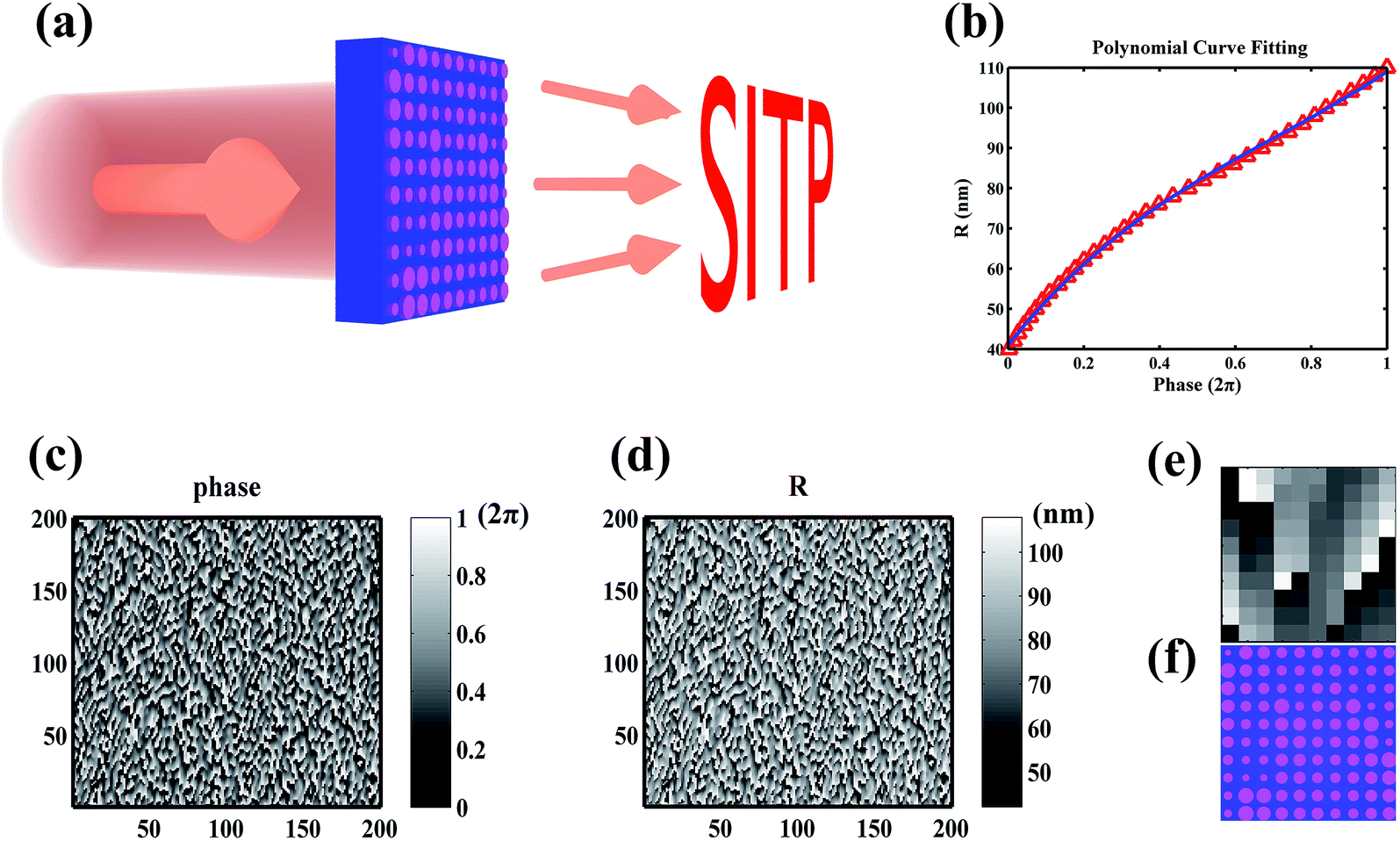 | ||
| Fig. 2 Design of the metasurface hologram. (a) Conceptual image ‘SITP’. (b) Polynomial curve fitting for the transmitted phase shift and radius of the TiO2 nanodisk. The red triangle and blue line represent the simulated result and the corresponding fitting curve, respectively. (c) The computer-generated grayscale phase distribution with 200 × 200 pixels designed to reconstruct the target holographic image, and (d) corresponding nanodisk radius distribution (200 × 200 meta-cells). (e) and (f) are the enlarged phase distribution (10 × 10 pixels) and its corresponding meta-cell distribution. | ||
Results and discussion
To characterize the performance of the metasurface-based hologram, far field intensity is calculated using the finite-difference time-domain (FDTD) method. Illuminated by normally incident plane wave with circular polarization, the target image is reproduced, as shown in Fig. 3(b) and (e). Even though only 200 × 200 meta-cells are adopted in this study, and the size of the metasurface (49 μm × 49 μm) is much smaller than the reported models,27,29 the target holographic image “SITP” and the enlarged “S” is clearly reproduced. It shows high fidelity with our metasurface hologram. More importantly, no twin image is observed in the simulated far field, which is due to the subwavelength meta-cell's diffraction. Only this one order diffraction property ensures the high imaging efficiency, which is in agreement with our previous result.31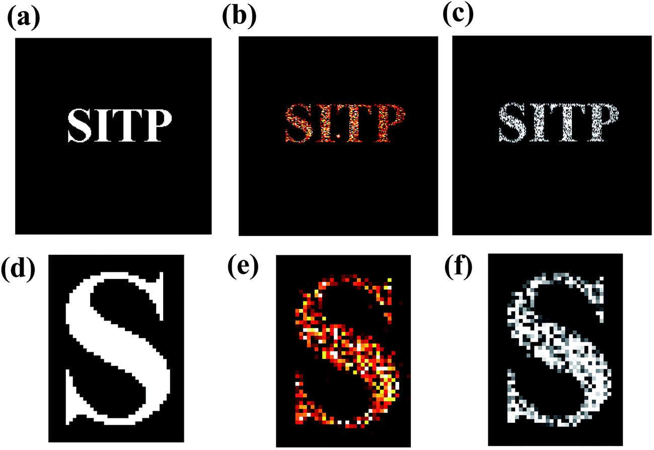 | ||
| Fig. 3 Image reproduction with a 34-phase level metasurface hologram. (a) The target image ‘SITP’. (b) Simulated holographic image acquired by the FDTD method. The far field intensity is normalized. (c) The selected effective pixels used to calculate the imaging efficiency. (d), (e), and (f) show the enlarged letter ‘S’ in (a), (b), and (c), respectively. | ||
To quantitatively evaluate the imaging property of the hologram, we first defined the transmittance efficiency as the ratio of far field intensity going through the metasurface to that passing through the same silica substrate without the TiO2 nanodisk array. Transmission efficiency of 78.15% was achieved. In addition, we selected the effective pixels from the simulated holographic image by image identification, as shown in Fig. 3(c) and (f). The conversion efficiency was calculated as the fraction of the total transmitted far field intensity passing through the selected effective area. Herein, 76.41% of the transmitted far field intensity was converted into the hologram image. Furthermore, we defined the imaging efficiency as the product of transmission efficiency and conversion efficiency. With 59.72% imaging efficiency of the phase-only hologram, our hologram possesses the highest imaging efficiency on comparison with other polarization-insensitive metasurface based holograms.28–30 Moreover, the imaging efficiency can be further enhanced through the addition of more meta-cells or by increasing phase levels.
In addition to the high fidelity and high imaging efficiency, other imaging characteristics such as broadband, wide-angle, and high fabrication tolerance are also investigated to characterize our metasurface hologram. To check the broadband property, far field imaging is calculated for circular polarized incidence at wavelengths of 450 nm, 480 nm, 514 nm, 553 nm, 600 nm, 654 nm, as shown in Fig. 4. The intensity distributions clearly illustrate the target holographic image. This demonstrates the excellent broadband property of the metasurface hologram. Essentially, this phenomenon is due to the non-resonant nature of the meta-cells. We also notice that the sizes of the holographic images are enlarged with increasing wavelength. We attribute this to the change of phase accumulation during the propagation, as demonstrated in ref. 25.
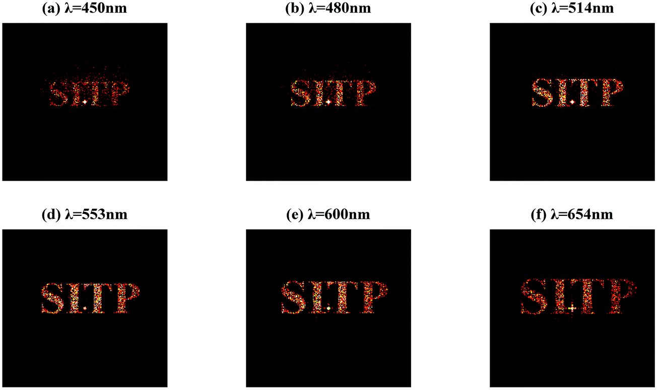 | ||
| Fig. 4 Broadband property of the hologram. Far field intensity images simulated at the wavelength of (a) 450 nm, (b) 480 nm, (c) 514 nm, (d) 553 nm, (e) 600 nm, (f) 654 nm. | ||
The wide-angle imaging property is also demonstrated with FDTD simulations. As shown in Fig. 5, the far field intensities are calculated for oblique incidence at 560 nm wavelength. With incident angles θi = 5°, 10°, 15°, 20°, 25°, the zeroth-order beams focus at spots with deviation angles θ = 8°, 15°, 23°, 31°, 38° respectively. With 76.41%, 72.69%, 67.65%, 61.93%, 55.98% transmittance efficiency, the target holographic image is reconstructed clearly at the five incident angles except the blurry “P” at θi = 25°. The wide-angle imaging property is because of the selected non-resonance TiO2 nanodisks, which are insensitive to oblique incidence. Herein, we want to emphasize that our metasurface-based hologram not only has no polarization dependence on the reference beam, but also lowers the collimation demand of incidence light.
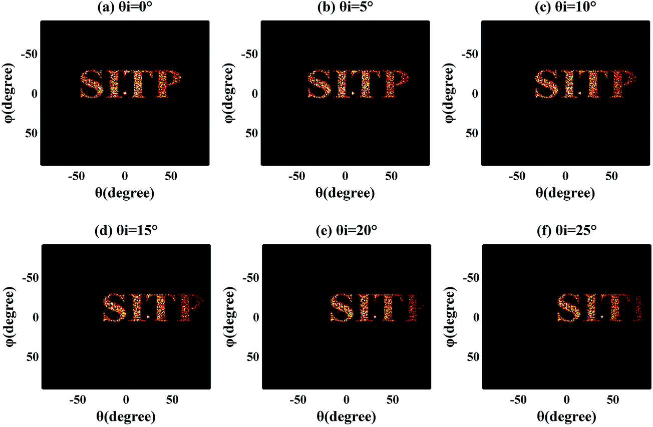 | ||
| Fig. 5 Imaging dependence on the incidence angle. Far field intensities for the metasurface hologram simulated with incident angle (a) 0°, (b) 5°, (c) 10°, (d) 15°, (e) 20°, (f) 25°, at designed wavelength. | ||
To promote the application of metasurface in large-scale holographic technology, keeping a large fabrication tolerance is important to ensure the performance of the fabricated device. In this study, uniform and random dimension errors caused by the electron beam lithography or reactive ion etching are both considered, as shown in Fig. 6. With 62%, 61.6%, 51.9%, 57.23% imaging efficiency, the holographic images are represented without any significant degradation of the performance, as shown in Fig. 6. In this case, due to the approximate linear relationship of radius and phase shift, the phase gradient can be seen as a constant, which ensures the high imaging efficiency. This promises that our polarization-insensitive meta-hologram has a very good tolerance to the fabrication error.
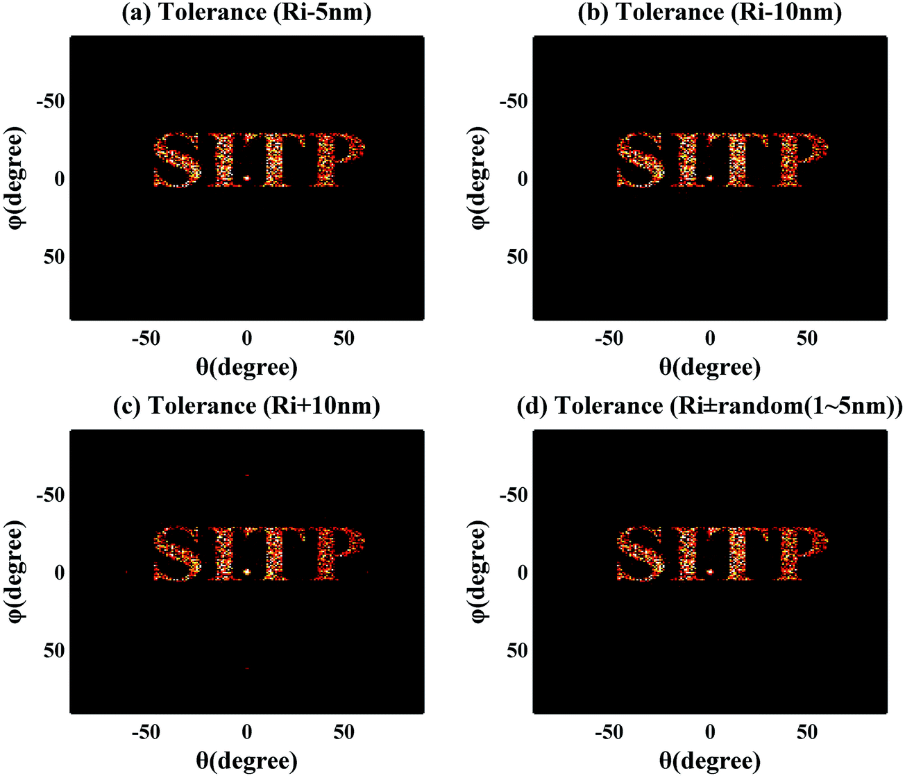 | ||
| Fig. 6 High tolerance to fabrication errors. Simulated far field intensities for metasurface with different nanodisks. All nanodisks' radii with (a) minus 5 nm, (b) minus 10 nm, (c) plus 10 nm at designed Ri. (d) Every nanodisk adds a random error (±1–5 nm). | ||
Conclusion
In conclusion, we proposed a metasurface of 34-phase level based hologram in the visible range. With high fidelity, the micrometer-scale metasurface hologram can achieve an imaging efficiency as high as 59.72% at 560 nm wavelength. In addition, we also demonstrated the imaging properties with broadband, wide-angle, and high fabrication tolerance for the metasurface hologram. With such excellent performance, the dielectric metasurface can be used in holographic display, high resolution holographic data storage, optical information processing etc.Acknowledgements
The authors acknowledge the support provided by the State Key Program for Basic Research of China (2013CB632705, 2011CB922004), the National Natural Science Foundation of China (10990104, 11334008, and 61290301), the Fund of Shanghai Science and Technology Foundation (13JC1408800, 16ZR1445300), Shanghai Sailing Program (16YF1413200), and Youth Innovation Promotion Association CAS (2017285).References
- R. A. Shelby, D. R. Smith and S. Schultz, Science, 2001, 292(5514), 77–79 CrossRef CAS PubMed.
- C. M. Soukoulis, S. Linden and M. Wegener, Science, 2007, 315(5808), 47–49 CrossRef CAS PubMed.
- D. Ye, K. Chang, L. Ran and H. Xin, Nat. Commun., 2014, 5, 5841 CrossRef CAS PubMed.
- S. Xi, H. Chen, T. Jiang, L. Ran, J. Huangfu, B. I. Wu, J. A. Kong and M. Chen, Phys. Rev. Lett., 2009, 103, 194801 CrossRef PubMed.
- S. N. Galyamin, A. V. Tyukhtin, A. Kanareykin and P. Schoessow, Phys. Rev. Lett., 2009, 103, 194802 CrossRef PubMed.
- P. Genevet, D. Wintz, A. Ambrosio, A. She, R. Blanchard and F. Capasso, Nat. Nanotechnol., 2015, 10(9), 804–809 CrossRef CAS PubMed.
- S. H. Lee, C. M. Park, Y. M. Seo and C. K. Kim, Reversed Doppler effect in double negative metamaterials, Phys. Rev. B: Condens. Matter Mater. Phys., 2010, 81, 241102 CrossRef.
- D. Ziemkiewicz and S. Zielinska-Raczynska, J. Opt. Soc. Am. B, 2015, 32(3), 363–369 CrossRef CAS.
- J. Ran, Y. Zhang, X. Chen, K. Fang, J. Zhao, Y. Sun and H. Chen, Sci. Rep., 2015, 5, 11659 CrossRef CAS PubMed.
- N. Yu, P. Genevet, M. A. Kats, F. Aieta, J. P. Tetienne, F. Capasso and Z. Gaburro, Science, 2011, 334(6054), 333–337 CrossRef CAS PubMed.
- L. Huang, X. Chen, H. Mühlenbernd, G. Li, B. Bai, Q. Tan, G. Jin, T. Zentgraf and S. Zhang, Nano Lett., 2012, 12(11), 5750–5755 CrossRef CAS PubMed.
- Y. Yang, W. Wang, P. Moitra, I. I. Kravchenko, D. P. Briggs and J. Valentine, Nano Lett., 2014, 14(3), 1394–1399 CrossRef CAS PubMed.
- X. Ma, M. Pu, X. Li, C. Huang, Y. Wang, W. Pan, B. Zhao, J. Cui, C. Wang, Z. Zhao and X. Luo, Sci. Rep., 2015, 5, 10365 CrossRef CAS PubMed.
- X. Chen, L. Huang, H. Mühlenbernd, G. Li, B. Bai, Q. Tan, G. Jin, C. Qiu, S. Zhang and T. Zentgraf, Nat. Commun., 2012, 3, 1198 CrossRef PubMed.
- F. Aieta, P. Genevet, M. A. Kats, N. Yu, R. Blanchard, Z. Gaburro and F. Capasso, Nano Lett., 2012, 12(9), 4932–4936 CrossRef CAS PubMed.
- X. Ni, S. Ishii, A. V. Kildishev and V. M. Shalaev, Light: Sci. Appl., 2013, 2(4), e72 CrossRef.
- D. Lin, P. Fan, E. Hasman and M. L. Brongersma, Science, 2014, 345(6194), 298–302 CrossRef CAS PubMed.
- A. Arbabi, Y. Horie, M. Bagheri and A. Faraon, Nat. Nanotechnol., 2015, 10, 937–943 CrossRef CAS PubMed.
- M. Khorasaninejad, A. Y. Zhu, C. Roques-Carmes, W. T. Chen, J. Oh, I. Mishra, R. C. Devlin and F. Capasso, Nano Lett., 2016, 16(11), 7229–7234 CrossRef CAS PubMed.
- N. Yu, F. Aieta, P. Genevet, M. A. Kats, Z. Gaburro and F. Capasso, Nano Lett., 2012, 12(12), 6328–6333 CrossRef CAS PubMed.
- Z. H. Jiang, L. Lin, D. Ma, S. Yun, D. H. Werner, Z. Liu and T. S. Mayer, Sci. Rep., 2014, 4, 7511 CrossRef CAS PubMed.
- F. Ding, Z. Wang, S. He, V. M. Shalaev and A. V. Kildishev, ACS Nano, 2015, 9(4), 4111–4119 CrossRef CAS PubMed.
- B. Wang, F. Dong, Q. T. Li, D. Yang, C. Sun, J. Chen, Z. Song, L. Xu, W. Chu, Y. F. Xiao, Q. Gong and Y. Li, Nano Lett., 2016, 16(8), 5235–5240 CrossRef CAS PubMed.
- E. Almeida, O. Bitton and Y. Prior, Nat. Commun., 2016, 7, 12533 CrossRef CAS PubMed.
- L. Huang, X. Chen, H. Mühlenbernd, H. Zhang, S. Chen, B. Bai, Q. Tan, G. Jin, K. W. Cheah, C. W. Qiu, J. Li, T. Zentgraf and S. Zhang, Nat. Commun., 2013, 4, 2808 Search PubMed.
- X. Ni, A. V. Kildishev and V. M. Shalaev, Nat. Commun., 2013, 4, 2807 Search PubMed.
- G. Zheng, H. Mühlenbernd, M. Kenney, G. Li, T. Zentgraf and S. Zhang, Nat. Nanotechnol., 2015, 10(4), 308–312 CrossRef CAS PubMed.
- Q. T. Li, F. Dong, B. Wang, F. Gan, J. Chen, Z. Song, L. Xu, W. Chu, Y. F. Xiao, Q. Gong and Y. Li, Opt. Express, 2016, 24(15), 16309–16319 CrossRef PubMed.
- K. E. Chong, L. Wang, I. Staude, A. R. James, J. Dominguez, S. Liu, G. S. Subramania, M. Decker, D. N. Neshev, I. Brener and Y. S. Kivshar, ACS Photonics, 2016, 3(4), 514–519 CrossRef CAS.
- W. Zhao, H. Jiang, B. Liu, J. Song, Y. Jiang, C. Tang and J. Li, Sci. Rep., 2016, 6, 30613 CrossRef CAS PubMed.
- G. Li, B. P. Clarke, J. K. So, K. F. MacDonald and N. I. Zheludev, Nat. Commun., 2016, 7, 13705 CrossRef CAS PubMed.
| This journal is © The Royal Society of Chemistry 2017 |