
 Open Access Article
 This Open Access Article is licensed under a
 Creative Commons Attribution 3.0 Unported Licence
InGaN/GaN nanowires epitaxy on large-area MoS2 for high-performance light-emitters†
Chao Zhao a,
Tien Khee Nga,
Chien-Chih Tsengb,
Jun Lib,
Yumeng Shib,
Nini Weid,
Daliang Zhangd,
Giuseppe Bernardo Consiglioa,
Aditya Prabaswaraa,
Abdullah Ali Alhamouda,
Abdulrahman M. Albadric,
Ahmed Y. Alyamanic,
X. X. Zhangb,
Lain-Jong Lib and
Boon S. Ooi*a
a,
Tien Khee Nga,
Chien-Chih Tsengb,
Jun Lib,
Yumeng Shib,
Nini Weid,
Daliang Zhangd,
Giuseppe Bernardo Consiglioa,
Aditya Prabaswaraa,
Abdullah Ali Alhamouda,
Abdulrahman M. Albadric,
Ahmed Y. Alyamanic,
X. X. Zhangb,
Lain-Jong Lib and
Boon S. Ooi*a
aKing Abdullah University of Science and Technology (KAUST), Photonics Laboratory, Thuwal 23955-6900, Saudi Arabia. E-mail: boon.ooi@kaust.edu.sa
bKing Abdullah University of Science and Technology (KAUST), Physical Sciences and Engineering Division, Thuwal 23955-6900, Saudi Arabia
cKing Abdulaziz City for Science and Technology (KACST), National Center for Nanotechnology, Riyadh 11442-6086, Saudi Arabia
dKing Abdullah University of Science and Technology (KAUST), Imaging and Characterization Core Lab, Thuwal 23955-6900, Saudi Arabia
First published on 18th May 2017
Abstract
The recent study of a wide range of layered transition metal dichalcogenides (TMDCs) has created a new era for device design and applications. In particular, the concept of van der Waals epitaxy (vdWE) utilizing layered TMDCs has the potential to broaden the family of epitaxial growth techniques beyond the conventional methods. We report herein, for the first time, the monolithic high-power, droop-free, and wavelength tunable InGaN/GaN nanowire light-emitting diodes (NW-LEDs) on large-area MoS2 layers formed by sulfurizing entire Mo substrates. MoS2 serves as both a buffer layer for high-quality GaN nanowires growth and a sacrificial layer for epitaxy lift-off. The LEDs obtained on nitridated MoS2 via quasi vdWE show a low turn-on voltage of ∼2 V and light output power up to 1.5 mW emitting beyond the “green gap”, without an efficiency droop up to the current injection of 1 A (400 A cm−2), by virtue of high thermal and electrical conductivities of the metal substrates. The discovery of the nitride/layered TMDCs/metal heterostructure platform also ushers in the unparalleled opportunities of simultaneous high-quality nitrides growth for high-performance devices, ultralow-profile optoelectronics, energy harvesting, as well as substrate reusability for practical applications.
Introduction
Nitride materials have been considered one of the most important semiconductors after silicon because of their versatile properties in applications such as solid-state lighting (SSL), energy harvesting, sensing, dermatology, and single-photon emission.1–5 However, the quality of the materials grown on conventional sapphire substrates limits their development. In recent years, nitride nanowires and nanorods have attracted much attention due to their various advantages over planar nitride thin films, such as the possibility of growth on dissimilar substrates with nearly zero dislocation, reduced strain through radial relaxation, and improved light extraction.6 Nitride nanowires showed the potential to overcome various obstacles in SSL, such as the quantum-confined Stark effect (QCSE) induced degradation in device performance, the “green gap”, and efficiency droop.7 In this regard, nitride nanowire light-emitting diodes (NW-LEDs) and lasers on Si emitting from green to near-infrared have been demonstrated.8–11 Moreover, nitride nanowires and devices have also been reported on bulk transition metal substrates or transition metal thin films to further address the electrical- and thermal-conductivities issues.12–15It is noted that the transition metal substrates such as Mo have also been used for the large-scale synthesis of transition metal dichalcogenides (TMDCs),16–18 which are candidates as components of electronic and optoelectronic devices due to their inherent optical and electronic properties.19–21 TMDCs has been reported as an integral part of the p–n junction.22 Recently, researchers have also shifted their focus from studying the TMDCs materials themselves to the application of TMDCs in various fields. Because of the small lattice mismatch with III-nitrides, TMDCs have been considered novel substrates or surfaces for nitride growth. Akiyoshi Yamada et al. reported GaN thin film growth on bulk MoS2 using molecular beam epitaxy (MBE);23 Priti Gupta et al. also demonstrated GaN crystals obtained on MoS2 flakes using metal organic chemical vapor deposition (MOCVD).24 Furthermore, it is possible to grow an epilayer on TMDCs via quasi van der Waals epitaxy (vdWE) without satisfying lattice match between them, which is a common dislocation-free crystal growth method in recent years.25–32 Jeehwan Kim et al. reported growth of high-quality GaAs(001) on graphene–GaAs substrates.33 In the meantime, since layered TMDCs can act as sacrificial layers for lifting-off devices from substrates, it will enable the substrates to be reused for multiple epitaxy growths.34,35 Although GaN thin film and nanowires growth on other layered materials such as boron nitride (BN), graphite, and graphene has also been reported; the methods were not favorable for device applications, or the devices have limited performance.36–40 Moreover, the mechanism of nitride growth on layered materials remains unexplored because of the limited material quality of nitride or its relatively high growth temperature, which is detrimental to TMDCs. Until now, no nitride nanowire or device on TMDCs, especially large-area TMDCs, has been developed. Essentially, large-scale, high-quality material growth on commercial substrates and the ability to lift-off epilayer to reuse the substrates are necessary to open up new opportunities for nitride nanowires and devices in practical applications.
Here, for the first time, we demonstrate the monolithic high-quality InGaN/GaN quantum-disks (Qdisks)-in-nanowire LEDs with tunable emission in the visible region on large-area MoS2/Mo. By sulfurizing the entire commercial Mo substrate using chemical vapor deposition (CVD), large-scale multiple MoS2 layers were formed. Because of the relatively low growth temperature of GaN by MBE compared to that of MOCVD, the integrity of the MoS2 layers was preserved.24 The growth was confirmed proceed through the nitridation of MoS2 by nitrogen plasma using X-ray diffraction (XRD) and transmission electron microscopy (TEM). By optimizing the growth conditions, the GaN crystalline quality obtained via quasi vdWE is comparable to that found in existing reports, despite the lattice mismatch between the Mo2N and GaN. Furthermore, the better optical quality of GaN and internal quantum efficiency (IQE) of 62.4% for these Qdisks accentuate the benefits of the MoS2 layer. NW-LEDs thus produced show a low turn-on voltage of ∼2 V and light output power up to 1.5 mW emitting beyond the “green gap”, without an efficiency droop up to the current injection of 1 A (400 A cm−2), by virtue of high thermal and electrical conductivities of the metal substrates. We further demonstrated the release of the entire GaN nanowires-epitaxy from the Mo substrates. Thus the layered TMDCs/metal platform not only enables the growth of nitrides for high-power devices but also allows potential recycle of Mo substrate for cost efficiency. Moreover, the unprecedented opportunities to integrate nitride/layered TMDCs/metal in this platform can surpass the conventional limitation in heterogeneous integration. The high-vacuum and oxygen-free environment also begins a new era for MoS2 processing using MBE.41 By combining CVD and MBE as a cluster tool, low cost, monolithic nitride material and devices on large-area MoS2 and other layered TMDCs can be promising for multidisciplinary applications, such as SSL, energy harvesting, visible-light communications, bio-sensing, and lasers.
Experimental
Before loading into the MBE chamber, commercial polycrystalline Mo substrates with dimensions of 1 cm × 1 cm × 0.05 cm were sulfurized by placing them at the center of a 1 inch hot-wall CVD furnace. Sulfur powders were placed in a ceramic boat at the upstream side and kept at 320 °C during the reaction. The furnace was then pumped to a background pressure of ∼5 mTorr, followed by introducing a flowing gas mixture consisting of Ar at 100 standard cubic centimeters per minute (sccm) and H2 at 20 sccm to reach an ambient pressure. Next, the furnace was heated to 1050 °C at a ramping rate of 25 °C min−1. The heating zone was maintained at that temperature for 1 hour and then rapidly cooled to room temperature (RT) at a cooling rate of 3 °C s−1. The nanowires were then grown on the sulfurized Mo substrates using a Veeco Gen 930 plasma-assisted MBE system as described in our previous reports.14,42 The substrate temperature was monitored using a pyrometer. The NW-LEDs were composed of 150 nm-thick Si-doped n-type GaN grown at 660 °C and the active region of 8 pairs of InGaN-disk (∼3 nm)/GaN-barrier (∼12 nm), which were grown at different conditions to tune the emission wavelength. The Mg-doped p-GaN (∼50 nm) was grown at a substrate temperature of 570 °C. The plasma source was operated at 400 W using a constant N2 flow rate of 1.5 sccm.The surface morphologies of the substrates before and after MBE growth were characterized using both an optical microscope (OM) and an FEI Magellan FEG field-emission scanning electron microscope (FE-SEM). After growth, the crystal quality and the orientation of nanowires were examined using a Bruker D8 Discover XRD with a Cu Kα source. To study the growth mechanism by characterizing the interface between the nanowires and the sulfurized Mo, we prepared a cross-sectional TEM sample using an in situ lift-out technique in an FEI Helios NanoLab 400s-focused ion beam (FIB)/SEM. High-angle annular dark field (HAADF) scanning transmission electron microscopy (STEM) images were taken using an FEI probe-corrected Titan at an acceleration voltage of 300 kV. Raman spectra of GaN and MoS2 were measured on a Horiba Jobin Yvon confocal micro-Raman system using 473 nm laser excitation in the backscattering geometry. Temperature-dependent photoluminescence (TDPL) measurements were performed using a 405 nm excitation cw laser from 10 to 300 K to reveal the emission wavelength of the Qdisks and to calculate the IQE. We also tested the power–current–voltage (L–I–V) characteristics of the fabricated NW-LEDs using a microscope-based electroluminescence (EL) system.14,42 To lift-off the nanowire epitaxy on the substrate, the sample was coated with poly(methyl methacrylate) (PMMA) and baked at a temperature of 180 °C for 60 s to protect the epitaxy from xenon difluoride (XeF2) exposure. The edge of the sample was then cleaned to expose to XeF2 gas, followed by being etched at 4 Torr for 30 s and repeated 100 cycles.
Results and discussion
The sulfurization process of Mo substrates was optimized to ensure a relatively smooth surface for the subsequent nanowire growth (see the ESI† for more details on the sulfurization of Mo substrates, S1). To verify its stability in ultra-high vacuum, the MoS2/Mo substrate was heated to 700 °C in the growth chamber, which is the typical GaN growth condition in our MBE and lower than the growth temperature of GaN on Si because of the difference in substrates and other growth conditions.43 Fig. 1(a) shows the OM image of the MoS2 layer with grain boundaries, which appears similar to the surface before heat treatment (see Fig. S1(c) in the ESI,† S1). The Raman spectra (see Fig. S1(b)†) of the substrates before and after the heat treatment show the E12g and A1g phonon modes at 384.0 ± 0.5 and 408.0 ± 0.5 cm−1 corresponding to the in-plane vibration of Mo and S atoms and the out-of-plane vibration of only S atoms in bulk MoS2, respectively.44 Due to the lower GaN growth temperature of MBE than that of MOCVD, MoS2 is stable and thus a suitable buffer layer for subsequent growth.24 Fig. 1(c) and (d) show SEM images of vertical nanowires with a hexagonal shape and nonpolar sidewall facets after the growth at a substrate temperature of 700 °C with a Ga beam equivalent pressure of 2.5 × 10⁻⁸ Torr for 2 hours on MoS2/Mo, although parasitic islands growth persists because of the rough surface of the substrates. Without MoS2, only polycrystalline GaN island growth occurs on the surface of the Mo substrates under the same growth conditions (see the ESI for more details on the growth of GaN on Mo and MoS2/Mo,† S2), thus confirming that the growth of GaN nanowires is selective to the sulfurized Mo surface, which is consistent with other reports.24 The nanowires have an average diameter of 20–55 nm, an average length of ∼130 nm, and a density of 2.6 × 1010 cm−2 which can be further increased by tuning the growth conditions.14 The parasitic growth can be suppressed by using smoother Mo substrates and improving the sulfurization process.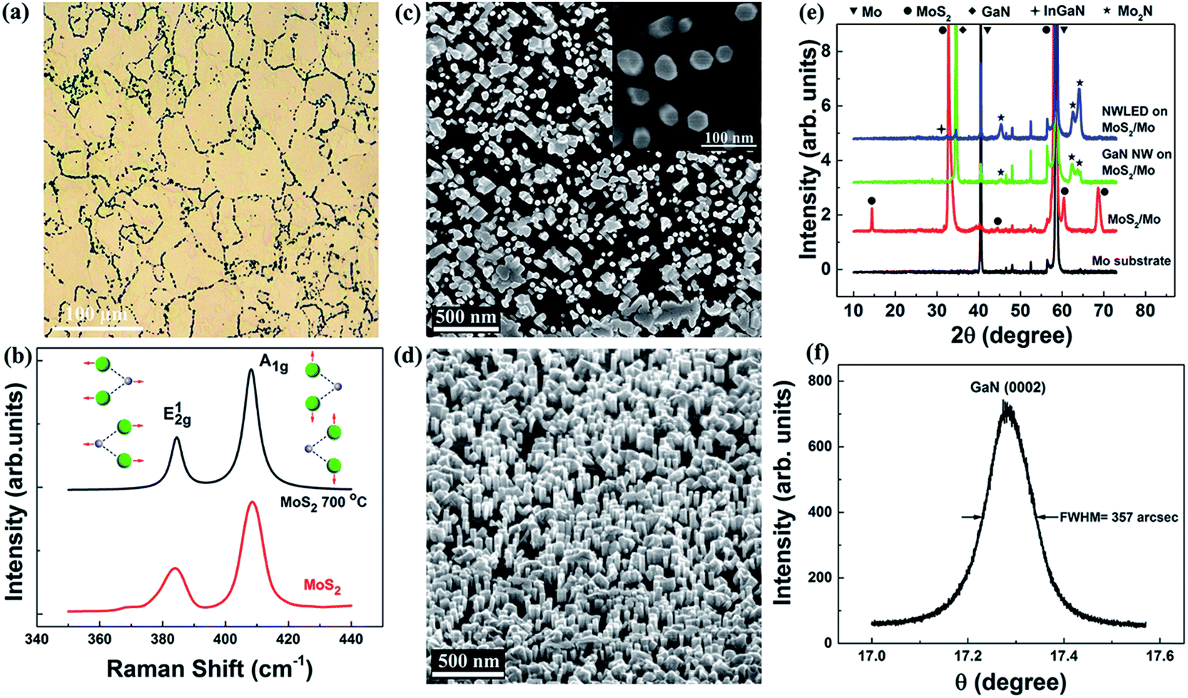 | ||
| Fig. 1 (a) The OM image for MoS2/Mo at 700 °C, which is the typical GaN growth temperature in MBE; (b) Raman spectra of MoS2 with Stokes line in a backscattering configuration; the insets depict phonon modes of MoS2. Atom color code: grey, Mo; green, S; (c) plan-view and (d) elevation-view SEM images of the GaN nanowires grown on MoS2/Mo substrates, the inset of (c) shows the high magnification SEM images of nanowires with hexagonal shape; (e) the XRD curves of the samples; and (f) rocking curve of GaN(0002) planes. | ||
The XRD results of the Mo substrate, sulfurized Mo substrate, GaN nanowires grown on MoS2/Mo, and InGaN/GaN Qdisks-in-nanowires grown on MoS2/Mo are shown in Fig. 1(e). Mo(110) and (200) peaks were observed in the polycrystalline Mo substrate (Joint Committee on Powder Diffraction Standards (JCPDS) card no. 004-0809). After sulfurization, (002), (100), (006), (110), (008), and (200) peaks of polycrystalline MoS2 appeared (JCPDS card no. 037-1492), confirming the surface sulfurization of the Mo substrates. With GaN growth, the MoS2 peaks disappeared, and instead, Mo2N(004), (220), and (204) peaks and GaN(0002) peak formed (JCPDS card no. 25-1368 and 50-0792), which indicates the formation of a polycrystalline Mo2N layer before the single-crystal nanowire growth. It has been reported that MoS2 can be doped with nitrogen and Mo–N bonds can form using remote N2 plasma.45 In our growth condition, the MoS2 layer was nitridated by the nitrogen radicals before the nanowire formation, which cannot be avoided using the growth conditions reported herewith. The full-width at half-maximum (fwhm) value from the GaN(0002) rocking curve (θ scan) of the nanowires (see Fig. 1(f)) was 357 arcsec, which is smaller than those reported for GaN nanowires grown on other substrates.14 This result is due to the high crystalline quality of the vertically aligned nanowires when grown on MoS2/Mo, although they are randomly oriented in-plane. The InGaN(0002) reflection of InGaN/GaN Qdisks-in-nanowires was also observed, which can be used to estimate the In composition in the Qdisks, assuming the relaxation of InGaN and ignoring the Poisson ratio.
The optical and structural properties of GaN nanowires and InGaN/GaN Qdisks in nanowires grown on MoS2/Mo were further examined by microphotoluminescence (µPL) and Raman spectroscopy. Fig. 2(a) shows the PL spectra of GaN grown on the MoS2/Mo and Mo (see Fig. 1(c) and S2(a) in the ESI, S2; Fig. S3 in the ESI,† S3). The band-to-band optical transition of GaN nanowires at 365 nm was observed when growing on both Mo and MoS2/Mo. However, the GaN grown on Mo showed defect-related emission at approximately 380 nm and deep-level transition at 500 nm due to the absence of MoS2,46–48 which would severely degrade the device performance by creating a secondary recombination path.49 We further compared the quality of the GaN using Raman spectroscopy. Fig. 2(b) also shows the Raman spectra of the nanowires measured in the backscattering configuration using a 473 nm laser excitation. The E2 high-frequency mode E2(high) at 565 cm−1 and longitudinal optical (LO) phonon mode A1(LO) at 733 cm−1 were observed, which were attributed to hexagonal GaN.50 The first-order transverse optical (TO) phonon mode A1(TO) at 534 cm−1 was also observed for GaN grown on Mo. In the current backscattering configuration, the TO phonon mode was supposed to be forbidden according to the Raman selection rules in the wurtzite crystal of GaN, which were weakened because of the defects when grown on Mo.51,52 Thus, the GaN grown on MoS2/Mo showed higher material quality. Moreover, InGaN/GaN Qdisks-in-nanowires emitting at 515 nm were also grown on MoS2/Mo. TDPL measurements were performed to evaluate the IQE of these Qdisks, which was estimated to be 62.4% using the ratio of the integrated PL intensity at 300 K to that at 10 K as shown in Fig. 2(c), assuming the nonradiative recombination centers are frozen at 10 K.53 The blue shift in Fig. 2(c) is due to the temperature-dependent increase in the bandgaps.54 Power dependent photoluminescence spectra for these InGaN/GaN Qdisks-in-nanowires are shown in Fig. 2(d). Evidently, no peak emission blue shifted with increasing excitation power, which confirms the negligible piezoelectric field and related QCSE due to the lateral strain relaxation.55,56
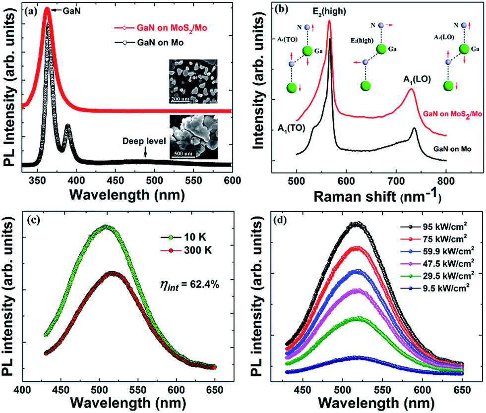 | ||
| Fig. 2 (a) RT PL for GaN grown on MoS2/Mo and Mo, respectively; the insets show plan-view SEM images of GaN; (b) Raman spectra of GaN with Stokes lines in a backscattering configuration; the insets depict the phonon modes of GaN. Atom color code: grey, N; green, Ga; (c) TDPL of Qdisks at 10 and 300 K, excited using a 405 nm laser; (d) power dependent PL of Qdisks at RT. | ||
We also characterized the nanowires/substrate interface using cross-sectional TEM to study the role of the MoS2 layer in the growth of GaN nanowires on MoS2/Mo. The SEM image (see Fig. 3(a) and S4(b) in the ESI,† S4) of the TEM sample prepared by FIB clearly shows the Mo grains of polycrystalline Mo substrates, on top of which are the 60 nm buffer layer, and vertical nanowires (see the ESI† for more details on the FIB-TEM of GaN on MoS2/Mo, S4). The inset of Fig. 3(a) shows the selected area electron diffraction (SAED) pattern obtained from the [2−1−10] zone axis of the GaN nanowires in TEM, which were single crystalline and exhibited a preferred orientation of [0002]. Fig. 3(b) and S4(c)† show the HAADF-STEM image of nanowires taken along the same zone axis, in which no obvious defect was found even at the roots of the nanowires. Fig. 3(c) and S4(d)† show the high-resolution (HR) HAADF-STEM images with a clear atomic arrangement of the GaN nanowire and the buffer layer below; the measured lattice spacing of ∼5.2 Å parallel to the long axis of the nanowire is in good agreement with the reported value for wurtzite GaN crystal (c axis), thus further confirming the [0002] growth direction of the nanowires. The GaN nanowire/buffer layer interface is coherent and sharp; the GaN nanowire is nearly free of defects. Fig. 3(d) shows the electron energy loss spectroscopy (EELS) elemental maps of Ga, Mo, and N across the interface, which confirmed that GaN nanowires were grown on the Mo2N buffer layer. The measured lattice spacing of ∼4.2 Å for the buffer layer is in good agreement with the known d-spacing value of tetragonal Mo2N crystal along [100] (see Fig. S4(d) in the ESI,† S4). From XRD and TEM results, the MoS2 layer with a thickness of 60 nm was completely nitrided to Mo2N buffer layer before nanowires growth. The weak quasi van der Waals interaction was believed to exist between GaN and Mo2N, thus ensuring the high-quality GaN formation in spite of the large lattice mismatch between them.28–30 Since the nitridation of Mo is more difficult than MoS2, there is a selective growth of GaN on MoS2.45,57 The polycrystallization of the Mo2N layer affected the growth front and the nucleation, thus the orientation of GaN nanowires.
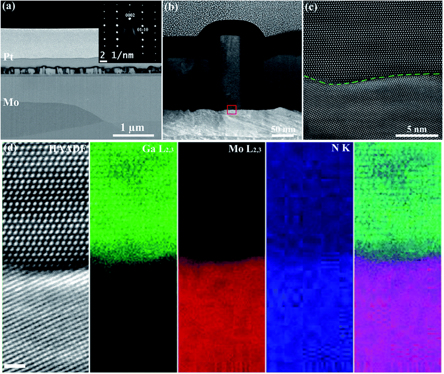 | ||
| Fig. 3 (a) The SEM image of the FIB sample; (b) the STEM image of nanowires on MoS2/Mo substrates; (c) HR HAADF-STEM image of the atomically sharp interface between the nanowires and substrates in the red square area in (b), which is highlighted by the green dashed lines; (d) HAADF-STEM image, false-color Ga, Mo and N elemental concentration maps of the interface, and a combined elemental map with Ga in green, Mo in red and N in blue. The scale bar is 1 nm. | ||
To further demonstrate the functionality of this layered TMDCs-based technique, we fabricated NW-LEDs with tunable emission in the visible region using these high-quality nitride material. Fig. 4(a) shows the L–I–V characteristics of a yellow NW-LED with dimensions of 500 µm × 500 µm on MoS2/Mo measured under dc injection. The inset of Fig. 4(a) shows SEM images of the high-density nanowires used for the LED. The LED has a low turn-on voltage of ∼2 V due to the existence of the Mo2N layer, which has been shown to possess metallic conductivity.58,59 In the continuous-wave mode, when operating at 1 A injection current and ∼5 V forward bias voltage, the light output power was up to 1.5 mW, which is relatively high in this wavelength region. The output power of LEDs can be further increased by increasing the nanowire density when growing on smooth Mo substrates. Fig. 4(b) shows the RT EL spectra of the NW-LEDs emitting at 470 and 635 nm when using different Qdisks growth conditions, which demonstrated the tunable emission wavelength beyond the “green gap”; the inset shows the charge-coupled device (CCD) images for the illuminated LEDs (see the ESI† for videos demonstrating the operation of the NW-LEDs). Fig. 4(c) shows the RT EL spectra of the yellow LED at different injection current densities, in which the LED emitted at ∼635 nm with a negligible blue shift in the injection current range of 300–1000 mA. The external quantum efficiency (EQE) of the NW-LED was calculated using the equation ηext = (P/hν)/(I/e), where P is the measured light output power by the power meter, h is Planck's constant, ν is the frequency of light from the EL spectra of the LED, I is the injection current for the LED, and e is the electron charge. The LED does not show efficiency droop up to the injection current of 1 A (400 A cm−2) at ∼5 V forward bias voltage, as shown in Fig. 4(d). It is possibly due to the high thermal and electrical-conductivities of the metal substrates.14,42 Further improvement of EQE can be realized by exfoliating the LED from the substrate as shown in the inset in Fig. 4(d), if the thermal conductivity can be addressed.
 | ||
| Fig. 4 (a) Typical L–I–V characteristics of the LED with dimensions of 500 µm × 500 µm on MoS2/Mo; (b) the EL spectra of the LEDs; the inset shows OM images of the illuminated blue and yellow LEDs; (c) the EL spectra of the LED at injection current from 300–1000 mA; (d) the EQE of LEDs with current density; the inset shows the schematic of the LED and potential improvement of EQE by releasing the LED from metal. | ||
Developing large-scale exfoliation processes with high reproducibility for epitaxy layers is especially important for device applications.60 Here, we further demonstrated a chemical exfoliation process that maintains the quality of the nanowire epitaxy by removing the layered TMDCs. The nitridation of MoS2 depends on the nitrogen plasma condition used in our process. Since both MoS2 and Mo2N can be etched using XeF2, the epitaxy can also be lifted-off even if the MoS2 layers partially remain after nanowire growth, which shows the flexibility of our process.35,61 Fig. 5(a) shows an OM image of the sample after the nanowire growth, in which grain boundary features remained. Fig. 5(a1) shows the Raman spectra of the sample at different regions, which clearly exhibit the features of MoS2. The PL spectrum in Fig. 5(a2) shows the GaN band-edge emission at 365 nm, confirming the formation of GaN nanowires. After etching using XeF2 at RT,62 the nanowires and boundary features on the GaN nanowire membranes were similar to those observed on the surface of the sample before etching, as shown in Fig. 5(b) and (c), implying the precise removal of the entire nanowire epitaxy from the surface the substrate. The Raman spectrum in Fig. 5(b1) only shows E2(high) and A1(LO) modes of GaN, clearly indicates that the nanowire array was released from the surface of the substrate without being attached to the MoS2. The redshift of GaN peak emission wavelength to 390 nm shown in Fig. 5(b2) is related to heating in the GaN nanowire rolled-up membranes (see Fig. 5(b) and S5(b) in the ESI,† S5). Controlling the etching process also enables transferring the large-area free-standing nanowire membranes to arbitrary substrates such as polyethylene terephthalate (PET) using pick-and-place technique,63,64 as shown in Fig. 5(c) and S5(a).† The SEM images in Fig. 5(d) and S5(c) and (d)† clearly show the bottom of the membranes with boundary features and nanowires with a hexagonal shape. The above results indicate the quality of the nanowire epitaxy was maintained (see the ESI† for more details on the GaN nanowire epitaxy after MoS2 etching, S5). The transfer process of the nanowire devices is currently under investigation, which will open a new development route for low-profile devices.
 | ||
| Fig. 5 (a) OM images of the GaN nanowires grown on MoS2/Mo; (a1) the Raman and (a2) PL results of the sample; (b) OM images of the GaN nanowire rolled-up membranes; (b1) the Raman and (b2) PL results of the rolled-up membranes; (c) OM images of the GaN nanowires membranes on PET; (d) SEM image of the bottom of nanowires. | ||
Conclusions
In conclusion, we demonstrated the first monolithic high-power, droop-free NW-LEDs with a tunable wavelength on large-area layered TMDCs/metal substrates. Taking advantage of the formation of large-scale multiple-layers MoS2 using CVD and the relatively low growth temperature of MBE, highly crystalline GaN nanowires were obtained on nitridated MoS2 via quasi vdWE. The LED shows a low turn-on voltage of ∼2 V and a light output power up to 1.5 mW, emitting beyond the “green gap” without efficiency droop up to the injection current of 1 A (400 A cm−2) at a ∼5 V forward bias voltage. MoS2 serves not only as a buffer layer for GaN nanowire growth but also a sacrificial layer for epitaxy lift-off, as demonstrated herein. By selectively etching the underlying metal, it is even possible to release TMDC itself for electronic and optoelectronic applications. This technique can be used in smart-soft electronics and photonic integrated circuits by integrating the polarizer, beam splitter, and ring resonator on LED sheets; thus provides a scalable van der Waals assembly for industry uptake. Our process can also be transferred to other TMDCs on different substrates. By combining the advantages of nitride nanowires and layered TMDCs on metal, the platform will provide solutions for cross-disciplinary applications, such as high-power light-emitters, bio-sensing, energy harvesting, solar water-splitting, and nitrides/TMDCs/metal electronics that can surpass the conventional limitation in heterogeneous integration.65Author contributions
C. Z., T. K. N., and B. S. O. conceived of the idea and designed the experiments. C. C. T. and Y. M. S. performed the sulfurization process. C. Z. performed the molecular beam epitaxial growth. C. Z., A. P., A. A. A, and G. B. C. performed material characterizations, fabricated and tested the devices. C. Z., J. L., N. N. W., and D. L. Z. performed the FIB and TEM experiments. C. Z., T. K. N., and B. S. O. wrote the manuscript. T. K. N. led the molecular beam epitaxy program. B. S. O., L. J. L, X. X. Z., A. M. A., and A. Y. A. supervised the team. All authors have read, contributed to and approved the final version of the manuscript.Acknowledgements
The authors acknowledge funding support from King Abdulaziz City for Science and Technology (KACST) Technology Innovation Center (TIC) for Solid State Lighting (KACST TIC R2-FP-008), and KAUST baseline funding (BAS/1/1614-01-01).Notes and references
- M. E. Coltrin, A. M. Armstrong, I. Brener, W. W. Chow, M. H. Crawford, A. J. Fischer, D. F. Kelley, D. D. Koleske, L. J. Lauhon, J. E. Martin, M. Nyman, E. F. Schubert, L. E. Shea-Rohwer, G. Subramania, J. Y. Tsao, G. T. Wang, J. J. Wierer and J. B. Wright, J. Phys. Chem. C, 2014, 118, 13330–13345 CAS.
- C.-T. Huang, J. Song, W.-F. Lee, Y. Ding, Z. Gao, Y. Hao, L.-J. Chen and Z. L. Wang, J. Am. Chem. Soc., 2010, 132, 4766–4771 CrossRef CAS PubMed.
- M. Peng, Y. Liu, A. Yu, Y. Zhang, C. Liu, J. Liu, W. Wu, K. Zhang, X. Shi, J. Kou, J. Zhai and Z. L. Wang, ACS Nano, 2016, 10, 1572–1579 CrossRef CAS PubMed.
- J. W. Lee, J. H. Park, D. Y. Kim, E. F. Schubert, J. Kim, J. Lee, Y.-l. Kim, Y. Park and J. K. Kim, ACS Photonics, 2016, 3, 2030–2034 CrossRef CAS.
- M. J. Holmes, S. Kako, K. Choi, M. Arita and Y. Arakawa, ACS Photonics, 2016, 3, 543–546 CrossRef CAS.
- S. Fernández-Garrido, J. K. Zettler, L. Geelhaar and O. Brandt, Nano Lett., 2015, 15, 1930–1937 CrossRef PubMed.
- H.-M. Kim, Y.-H. Cho, H. Lee, S. I. Kim, S. R. Ryu, D. Y. Kim, T. W. Kang and K. S. Chung, Nano Lett., 2004, 4, 1059–1062 CrossRef CAS.
- C. Zhao, T. K. Ng, A. Prabaswara, M. Conroy, S. Jahangir, T. Frost, J. O'Connell, J. D. Holmes, P. J. Parbrook, P. Bhattacharya and B. S. Ooi, Nanoscale, 2015, 7, 16658–16665 RSC.
- T. Frost, S. Jahangir, E. Stark, S. Deshpande, A. Hazari, C. Zhao, B. S. Ooi and P. Bhattacharya, Nano Lett., 2014, 14, 4535–4541 CrossRef CAS PubMed.
- T. K. Ng, C. Zhao, C. Shen, S. Jahangir, B. Janjua, A. B. Slimane, C. H. Kang, A. A. Syed, J. Li, A. Y. Alyamani, M. M. El-Desouki, P. K. Bhattacharya and B. S. Ooi, Red to Near-Infrared Emission from InGaN/GaN Quantum-Disks-in-Nanowires LED, San Jose, California, 2014 Search PubMed.
- A. Hazari, A. Aiello, T.-K. Ng, B. S. Ooi and P. Bhattacharya, Appl. Phys. Lett., 2015, 107, 191107 CrossRef.
- M. Wölz, C. Hauswald, T. Flissikowski, T. Gotschke, S. Fernández-Garrido, O. Brandt, H. T. Grahn, L. Geelhaar and H. Riechert, Nano Lett., 2015, 15, 3743–3747 CrossRef PubMed.
- A. T. M. G. Sarwar, S. D. Carnevale, F. Yang, T. F. Kent, J. J. Jamison, D. W. McComb and R. C. Myers, Small, 2015, 11, 5402–5408 CrossRef CAS PubMed.
- C. Zhao, T. K. Ng, N. Wei, A. Prabaswara, M. S. Alias, B. Janjua, C. Shen and B. S. Ooi, Nano Lett., 2016, 16, 1056–1063 CrossRef CAS PubMed.
- B. Janjua, T. K. Ng, C. Zhao, H. M. Oubei, C. Shen, A. Prabaswara, M. S. Alias, A. A. Alhamoud, A. A. Alatawi, A. M. Albadri, A. Y. Alyamani, M. M. El-Desouki and B. S. Ooi, Opt. Express, 2016, 24, 19228–19236 CrossRef PubMed.
- Q. H. Wang, K. Kalantar-Zadeh, A. Kis, J. N. Coleman and M. S. Strano, Nat. Nanotechnol., 2012, 7, 699–712 CrossRef CAS PubMed.
- Y. Zhan, Z. Liu, S. Najmaei, P. M. Ajayan and J. Lou, Small, 2012, 8, 966–971 CrossRef CAS PubMed.
- L. Yu, D. El-Damak, U. Radhakrishna, X. Ling, A. Zubair, Y. Lin, Y. Zhang, M.-H. Chuang, Y.-H. Lee, D. Antoniadis, J. Kong, A. Chandrakasan and T. Palacios, Nano Lett., 2016, 16, 6349–6356 CrossRef CAS PubMed.
- C. Zhang, Y. Chen, J.-K. Huang, X. Wu, L.-J. Li, W. Yao, J. Tersoff and C.-K. Shih, Nat. Commun., 2016, 7, 10349 CrossRef PubMed.
- S. B. Desai, S. R. Madhvapathy, A. B. Sachid, J. P. Llinas, Q. Wang, G. H. Ahn, G. Pitner, M. J. Kim, J. Bokor, C. Hu, H.-S. P. Wong and A. Javey, Science, 2016, 354, 99–102 CrossRef CAS PubMed.
- Z. Zhu, J. Yuan, H. Zhou, J. Hu, J. Zhang, C. Wei, F. Yu, S. Chen, Y. Lan, Y. Yang, Y. Wang, C. Niu, Z. Ren, J. Lou, Z. Wang and J. Bao, ACS Photonics, 2016, 3, 869–874 CrossRef CAS.
- Y. Yu, P. W. K. Fong, S. Wang and C. Surya, Sci. Rep., 2016, 6, 37833 CrossRef CAS PubMed.
- A. Yamada, K. P. Ho, T. Maruyama and K. Akimoto, Appl. Phys. A, 1999, 69, 89–92 CrossRef CAS.
- P. Gupta, A. A. Rahman, S. Subramanian, S. Gupta, A. Thamizhavel, T. Orlova, S. Rouvimov, S. Vishwanath, V. Protasenko, M. R. Laskar, H. G. Xing, D. Jena and A. Bhattacharya, Sci. Rep., 2016, 6, 23708 CrossRef CAS PubMed.
- P. K. Mohseni, A. Behnam, J. D. Wood, C. D. English, J. W. Lyding, E. Pop and X. Li, Nano Lett., 2013, 13, 1153–1161 CrossRef CAS PubMed.
- A. K. Geim and I. V. Grigorieva, Nature, 2013, 499, 419–425 CrossRef CAS PubMed.
- M. I. Bakti Utama, Q. Zhang, J. Zhang, Y. Yuan, F. J. Belarre, J. Arbiol and Q. Xiong, Nanoscale, 2013, 5, 3570–3588 RSC.
- Y. J. Hong, W. H. Lee, Y. Wu, R. S. Ruoff and T. Fukui, Nano Lett., 2012, 12, 1431–1436 CrossRef CAS PubMed.
- Y. J. Hong, J. W. Yang, W. H. Lee, R. S. Ruoff, K. S. Kim and T. Fukui, Adv. Mater., 2013, 25, 6847–6853 CrossRef CAS PubMed.
- Y. Alaskar, S. Arafin, D. Wickramaratne, M. A. Zurbuchen, L. He, J. McKay, Q. Y. Lin, M. S. Goorsky, R. K. Lake and K. L. Wang, Adv. Funct. Mater., 2014, 24, 6629–6638 CrossRef CAS.
- Y. Alaskar, S. Arafin, Q. Lin, D. Wickramaratne, J. McKay, A. G. Norman, Z. Zhang, L. Yao, F. Ding, J. Zou, M. S. Goorsky, R. K. Lake, M. A. Zurbuchen and K. L. Wang, J. Cryst. Growth, 2015, 425, 268–273 CrossRef CAS.
- P. Gupta, A. A. Rahman, N. Hatui, M. R. Gokhale, M. M. Deshmukh and A. Bhattacharya, J. Cryst. Growth, 2013, 372, 105–108 CrossRef CAS.
- Y. Kim, S. S. Cruz, K. Lee, B. O. Alawode, C. Choi, Y. Song, J. M. Johnson, C. Heidelberger, W. Kong, S. Choi, K. Qiao, I. Almansouri, E. A. Fitzgerald, J. Kong, A. M. Kolpak, J. Hwang and J. Kim, Nature, 2017, 544, 340–343 CrossRef CAS PubMed.
- A. Gurarslan, Y. Yu, L. Su, Y. Yu, F. Suarez, S. Yao, Y. Zhu, M. Ozturk, Y. Zhang and L. Cao, ACS Nano, 2014, 8, 11522–11528 CrossRef CAS PubMed.
- D. J. Meyer and B. P. Downey, US Pat., application no. 14/331,440. PCT application no. PCT/US14/46609, 2015.
- K. Chung, C.-H. Lee and G.-C. Yi, Science, 2010, 330, 655–657 CrossRef CAS PubMed.
- Y. Kobayashi, K. Kumakura, T. Akasaka and T. Makimoto, Nature, 2012, 484, 223–227 CrossRef CAS PubMed.
- V. Kumaresan, L. Largeau, A. Madouri, F. Glas, H. Zhang, F. Oehler, A. Cavanna, A. Babichev, L. Travers, N. Gogneau, M. Tchernycheva and J.-C. Harmand, Nano Lett., 2016, 16, 4895–4902 CrossRef CAS PubMed.
- J. Kim, C. Bayram, H. Park, C.-W. Cheng, C. Dimitrakopoulos, J. A. Ott, K. B. Reuter, S. W. Bedell and D. K. Sadana, Nat. Commun., 2014, 5, 4836 CrossRef CAS PubMed.
- C.-H. Lee, Y.-J. Kim, Y. J. Hong, S.-R. Jeon, S. Bae, B. H. Hong and G.-C. Yi, Adv. Mater., 2011, 23, 4614–4619 CrossRef CAS PubMed.
- M. Chhowalla and G. A. J. Amaratunga, Nature, 2000, 407, 164–167 CrossRef CAS PubMed.
- C. Zhao, T. K. Ng, R. T. ElAfandy, A. Prabaswara, G. B. Consiglio, I. A. Ajia, I. S. Roqan, B. Janjua, C. Shen, J. Eid, A. Y. Alyamani, M. M. El-Desouki and B. S. Ooi, Nano Lett., 2016, 16, 4616–4623 CrossRef CAS PubMed.
- S. Deshpande, T. Frost, L. Yan, S. Jahangir, A. Hazari, X. Liu, J. Mirecki-Millunchick, Z. Mi and P. Bhattacharya, Nano Lett., 2015, 15, 1647–1653 CrossRef CAS PubMed.
- H. Li, Q. Zhang, C. C. R. Yap, B. K. Tay, T. H. T. Edwin, A. Olivier and D. Baillargeat, Adv. Funct. Mater., 2012, 22, 1385–1390 CrossRef CAS.
- A. Azcatl, X. Qin, A. Prakash, C. Zhang, L. Cheng, Q. Wang, N. Lu, M. J. Kim, J. Kim, K. Cho, R. Addou, C. L. Hinkle, J. Appenzeller and R. M. Wallace, Nano Lett., 2016, 16, 5437–5443 CrossRef CAS PubMed.
- Y.-H. Ra, R. Navamathavan, S. Kang and C.-R. Lee, J. Mater. Chem. C, 2014, 2, 2692–2701 RSC.
- D. Tham, C. Y. Nam and J. E. Fischer, Adv. Funct. Mater., 2006, 16, 1197–1202 CrossRef CAS.
- Q. M. Li, Y. Lin, J. R. Creighton, J. J. Figiel and G. T. Wang, Adv. Mater., 2009, 21, 2416–2420 CrossRef CAS.
- S. O. Kucheyev, M. Toth, M. R. Phillips, J. S. Williams, C. Jagadish and G. Li, J. Appl. Phys., 2002, 91, 5867–5874 CrossRef CAS.
- C. Li, Y. Bando and D. Golberg, ACS Nano, 2010, 4, 2422–2428 CrossRef CAS PubMed.
- S. Dhara, C. R. Das, H. C. Hsu, B. Raj, A. K. Bhaduri, L. C. Chen, K. H. Chen, S. K. Albert and A. Ray, Appl. Phys. Lett., 2008, 92, 143114 CrossRef.
- W. Zheng, F. Huang, R. Zheng and H. Wu, Adv. Mater., 2015, 27, 3921–3927 CrossRef CAS PubMed.
- S. Deshpande, J. Heo, A. Das and P. Bhattacharya, Nat. Commun., 2013, 4, 1675 CrossRef PubMed.
- Y.-L. Chang, Z. Mi and F. Li, Adv. Funct. Mater., 2010, 20, 4146–4151 CrossRef CAS.
- W. Guo, M. Zhang, P. Bhattacharya and J. Heo, Nano Lett., 2011, 11, 1434–1438 CrossRef CAS PubMed.
- R. Koester, D. Sager, W.-A. Quitsch, O. Pfingsten, A. Poloczek, S. Blumenthal, G. Keller, W. Prost, G. Bacher and F.-J. Tegude, Nano Lett., 2015, 15, 2318–2323 CrossRef CAS PubMed.
- S. Mändl, D. Manova, J. W. Gerlach, W. Assmann, H. Neumann and B. Rauschenbach, Surf. Coat. Technol., 2004, 180–181, 362–366 CrossRef.
- K. Inumaru, K. Baba and S. Yamanaka, Chem. Mater., 2005, 17, 5935–5940 CrossRef CAS.
- V. P. Anitha, S. Major, D. Chandrashekharam and M. Bhatnagar, Surf. Coat. Technol., 1996, 79, 50–54 CrossRef CAS.
- Z. Zeng, Z. Yin, X. Huang, H. Li, Q. He, G. Lu, F. Boey and H. Zhang, Angew. Chem., Int. Ed., 2011, 50, 11093–11097 CrossRef CAS PubMed.
- G. Eda, H. Yamaguchi, D. Voiry, T. Fujita, M. Chen and M. Chhowalla, Nano Lett., 2011, 11, 5111–5116 CrossRef CAS PubMed.
- Y. Huang, J. Wu, X. Xu, Y. Ho, G. Ni, Q. Zou, G. K. W. Koon, W. Zhao, A. H. Castro Neto, G. Eda, C. Shen and B. Özyilmaz, Nano Res., 2013, 6, 200–207 CrossRef CAS.
- P. Demeester, I. Pollentier, P. D. Dobbelaere, C. Brys and P. V. Daele, Semicond. Sci. Technol., 1993, 8, 1124 CrossRef CAS.
- J. Yoon, S. Jo, I. S. Chun, I. Jung, H.-S. Kim, M. Meitl, E. Menard, X. Li, J. J. Coleman, U. Paik and J. A. Rogers, Nature, 2010, 465, 329–333 CrossRef CAS PubMed.
- D. S. Katzer, N. Nepal, D. J. Meyer, B. P. Downey, V. D. Wheeler, D. F. Storm and M. T. Hardy, Appl. Phys. Express, 2015, 8, 085501 CrossRef.
Footnote |
| † Electronic supplementary information (ESI) available: Details on the sulfurization of Mo substrates at different temperatures, growth of GaN on Mo and MoS2/Mo, FIB-TEM of GaN on MoS2/Mo, and GaN nanowires epitaxy after etching. The videos demonstrating the operation of NW-LEDs. See DOI: 10.1039/c7ra03590j |
| This journal is © The Royal Society of Chemistry 2017 |