
 Open Access Article
 This Open Access Article is licensed under a
 Creative Commons Attribution 3.0 Unported Licence
Effective n-type F-doped MoSe2 monolayers
Xu Zhao *a,
Xiaonan Zhanga,
Tianxing Wanga,
Shuyi Wei*a and
Lin Yangb
*a,
Xiaonan Zhanga,
Tianxing Wanga,
Shuyi Wei*a and
Lin Yangb
aCollege of Physics and Materials Science, Henan Normal University, Xinxiang, Henan 453007, China. E-mail: zhaoxu@htu.cn
bSchool of Chemistry and Chemical Engineering, Henan Normal University, Xinxiang, Henan 453007, China
First published on 18th May 2017
Abstract
Using a first-principles method, based on the Vienna Ab-initio Simulation Package (VASP), we have studied the electronic structure, formation energy and transition level of a MoSe2 monolayer doped with V and VII atoms. The numerical results show that the dopant atoms can induce magnetism, except for in the case of the As-doped system. Specifically, N- and F-doped systems exhibit magnetic nanomaterial properties, P- and As-doped systems display metallic features, and in the cases of Cl-, Br- and I-doped systems, the systems exhibit half-metallic ferromagnetism (HMF). The formation energy calculations indicate that this can be more effective for achieving n-type and p-type doped MoSe2 under Mo-rich experimental conditions. However, for the systems doped with group V atoms, the transition level decreases with increasing atomic radius, but that of those doped with VII atoms increases with increasing atomic radius. By comparing the results, we find that the transition level is only 31 meV in F-doped MoSe2 monolayers, which indicates that F impurities can offer effective n-type carriers in MoSe2 monolayers.
1. Introduction
In recent years, two dimensional materials have received great attention, mainly due to their excellent performance, which can meet the flexibility, adaptability and multifunctional requirements of the fields of optoelectronics and nanoelectronics.1–3 In particular, transition metal dichalcogenides (TMDs), expressed as MX2, with semiconducting properties could replace graphene as the best material to construct nanomaterial devices. Although they have structure properties that are similar to that of graphene, TMDs such as WS2, WSe2, MoS2, and MoSe2 have band gaps of 1–2 eV,4,5 making them promising for low-dimensional engineering devices. At present, they can be applied to field effect transistors,6,7 optoelectronic devices,8 transducers,9 and for hydrogen storage.10,11 Perfect MoSe2, MoTe2 and WS2 exhibit the quantum confinement effect, which induces indirect-direct-gap crossover characteristics.12 In particular, some experimental studies have pointed out that when the two-dimensional materials are only several atomic layers thick, their structures are similar to that of graphene with a layered hexagonal structure, and the band gaps transform from indirect to direct as the thickness decreases.13 Excitingly, their electrical and magnetic properties can be controlled via doping with different atoms.14,15 It is well known that impurity states play an important role in semiconducting optoelectronic devices in controlling the carrier concentration and conductivity of the materials.16,17 Moreover, previous research has carried out calculations on the electronic structure of a MoS2 monolayer, aiming to determine whether the MoS2 monolayer could be used in device manufacturing with n- and p-doping, and they concluded that n- and p-type semiconductor devices can be prepared under the appropriate doping conditions.18 Furthermore, our groups have confirmed that some semiconductors could be induced to have half-metallic ferromagnetism (HMF) by means of introducing nonmagnetic atoms in the MoS2 monolayer.19 It is generally known that half-metal materials have the characteristics of both metals and insulators, and studies have found that the spin polarization rate of a half-metal can reach 100% at a Curie temperature that is above room temperature.20,21 Therefore, there is no doubt that they can be used as spin injection sources for semiconductor devices.22In order to realize the electronic and optoelectronic properties of MoSe2 more widely used, an efficient and controllable n- and p-type doping technology is indispensable.23–25 In spite of the many experimental and related theoretical studies that have been done, understanding the MoSe2 monolayer conductive mechanism is still worthy of further research and development. Hence, in this work, we research the characteristics of n-type and p-doped MoSe2 monolayers, using group V and VII atoms as substitutes for the Se atoms in the MoSe2 monolayers, using first principles methods. The results of our calculations show that this can be more effective for achieving n-type and p-type doped semiconductors under Mo-rich experimental conditions. Moreover, the transition level of the F-doped MoSe2 monolayer is only 31 meV, thus we consider F impurities to be the best choice for achieving n-type conductivity. These results will be meaningful to understand the characteristics of n-type and p-doped MoSe2 monolayers.
The paper structure is as follows. In Section 2, we give the theoretical basis of the paper and introduce the related calculation methods. In Section 3, we investigate the electronic structures, formation energies, and transition energy levels of the MoSe2 monolayers using first principles calculations, and Section 4 is a summary of this work.
2. Calculation models and methods
All of our calculations are performed with first principles methods based on density functional theory (DFT), and we use the Projected Augmented Wave (PAW) method to describe the interaction between the valence electrons and the ions.26,27 In addition, we also adopt the PBE generalized gradient approximation functional in the form of the Generalized Gradient Approximation (GGA) to describe the electronic exchange correlation potential.28–30 The single electron state was expanded by the plane wave basis set, and the energy cut off that we selected for the plane-wave expansion of the wave functions is 500 eV. The valence electron configurations were Se(4s2p4), Mo(4d55s1), N(2s2p3), P(3s2p3), As(4s2p3), F(2s2p5), Cl(3s2p5), Br(4s2p5) and I(5s2p5), and the special k-point sampling of the Monkhorst–Pack scheme was applied for the Brillouin-zone integrations. For the Brillouin-zone sampling, a 9 × 9 × 1 Monkhorst–Pack k mesh was selected for the 4 × 4 × 1 unit cells. When the doping atom is at a Se site, the doping concentration is 3.12% for each doping system,31 and the interaction between the dopant atoms in the neighboring cells is negligible, which indicates that the doping concentration that we used (3.12%) may be appropriate for studying the electronic and magnetic properties of the group V and VII atom doped MoSe2 monolayers. The vacuum layer thickness we set was 15 Å to reduce the artificial interactions between the two surfaces. In order to maintain the accuracy, the total convergence of the system was taken as 10−5 eV. The structure optimization was carried out until all of the atomic forces on each ion were less than 0.01 eV Å−1, and the lattice constant of the optimized system always reached the minimum value. Beyond the aim of comparison the electronic structures with the results from the GGA method, we have taken the effects of the on-site Coulomb repulsion of Mo-4d electrons into account by calculating the exchange–correlation energy using the GGA + U method,32 where the U parameter is chosen to be 3.0 eV for the Mo-4d orbital, which was used in previous theoretical studies.33,343. Results and discussion
In brief, MoSe2 is structurally similar to graphene, as it consists of covalently bonded Se–Mo–Se 2D hexagonal planes, as shown in Fig. 1. Each atomic layer relies on weak van der Waals forces to form massive crystals. In this system, the electrons are limited to moving in a two dimensional direction, and the M–X covalent bond is formed by the hybridization of p–d orbitals.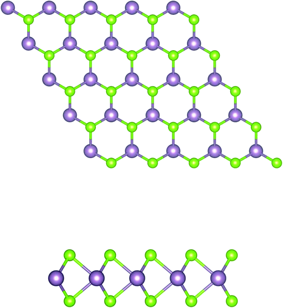 | ||
| Fig. 1 Schematic structure of a MoSe2 monolayer. The top and side views of the layered forms are shown. The purple and green balls represent the Mo and Se atoms, respectively. | ||
3.1 Formation energy and transition level of impurities in MoSe2 monolayers
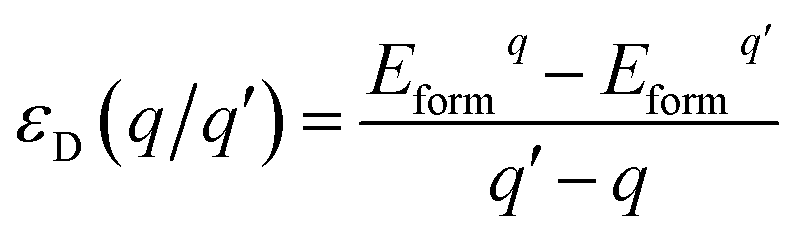
As we all know, the formation energy is the vital parameter to confirm a system’s stability. To get a more stable system, group V and VII atom doped MoSe2 monolayers were calculated in this work separately. As shown in Table 1, we list the values of dMo–X (X denotes the group V and VII atoms), MMo, MX, Mtot, Edoped and Eform (under different experimental conditions). By comparison, it is shown that the bond length dMo–X and the formation energy also increase with the increase of the radii of the group V or VII atoms. The total energy of the N-doped MoSe2 case was the lowest, which indicates that the N-doped MoSe2 monolayer is much more stable than the other considered impurity cases. To examine availability of n- and p-type doping in MoSe2, the formation energy could be calculated using the following formula:35| Eformq = E(doped)q − E(pure) − ∑niµi + q[EF + Ev + ΔV] | (1) |
 | (2) |
| 2µSe + µMo = µMoSe2 | (3) |
| System | dMo–X (Å) | MMo (µB) | MX (µB) | Mtot (µB) | Edoped (eV) | εD(q/q′) (eV) | Eform | |
|---|---|---|---|---|---|---|---|---|
| Mo-rich | Se-rich | |||||||
| N | 2.004 | 0.024 | 0.197 | 0.790 | −322.336 | 0.207 | 0.481 | 1.518 |
| P | 2.411 | 0.069 | 0.068 | 0.553 | −319.449 | 0.155 | 1.135 | 2.173 |
| As | 2.575 | 0.0 | 0.0 | 0.0 | −318.597 | 0.150 | 4.021 | 5.059 |
| F | 2.284 | 0.231 | 0.056 | 0.885 | −317.873 | 0.031 | −1.306 | −0.268 |
| Cl | 2.515 | 0.253 | 0.044 | 0.872 | −316.285 | 0.103 | 0.217 | 1.255 |
| Br | 2.650 | 0.260 | 0.055 | 0.892 | −315.621 | 0.125 | 1.025 | 2.063 |
| I | 2.821 | 0.253 | 0.062 | 0.867 | −314.975 | 0.199 | 1.563 | 2.601 |
From the above calculations, we see that the formation energy is lower under Mo-rich conditions than under Se-rich conditions, and the N-doped MoSe2 monolayer is much more stable than the other considered impurity cases. To have a better understanding, Fig. 2 is given to describe the formation energies and transition levels of group V and VII atom doped MoSe2, and we present the formation energies as a function of the Fermi level referenced to the VBM in the MoSe2 monolayers. For p-type doping cases, one can see that the formation energy curves move towards the VBM with increasing atomic number of the dopant, and this indicates that, along with the atomic number increasing, the transition level between the different charge states (0/−1) decreases. The numerical results show that the calculated transition levels are 207 meV, 155 meV, and 150 meV above the VBM for the N-, P-, and As-doped MoSe2, respectively. From the transition level data, it can be concluded that group V impurities are shallow acceptor dopants in MoSe2 monolayers. But for the case of the n-type doped system, the charge state (+1/0) transition levels are 31 meV, 103 meV, 125 meV, and 199 meV below the CBM, for the F-, Cl-, Br- and I-doped MoSe2, respectively, which indicates the halogen impurities are shallow donor dopants in MoSe2 monolayers. From these data, we can see that when the atomic number increases, the transition level of the charged system also increases. This trend is the opposite of the former, which may be attributed to the stronger electronegativity of halogen atoms compared to group V atoms. Therefore, we predicted that n-type conductivity may be engineered in the group VII atom doped MoSe2 systems via halogen atom doping. Furthermore, combining the above transition level data, the transition level of the F impurities is only 31 meV, thus we consider that F impurities can offer effective n-type carriers in MoSe2 monolayers.
 | ||
| Fig. 2 The formation energy as a function of Fermi level from the VBM to CBM for group V and VII dopant atoms. In both of the figures, the solid line represents the Mo-rich cases and the broken line represents the Se-rich cases. | ||
3.2 Electronic structures of group V and VII atoms doped in MoSe2 monolayers
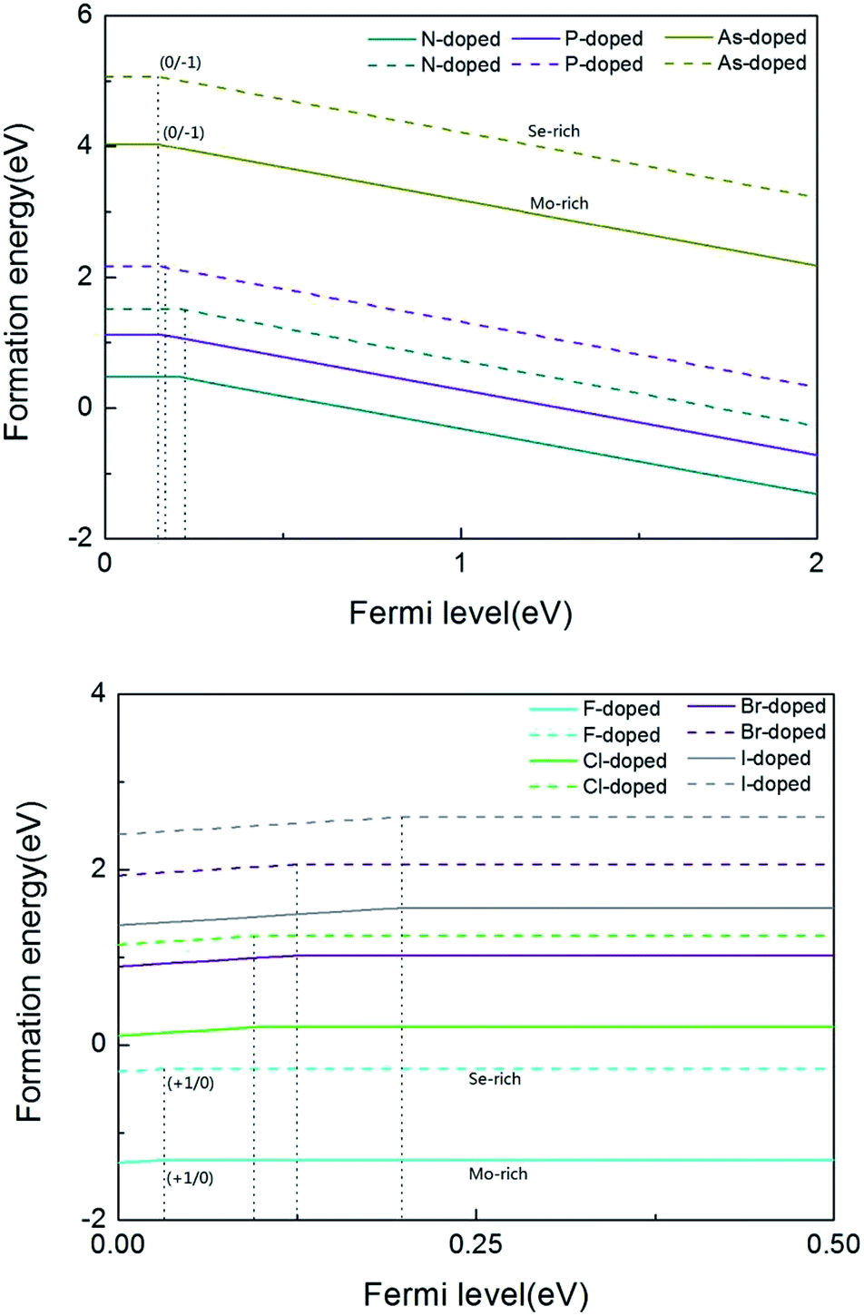
Fig. 3(a) shows the band structures for the pristine and X-doped MoSe2 monolayers using the GGA method. For the pristine MoSe2 monolayer, the direct band gap at high symmetry is about 1.51 eV, which supplies a reliable basis to confirm that the pristine monolayer is a semiconductor. Indeed, it is consistent with previous theoretical and experimental results.38 Due to the introduction of dopant atoms, an impurity state appeared in the band structures. In addition, the impurity states are close to the valance band in the N-, P-, and As-doped systems, and this signifies that the systems are p-type doped. But for the F-, Cl-, Br- and I-doped systems, the impurity states are close to the conduction band, which indicates n-type doping. From Fig. 3(a), we find that the pure MoSe2 monolayer is an intrinsic semiconductor without magnetism. However, the group V and VII atoms can induce magnetism, in addition to the As-doped system. This is due to the fact that as the atomic number increases, the bond length increases, but the bond energy decreases. The results of our calculations show that the formation energy of the As-doped system is larger than that of the N- and P-doped systems and the interaction with the host atoms is weaker. The electronegativity of As atoms is smallest compared to that of the other dopant atoms in group V and VII. More specifically, N- and F-doped systems exhibit magnetic nanomaterial properties, and the P- and As-doped systems display metallic features. Cl-, Br-, and I-doped systems exhibit half-metal features. The half-metallic (HM) gap is a valuable parameter for ensuring whether half-metallic ferromagnetic materials could be ideal electron spin injection sources for semiconductors, and is defined as the minimum of Ec and Ev, where Ec is the energy of the bottom of the minority-spin conduction band and Ev is the absolute energy value of the top of the minority-spin valence band, and both of these values are quoted with respect to the Fermi level.16,19 According to this rule, the HM gaps that we calculated for the Cl-, Br-, and I-doped systems are about 0.035 eV, 0.049 eV, and 0.071 eV, respectively. HM material with a spin polarization that is close to 100% near the Fermi level ensures the passage of the preferred spin at a high degree, and thus the Cl-, Br-, and I-doped systems may be feasible for spin filter device applications.20,39 | ||
| Fig. 3 (a) Band structures of pristine and one X-doped MoSe2 monolayer using the GGA method. The black lines and red lines represent the spin-up and spin-down components, respectively, where the Fermi level is indicated by the dotted line. (b) The band structures of typical N- and F-doped 4 × 4 × 1 MoSe2 monolayers using the GGA + U method. | ||
In addition, the previous theoretical studies on 2D Mo systems usually neglected the GGA + U method31,40 because Mo is not a strongly correlated system,41 and so a relatively small value for the on-site Coulomb interaction is sufficient for the calculated systems.42 To get more accurate results, we have recalculated it using the GGA + U method with U = 3.0 eV. The magnetic moments we calculated for the group V and VII atom doped MoSe2 systems are 0.856 µB, 0.623 µB, 0.002 µB, 1.024 µB, 0.962 µB, 0.982 µB, and 0.911 µB, respectively, which are similar to the results achieved using the GGA method in Table 1. We also choosed the N- and F-doped systems as representative cases to plot the band structure graph in Fig. 3(b), and found that it did not affect our conclusions that were drawn from using the GGA method. Thus, we hold the above view that the group V and VII atom doped systems are not sensitive to the value of U through our calculations using the GGA + U approach.
Furthermore, to more fully explain the electronic structures of MoSe2 monolayers, the total density of states (TDOS) and partial total density of states (PDOS) of the doped systems are shown in Fig. 4. As shown in the graphs, some impurity states appear in the gap, thus leading to the DOS of spin-up and spin-down systems to be asymmetric near the Fermi energy compared to that of the perfect MoSe2 monolayer. It also reveals that the local moment is mainly contributed to by the p orbital of the Se atoms and the d orbital of the Mo atoms. The hybridization between the Mo-4d and Se-4p states is associated with the weak covalency between the Mo and Se atoms. For pristine and As-doped systems, the spin-up and spin-down TDOS are symmetric, which indicates that the pure system presents a non-magnetic ground state,16 which agrees exactly with the calculated total magnetic moment 0 µB for the systems (see Table 1). But for the other doped systems, the spin-up and spin-down TDOS are asymmetric, which indicates that the systems present a magnetic ground state. These conclusions are also consistent with the results in Table 1. Moreover, the impurity states of the doped systems are mostly derived from the X-p orbitals, with a small part from the Mo-4d and Se-4p orbitals near the Fermi level. An asymmetrical distribution of the DOS can be seen between the majority spin and minority spin states, which produces magnetism in the X doped systems (except for the As-doped system), and the magnetic property mainly originates from the p–d hybridization between the p orbitals of the doped X atoms and the d orbitals of the neighboring three Mo atoms.
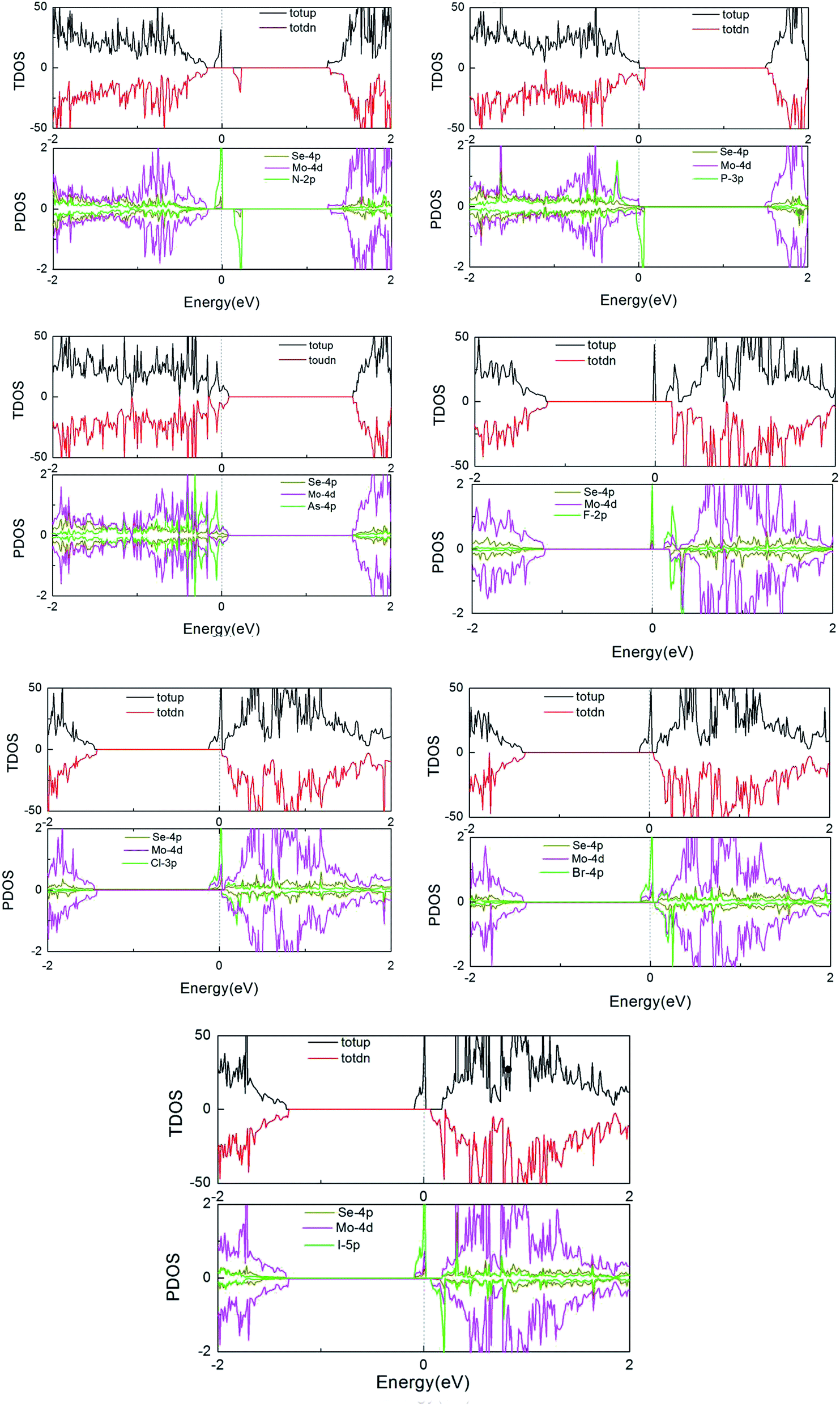 | ||
| Fig. 4 TDOS and PDOS of the X dopants and their neighboring Mo and Se atoms in the X-doped 4 × 4 × 1 MoSe2 monolayer. | ||
4. Conclusions
In summary, we investigated the electronic structure, formation energy, and transition energy level of MoSe2 based on density functional theory. The calculated results show that group V and VII atom doping can induce magnetism, except for in the As-doped system. The impurity bands of the doped systems are mostly derived from the Mo-4d orbitals near the Fermi level. N- and F-doped MoSe2 monolayers exhibit magnetic nanomaterial features. P- and As-doped MoSe2 show magnetic metallic features. The Cl-, Br-, and I-doped systems exhibit half-metallic ferromagnetism (HMF), and their half-metallic gap is about 0.035 eV, 0.049 eV, and 0.071 eV, respectively. The group V atom doped systems have p-type doping and the group VII atom doped systems can be defined as having n-type doping. The formation energy shows that the system is more stable under Mo-rich experimental conditions. In particular, for group V atom doped MoSe2, the transition level decreases with the increase of the atomic radius, but for the group VII atom doped systems, it is the opposite. By comparison, the transition energy level of F impurities is only 31 meV, thus we consider that F impurities can offer effective n-type carriers in MoSe2 monolayers. These results may be interesting for shedding light on further experimental investigations of n-type doping in MoSe2 monolayer systems.Acknowledgements
This work is supported by a Grant from the National Natural Science Foundation of China (NSFC) under the Grant No. 11504092, the Science and technology research key project of the education department of Henan province (No. 14A140012), and the High Performance Computing Center of Henan Normal University.References
- Q. H. Wang, K. Kalantar-Zadeh, A. Kis, J. N. Coleman and M. S. Strano, Nat. Nanotechnol., 2012, 7, 699–712 CrossRef CAS PubMed.
- M. Xu, T. Liang, M. Shi and H. Chen, Chem. Rev., 2013, 113, 3766–3798 CrossRef CAS PubMed.
- F. H. L. Koppens, T. Mueller, P. Avouris, A. C. Ferrari, M. S. Vitiello and M. Polini, Nat. Nanotechnol., 2014, 9, 780–793 CrossRef CAS PubMed.
- A. Kumar and P. K. Ahluwalia, Eur. Phys. J. B, 2012, 85, 186 CrossRef.
- P. R. Villeneuve and M. Piche, Phys. Rev. B: Condens. Matter Mater. Phys., 1992, 46, 4969 CrossRef.
- F. Garnier, R. Hajlaoui, A. Yassar and P. Srivastava, Science, 1994, 265, 1684–1687 CAS.
- A. Tsumura, H. Koezuka and T. Ando, Appl. Phys. Lett., 1986, 49, 1210–1212 CrossRef CAS.
- Y. Li, F. Qian, J. Xiang and C. M. Lieber, Mater. Today, 2006, 9, 18–27 CrossRef CAS.
- T. T. Wu, L. C. Wu and Z. G. Huang, J. Appl. Phys., 2005, 97, 094916 CrossRef.
- L. Schlapbach and A. Züttel, Nature, 2001, 414, 353–358 CrossRef CAS PubMed.
- A. Dillon, K. M. Jones, T. A. Bekkedahl and C. H. Kiang, Nature, 1997, 386, 377 CrossRef CAS.
- R. Mishra, W. Zhou, S. J. Pennycook, S. T. Pantelides and J. C. Idrobo, Phys. Rev. B: Condens. Matter Mater. Phys., 2013, 88, 144409 CrossRef.
- J. N. Coleman, M. Lotya, A. O’Neill, S. D. Bergin, P. J. King, U. Khan and I. V. Shvets, Science, 2011, 331, 568–571 CrossRef CAS PubMed.
- X. Zhao, C. X. Xia, T. X. Wang, X. Q. Dai and L. Yang, J. Alloys Compd., 2016, 689, 302–306 CrossRef CAS.
- X. Zhao, T. X. Wang, G. X. Wang, X. Q. Dai, C. X. Xia and L. Yang, Appl. Surf. Sci., 2016, 383, 151–158 CrossRef CAS.
- Y. Ma, Y. Dai, M. Guo, C. Niu, Y. Zhu and B. Huang, ACS Nano, 2012, 6, 1695–1701 CrossRef CAS PubMed.
- Y. C. Cheng, Z. Y. Zhu, W. B. Mi, Z. B. Guo and U. Schwingenschlögl, Phys. Rev. B: Condens. Matter Mater. Phys., 2013, 87, 100401 CrossRef.
- K. Dolui, I. Rungger, C. D. Pemmaraju and S. Sanvito, Phys. Rev. B: Condens. Matter Mater. Phys., 2013, 88, 075420 CrossRef.
- X. Zhao, P. Chen, C. X. Xia, T. X. Wang and X. Q. Dai, RSC Adv., 2016, 6, 16772–16778 RSC.
- Y. H. Zhao, G. P. Zhao, Y. Liu and B. G. Liu, Phys. Rev. B: Condens. Matter Mater. Phys., 2009, 80, 224417 CrossRef.
- Y. Li, Z. Zhou, P. Shen and Z. Chen, ACS Nano, 2009, 3, 1952–1958 CrossRef CAS PubMed.
- R. A. de Groot, F. M. Mueller, P. G. van Engen and K. H. J. Buschow, Phys. Rev. Lett., 1983, 50, 2024 CrossRef CAS.
- H. Li, X. Duan, X. Wu, X. Zhuang, H. Zhou, Q. Zhang and L. Ma, J. Am. Chem. Soc., 2014, 136, 3756–3759 CrossRef CAS PubMed.
- H. Ohno, A. Shen, F. Matsukura, A. Oiwa, A. Endo, S. Katsumoto and Y. Iye, Appl. Phys. Lett., 1996, 69, 363 CrossRef CAS.
- X. Zhao, C. X. Xia, T. X. Wang and X. Q. Dai, J. Alloys Compd., 2016, 654, 574–579 CrossRef CAS.
- J. Hafner, J. Comput. Chem., 2008, 29, 2044–2078 CrossRef CAS PubMed.
- W. Chen, E. J. Santos, W. Zhu, E. Kaxiras and Z. Zhang, Nano Lett., 2013, 13, 509–514 CrossRef CAS PubMed.
- J. P. Perdew, K. Burke and M. Ernzerhof, Phys. Rev. Lett., 1996, 77, 3865 CrossRef CAS PubMed.
- P. E. Blöchl, Phys. Rev. B: Condens. Matter Mater. Phys., 1994, 50, 17953 CrossRef.
- G. Kresse and D. Joubert, Phys. Rev. B: Condens. Matter Mater. Phys., 1999, 59, 1758 CrossRef CAS.
- Y. Ma, Y. Dai, M. Guo, C. Niu, J. Lu and B. Huang, Phys. Chem. Chem. Phys., 2011, 13, 15546–15553 RSC.
- S. L. Dudarev, G. A. Botton, S. Y. Savrasov, C. J. Humphreys and A. P. Sutton, Phys. Rev. B: Condens. Matter Mater. Phys., 1998, 57, 1505 CrossRef CAS.
- X. Du, Q. Li, H. Su and J. Yang, Phys. Rev. B: Condens. Matter Mater. Phys., 2006, 74, 233201 CrossRef.
- P. Liu, Z. Z. Qin, Y. L. Yue and X. Zuo, Chin. Phys. B, 2017, 26, 027103 CrossRef.
- C. G. Van de Walle and J. Neugebauer, J. Appl. Phys., 2004, 95, 3851–3879 CrossRef CAS.
- C. X. Xia, X. Zhao, Y. T. Peng, H. Zhang, S. Y. Wei and Y. Jia, Superlattices Microstruct., 2015, 85, 664–671 CrossRef CAS.
- S. H. Wei, Comput. Mater. Sci., 2004, 30, 337–348 CrossRef CAS.
- S. Tongay, J. Zhou, C. Ataca, K. Lo, T. S. Matthews, J. Li and J. Wu, Nano Lett., 2012, 12, 5576–5580 CrossRef CAS PubMed.
- R. A. De Groot, F. M. Mueller, P. G. Van Engen and K. H. J. Buschow, Phys. Rev. Lett., 1983, 50, 2024 CrossRef CAS.
- J. He, K. Wu, R. Sa, Q. Li and Y. Wei, Appl. Phys. Lett., 2010, 96, 082504 CrossRef.
- A. Splendiani, L. Sun, Y. Zhang, T. Li, J. Kim, C. Chim and F. Wang, Nano Lett., 2010, 10, 1271–1275 CrossRef CAS PubMed.
- S. Lebegue and O. Eriksson, Phys. Rev. B: Condens. Matter Mater. Phys., 2009, 79, 115409 CrossRef.
| This journal is © The Royal Society of Chemistry 2017 |