
 Open Access Article
 This Open Access Article is licensed under a Creative Commons Attribution-Non Commercial 3.0 Unported Licence
Thermal conductivity of multilayer dielectric films from molecular dynamics simulations
Liang Chenab,
Niru Kumaric,
Shuangtao Chena and
Yu Hou *a
*a
aSchool of Energy and Power Engineering, Xi'an Jiaotong University, Xi'an, Shaanxi 710049, China. E-mail: yuhou@mail.xjtu.edu.cn
bXi'an Jiaotong University SuZhou Academy, Su Zhou, Jiangsu 215123, China
cHP Labs, Palo Alto, CA, USA
First published on 16th May 2017
Abstract
Reducing heat dissipation across nanometer-thick dielectrics is critically important for the self-heating behavior of nanoelectronic devices such as phase change memory. In this paper, we perform molecular dynamics simulations to study the thermal conductivity of multilayer dielectric films consisting of SiO2 and Al2O3. We show that the thermal conductivity of SiO2/Al2O3 multilayer structures can be significantly reduced as compared to that of the bulk dielectrics. The thermal conductivity calculations of crystalline and amorphous multilayer structures with different period thicknesses are presented as well as the size effects. The results show the thermal transport across the crystalline SiO2/Al2O3 multilayer structures is dominated by diffuse interface scattering between thin films, while the internal phonon–phonon scattering dominates the thermal conductivity of amorphous multilayer structures. Thickness dependence are observed for the crystalline multilayer dielectric structures but not in the amorphous structures, which can be attributed to the phonon localization by the lattice termination/deformation at interfaces between crystalline films.
1. Introduction
Phase change memory (PCM), a type of high-speed non-volatile memory, relies on the different resistivity behavior of its amorphous and crystalline phases to switch between memory states.1 The amorphous/crystalline phase transition is caused by the melting and quenching processes which are induced by self-heating under an electric current pulse with a very short time period (∼the order of nanoseconds). PCM can be downscaled as small as few nanometers to make high-density PCM arrays integrated with digit circuit which have great potential for applications in storage-class memory and mass storage technologies.2,3 The main challenges for PCM to reduce the access latency and lower the requirement of programing current density as well as the energy consumption.4,5 Extensive efforts have been devoted to the development of phase change materials.6 However, the thermal design of PCM has not gain much attention. Reducing the heat loss is also a key pathway for advancing PCM technology because a good thermal confinement can facilitate the fast phase transition and reduce the programing power.7 Therefore, it is critically important to understand the thermal transport in PCM and explore novel materials/structures for good thermal insulation at nanometer scale.There are mainly two paths of heat leakage surrounding the high temperature phase change material, e.g. the electrode and the dielectrics. Several studies have been conducted to reduce the heat loss through electrodes.7 Using electrode materials with low thermal conductivity, an effective reduction of reset current has been achieved which also improves the reliability and cycling endurance.8–11 Recently, multilayer dielectric films were proposed as the surrounding dielectric of PCM cells, and the steady-state Joule-heating measurements showed a promising reduction in their thermal conductivity compared to SiO2.12 In PCM devices, reducing the thickness of dielectrics is preferred in order to make high-density arrays with high storage capacity. However, an effective thermal insulation of the PCM cell requires sufficiently thick dielectrics with high thermal resistance. The proper thermal design of the PCM requires a comprehensive understanding of the thermal transport across the dielectric structures as well as the dependence of thermal conductivity on structural parameters.
The thermal conductivity of alternating material layers, namely superlattices, has been extensively studied for semiconductor materials,13–16 e.g. Si/Ge, GaAs/AlAs, Bi2Te3/Sb2Te3, and simple Lennard-Jones solids.17,18 In those studies, the bulk materials have relatively high thermal conductivity as well as long phonon mean free path (MFP). The layer thickness is comparable to the phonon MFP, and the thermal transport in cross-plane direction can be ballistic within the layers. As a result, the phonon scattering at interfaces dominates the thermal transport while the phonon–phonon scattering within the layers becomes insignificant.19 Since the thermal boundary resistance (TBR) from a large number of interfaces plays a predominant role in the thermal transport of superlattice, the reduction its thermal conductivity can be achieved by increasing the interface density or equivalently reducing the layer thickness. In multilayer structures consisting of alternating dielectric materials (e.g. SiO2 and Al2O3), the contribution of interface scattering and internal scattering and the thermal conductivity dependence on layer thickness need further study, especially when considering the phonon MFP in low-thermal-conductivity dielectric materials is relatively small.20
In this work, we investigate the thermal transport across multilayer dielectric films consisting of SiO2 and Al2O3 in different layer thickness and total number of layers. Both crystalline and amorphous structures are considered. Non-equilibrium molecular dynamics (NEMD) simulations are performed to determine the thermal conductivity of SiO2/Al2O3 stacks with 4 nm SiO2 + 2 nm Al2O3 and 2 nm SiO2 + 1 nm Al2O3, respectively. The total thickness of the stacks ranges from 12 to 68 nm. The thermal conductivity of bulk SiO2 and Al2O3 are also presented as well as the thermal boundary conductance between SiO2 and Al2O3. The thermal conductivity from direct MD prediction is compared with the analytical estimation by combing the thermal resistance of layers and interfaces. The comparison shows different trends for the crystalline and amorphous multilayer structures. TBR contribution and thickness dependence are observed for the crystalline multilayer dielectric structures rather than the amorphous multilayer dielectric structures. The lattice dynamics calculations and localization mode analysis further reveal the phonon localization is responsible for the decrease of thermal conductivity of crystalline multilayer structures with reduced layer thickness. The present study will provide insights to understand the mechanism of thermal transport of multilayer structures of few-nanometer-thick dielectric films and to engineer the surrounding dielectrics for enhanced thermal insulation of PCM devices.
2. Models and computational methods
In this paper, BKS potential model21 with Matsui's parameterization22 is employed as the interatomic potential for all the calculations. The parameterization by Matsui shows good reliability and transferability for CaO–MgO–Al2O3–SiO2 system, and it has been verified against the lattice structures and bulk moduli. The BKS potential used in present work has the following form.where Vij is the total interatomic potential between atoms i and j. rij is the interatomic distance between atoms i and j. q is the charge peculiar of the kind of ion i. The charge of O ions in SiO2/Al2O3 system is −0.945. The charges of Si and Al ions are 1.89 and 1.4175, respectively, which can make the system neutral according to the composition ratio. A, B and C are the energy parameters. The three terms at the right hand side represent the Coulomb interaction, the Pauli repulsion energy, and the attractive van der Waals interaction, respectively.

The optimized lattice constants for crystalline SiO2 (α-quartz) and Al2O3 (corundum) are 4.91 Å and 4.76 Å in a–b plane, respectively. An initial lattice constant of 4.91 Å is used for SiO2/Al2O3 structures to prepare the multilayer structure with a periodic boundary condition in the plane direction perpendicular to the heat transfer. The a–b plane is used as the cross section to form the interface with dimensions of 2.47 nm × 2.49 nm. Slabs of crystalline lattices of each material are first generated with the conventional unit cells, e.g. SiO2 slabs of thickness of 4.1 nm and 1.9 nm, and Al2O3 slabs of thickness of 2.6 nm and 1.3 nm. The crystalline multilayer structures are formed by joining the crystalline slabs together, denoted by 4 nm-SiO2/2 nm-Al2O3 and 2 nm-SiO2/1 nm-Al2O3 as shown in Fig. 1.
 | ||
| Fig. 1 Schematic of lattice structures in NEMD simulations. | ||
In order to prepare the samples of amorphous multilayer structures, the amorphous slab of each material is first obtained starting from its crystalline lattice. A slab of crystalline lattice is generated, and a series of MD simulations are performed in order to obtain the amorphous structure. The volume of the slab is first enlarged by 20%, and melted at a high temperature of 6000 K for 100![[thin space (1/6-em)]](https://www.rsc.org/images/entities/char_2009.gif) 000 steps so that a disordered state is reached. The volume is then scaled down to its original value, and the system is equilibrated at 6000 K for another 100000 steps. In the third step, the temperature of system is quickly cooled down to 400 K, the average temperature for NEMD simulations.23 Finally, the system is equilibrated at 400 K in canonical ensemble (NVT) for 100000 steps followed by an equilibration of 100000 steps in microcanonical ensemble (NVE). The initial structure of the amorphous few-layer structure is formed by assembling the amorphous slabs of each material in the z direction. Before applying the temperature difference for the NEMD simulation, the initial amorphous few-layer structure is optimized and equilibrated first in isothermal–isobaric ensemble (NPT), then NVT and finally NVE.
000 steps so that a disordered state is reached. The volume is then scaled down to its original value, and the system is equilibrated at 6000 K for another 100000 steps. In the third step, the temperature of system is quickly cooled down to 400 K, the average temperature for NEMD simulations.23 Finally, the system is equilibrated at 400 K in canonical ensemble (NVT) for 100000 steps followed by an equilibration of 100000 steps in microcanonical ensemble (NVE). The initial structure of the amorphous few-layer structure is formed by assembling the amorphous slabs of each material in the z direction. Before applying the temperature difference for the NEMD simulation, the initial amorphous few-layer structure is optimized and equilibrated first in isothermal–isobaric ensemble (NPT), then NVT and finally NVE.
A. Non-equilibrium molecular dynamics simulations
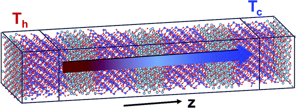
MD simulations are performed using the Large-Scale Atomic/Molecular Massively Parallel Simulator (LAMMPS).24,25 The schematic of the SiO2/Al2O3 multilayer structures is shown in Fig. 1. In the NEMD simulations, periodic boundary conditions are applied in the x and y directions while the two ends in the z direction are set free. A time step of 1 fs is used in all MD simulations. In order to reduce the stress, the initial structure is optimized and equilibrated in the NPT. Then NVT and NVE simulations are carried out to obtain the initial structure at specified temperature. The NEMD simulations are performed under NVE with specified temperature difference.As shown in Fig. 1, a heating bath and a cooling bath are applied at left end and right end of the system, respectively. The heating/cooling bath is 3 nm long with ∼2000 atoms. The constant temperatures at 410 K and 390 K are maintained by rescaling the velocities of atoms in the heating and cooling baths, respectively.26 In order to reach the steady state, we first perform NEMD simulations for 10 ns before sampling. Then we sample the temperature along the z direction for another 20 ns. According to Fourier's law, the thermal conductivity is calculated as k = ![[q with combining dot above]](https://www.rsc.org/images/entities/i_char_0071_0307.gif) /(AdT/dx), where , A and dT/dx are the heat transfer rate, the cross-section area and the temperature gradient in heat flux direction, respectively. The linear fitting of the cumulative energy change and the temperature profiles are performed to determine the heat transfer rate and temperature gradient, respectively.
/(AdT/dx), where , A and dT/dx are the heat transfer rate, the cross-section area and the temperature gradient in heat flux direction, respectively. The linear fitting of the cumulative energy change and the temperature profiles are performed to determine the heat transfer rate and temperature gradient, respectively.
B. Phonon dispersion and participation ratio
In dielectric materials, phonons are the energy carriers responsible for the heat conduction. In order to gain more insights of the mechanism of the thermal transport in multilayer dielectrics, we calculate the phonon dispersions, group velocities, and participation ratio. Based on the BKS potential and lattice structures above mentioned, the vibrational eigen-modes are obtained from the lattice dynamics using the general utility lattice program (GULP).27 The phonon group velocities are calculated from the phonon dispersion relations using central difference scheme, v(s,q) = ∂ωs/∂q, where s and q are the indices of phonon polarization and wave vector, respectively.The phonon participation ratio is used to quantitatively characterize the localization of each mode, which can be calculated from the following formulism.28
![[e with combining right harpoon above (vector)]](https://www.rsc.org/images/entities/i_char_0065_20d1.gif) s,q is the eigenvector of mode (s,q), and i runs over all the N atoms in the system. According to this definition, the participation ratio is on the order of 1 for the spatially extended modes while it can be as small as 1/N for the completely localized mode.
s,q is the eigenvector of mode (s,q), and i runs over all the N atoms in the system. According to this definition, the participation ratio is on the order of 1 for the spatially extended modes while it can be as small as 1/N for the completely localized mode.
3. Results and discussion
A. Thermal resistance analysis of multilayer structures
The thermal conductivities of both the crystalline and amorphous SiO2 and Al2O3 are calculated using NEMD simulations.23 The thickness dependence of thermal conductivity of crystalline SiO2 and Al2O3 is shown in Fig. 2. It can be observed that both the thermal conductivities of crystalline SiO2 and Al2O3 increases as the thickness increases which indicates the mean free path longer than the simulation domain is limited. A linear relation between 1/k and 1/L can be observed as shown in Fig. 2(b), and it is consistent with the Matthiessen's rule as described by Schelling et al.29 The relation is linearly extrapolated to L → ∞, yielding thermal conductivities of 7.0 W (m−1 K−1) and 7.9 W (m−1 K−1) for bulk crystalline SiO2 and Al2O3, respectively. Based on NEMD simulations, the thermal conductivities of amorphous SiO2 and Al2O3 are 1.7 W (m−1 K−1) and 2.2 W (m−1 K−1), respectively. The predictions are comparable with the experimental results in literatures, e.g. 1.0–1.5 W (m−1 K−1) for SiO2 (ref. 30–32) and 1.8–2.8 W (m−1 K−1),33 and the deviations may be due to the difference in density and the error from the empirical potential model. The thickness dependence is not observed for the amorphous SiO2 or Al2O3 due to the small phonon mean free path in the amorphous structures.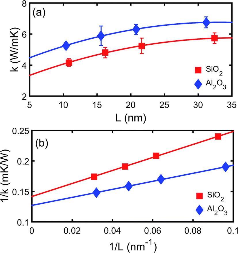 | ||
| Fig. 2 Thermal conductivity of (a) crystalline SiO2 and (b) crystalline Al2O3 films as a function of thickness. | ||
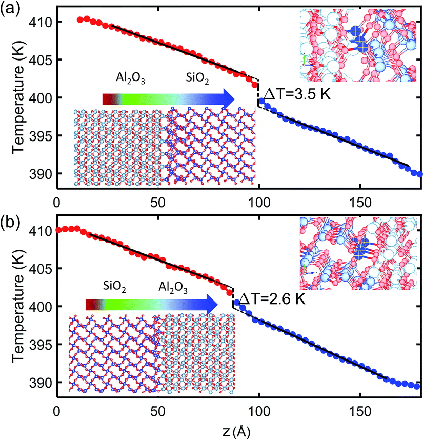
The TBR between crystalline SiO2 and Al2O3 is calculated from NEMD simulations at two interfaces of different bonding as illustrated by the insets of Fig. 3. The Al2O3/SiO2 interface shown in Fig. 3(a) has Al and Si atoms aligned at the same x–z plane, and fewer O atoms are available to form Si–O and Al–O bonds at the interface. The SiO2/Al2O3 interface shown in Fig. 3(b) has Al and Si atoms staggered, and more O atoms can be found at the interface to form a good contact with increased Si–O and Al–O bonds. A zoom-in of the bonding at interface are shown in Fig. 3 which can clearly shows the difference of Si–O at interfaces of the two structures. In both structures, there are totally 30 Al atoms at interface all of which form bonds with O atoms in SiO2. In the Al2O3/SiO2 interface with poor contact, around 16 Si atoms can form bonds with O in Al2O3. In SiO2/Al2O3 interface with good contact, all the 30 Si atoms can form bonds with Al2O3. As a result, the bond densities across the interfaces are 7.8 per nm2 and 10.2 per nm2. According to the temperature profiles along the direction of heat conduction shown in Fig. 3, the linear temperature profiles in SiO2 and Al2O3 are extrapolated to the interface. Interfacial temperature differences of 3.5 K and 2.6 K are obtained for the two interfaces. The corresponding TBRs (R1 and R2) at 400 K are 0.67 m2 K GW−1 and 0.41 m2 K GW−1, respectively. It can also been observed that the temperature gradient within SiO2 and Al2O3 becomes larger near the interface, contributing to the interfacial temperature difference. This is because the phonon scattering is increased by the tangling of lattices near the interface.
 | ||
| Fig. 3 Temperature profiles at interfaces between crystalline SiO2 and Al2O3 of different bonding: (a) Al2O3/SiO2 interface with poor contact; (b) SiO2/Al2O3 interface with good contact. The solid lines indicate the linear fitting while the dashed lines are the extrapolations. The upper right insets show the zoom-in of the Si bonded with O in Al2O3 at the interfaces. | ||
If the phonon transport through each film is fully ballistic, the film resistances become negligible and the TBRs dominate the thermal conductivity of multilayer structures. The effective thermal conductivity keff can be determined according to the thermal resistance analysis, (tSiO2 + tAl2O3)/keff = R1 + R2, where t and R denotes the thickness and the thermal boundary resistance, respectively. The effective thermal conductivities are 6.2 W (m−1 K−1) and 3.0 W (m−1 K−1) for 4 nm-SiO2/2 nm-Al2O3 and 2 nm-SiO2/1 nm-Al2O3 multilayer structures, respectively. Including the thermal resistance of alternating films, the effective thermal conductivity of SiO2/Al2O3 multilayer structures can be estimated from the resistance analysis, e.g. (tSiO2 + tAl2O3)/keff = (t/k)SiO2 + (t/k)Al2O3 + R1 + R2. The effective thermal conductivities are 3.4 W (m−1 K−1) and 2.1 W (m−1 K−1) for 4 nm-SiO2/2 nm-Al2O3 and 2 nm-SiO2/1 nm-Al2O3 multilayer structures, respectively. Since the bulk thermal conductivity is used for films of different thickness, the film-thickness dependence of the effective thermal conductivities of multilayer structures is caused by the interface density. The comparison of different resistance terms indicates the TBR contributes about 54% and 71% for the two multilayer structures. Considering the decrease of thermal conductivity of thin films, the film thermal resistance will increase, leading to further reduction of the effective thermal conductivity of the crystalline multilayer structures. However, the NEMD simulations on the amorphous structures show negligible temperature difference at interface between amorphous SiO2 and Al2O3, which indicates negligible TBR. The amorphous structure enhance the contact, and more bonding can be formed via the O atoms between SiO2 and Al2O3. The other reason for the negligible TBR is that the phonon mean free path inside the films are very small and are not affected by the interface.
B. Direct NEMD simulations of multilayer structures
Fig. 4 shows the temperature profile across the crystalline SiO2/Al2O3 multilayer structures with total thickness of 26.5 nm. The lower insets under the temperature profiles indicate the alternating SiO2 and Al2O3 layers and the location of their interfaces. In both 2 nm-SiO2/1 nm-Al2O3 and 4 nm-SiO2/2 nm-Al2O3 multilayer structures, it can be observed that a noticeable temperature drop repeatedly occurs at the SiO2/Al2O3 interfaces that are marked in the lower inset. As shown in Fig. 4(a), the last temperature drop near the cooling bath end is indicated by the circle with an arrow pointing to the zoom-in of the interface atomic structures. According to the discussion in Section 3A, this interface structure has fewer bond connections, leading to a relatively large TBR as well as temperature drop, which is similar with the one as shown in Fig. 3.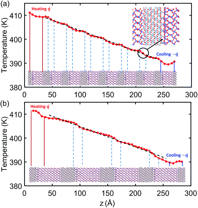 | ||
| Fig. 4 Temperature profiles across (a) 2 nm-SiO2/1 nm-Al2O3 crystalline multilayer structures and (b) 4 nm-SiO2/2 nm-Al2O3 crystalline multilayer structures. The dashed line is the linear fitting. | ||
The temperature profiles in Fig. 4(a) also indicate that temperature variations are quite small within the 2 nm SiO2 films and 1 nm Al2O3 films. So the thermal transport in the 2 nm-SiO2/1 nm-Al2O3 multilayer structures is dominated by the interface phonon scattering while the phonon transport across the films is nearly ballistic. As the film thickness is increased, as in Fig. 4(b), the temperature variations (∼2.5 K) within the films has exceeded the temperature differences (∼3.5 K) at the interfaces. As a result, both the interfacial phonon scattering and the internal phonon–phonon scattering are important in determining the thermal conductivity of crystalline SiO2/Al2O3 multilayer structures with thicker layers. For all the amorphous SiO2/Al2O3 multilayer structures in the present work, the temperature drop at SiO2 and Al2O3 interface is not observed, and the temperature profile is linear and smoother except for the region near the heat baths. This observation is in agreement with the above results of the NEMD simulations SiO2/Al2O3 interface. Therefore, the thermal conductivity of amorphous SiO2/Al2O3 multilayer structures should only depend on the internal phonon–phonon scattering.
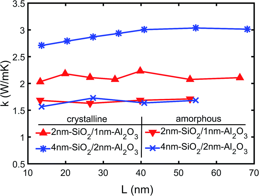
The thermal conductivity of the multilayer structures is calculated using the temperature gradient from the linear fitting of the temperature profiles as shown in Fig. 4. The NEMD simulations are performed on both 2 nm-SiO2/1 nm-Al2O3 and 4 nm-SiO2/2 nm-Al2O3 multilayer structures with total thicknesses ranging from 13.6 nm to 68.2 nm. The predictions of the effective thermal conductivity are shown in Fig. 5. The thermal conductivity of 4 nm-SiO2/2 nm-Al2O3 multilayer structures shows size dependence when the total thickness is below 40 nm. The size dependence indicates the contribution of phonon–phonon scattering is non-negligible. In multilayer structures consisting of thick slabs, phonons can have relatively large mean free path and transmit across interfaces. Those phonons are finally scattered at boundaries due to the small domain size, and the increase of the domain size can allow the presence of phonons with longer mean free path as well as increasing the thermal conductivity. However, in multilayer structures consisting of thin slabs, the interface scattering is so intense that the thermal conductivity is determined mainly by the TBR at interfaces and does not show any dependence on the domain size.
 | ||
| Fig. 5 Thermal conductivity of SiO2/Al2O3 multilayer structures as a function of thickness. | ||
As shown in Fig. 5, the thick 4 nm-SiO2/2 nm-Al2O3 multilayer structure has thermal conductivity approaching 3.0 W (m−1 K−1) which is about 50% higher than that (∼2.1 W (m−1 K−1)) of the 2 nm-SiO2/1 nm-Al2O3 multilayer structure. Both the predictions of the two multilayer structures by the direct NEMD simulations agree with the results of above thermal resistance analysis (Section 3A) which incorporates both the film resistances and TBRs. For the 4 nm-SiO2/2 nm-Al2O3 multilayer structure, the direct NEMD prediction is slightly lower than the prediction (3.4 W (m−1 K−1)) of the above thermal resistance analysis (Section 3A). This can be because the use of the bulk thermal conductivity which is expected to be higher than that of the thin films. However, the TBR resistances can account for 71% of the total resistance for the 2 nm-SiO2/1 nm-Al2O3 multilayer structure. So the variations of thermal resistance of thin films have little effect on its effective thermal conductivity, and the predictions by the direct NEMD simulations match well with the results (2.1 W (m−1 K−1)) of thermal resistance analysis for 2 nm-SiO2/1 nm-Al2O3 multilayer structures.
Fig. 5 also shows the variations of the effective thermal conductivity of amorphous SiO2/Al2O3 multilayer structures with difference film thickness and total thickness. It can be observed that neither the film thickness nor the total thickness has any effect on the thermal conductivity of amorphous SiO2/Al2O3 multilayer structures. The mean value of the predictions shown in Fig. 5 is 1.7 W (m−1 K−1) which is same with the thermal conductivity of amorphous SiO2 but smaller than the amorphous Al2O3. Since the TBR between amorphous SiO2 and Al2O3 is negligible, the thermal conductivity of the amorphous Al2O3 films is lowered in amorphous SiO2/Al2O3 multilayer structures. It should be noted that this observation is only valid for the nanometer thick films. As the film thickness increases to tens of nanometer, the effects of SiO2 on the thermal conductivity of amorphous Al2O3 film will diminish.
C. Vibrational mode analysis
The phonon eigen vectors and frequencies are obtained from lattice dynamics calculations using GULP. The unit cells are used for bulk crystalline SiO2 and Al2O3, while one SiO2/Al2O3 slab with cross-sectional area of 2.5 nm × 2.5 nm and different layer thicknesses is used as the cell of both the crystalline and the amorphous multilayer structures. Fig. 6 shows the acoustic branches of phonon dispersion curves and group velocities of bulk SiO2, bulk Al2O3, 4 nm-SiO2/2 nm-Al2O3 slab, and 2 nm-SiO2/1 nm-Al2O3 slab. The maximum group velocities of phonons (longitudinal) in bulk SiO2 and bulk Al2O3, are around 9 km s−1 and 11 km s−1, respectively. Compared with the bulk materials, the group velocities of the longitudinal phonons in 4 nm-SiO2/2 nm-Al2O3 slab and 2 nm-SiO2/1 nm-Al2O3 slab are reduced to 7.5 km s−1 and 6.5 km s−1, respectively. The group velocities of the transverse acoustics phonons remain similar with those in the bulk materials. In the multilayer structures, the presence of SiO2/Al2O3 interfaces increases the boundary scattering of the longitudinal phonons which propagate in the direction perpendicular to the interface rather than the transverse phonons. Acoustic phonons with high group velocity and long mean free path are responsible for the thermal transport. The increased scattering of longitudinal phonon modes leads to the reduction of the thermal conductivity of multilayer structures.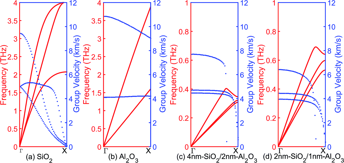 | ||
| Fig. 6 Acoustic branches of phonon dispersion curves and group velocities of (a) SiO2, (b) Al2O3, (c) 4 nm-SiO2/2 nm-Al2O3 multilayer structures, and (d) 2 nm-SiO2/1 nm-Al2O3 multilayer structures. | ||
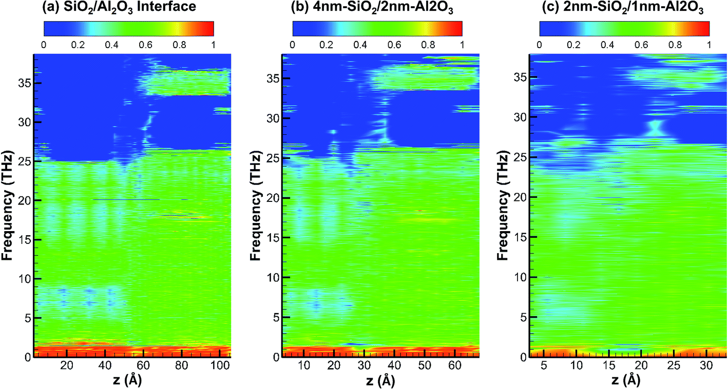
The lattice tangling and deformation near the interfaces can also increase the phonon scattering. Mode localization of phonons is believed to be responsible for the reduction of thermal conductivity in materials with lattice defects or disorder systems.34 The phonon participation ratio quantitatively characterizes the mode localization of phonons. In order to represent the spatial variations of mode location near the SiO2/Al2O3 interfaces, the structures are split into bins with a width of 3 Å, and the phonon participation ratio is calculated for atoms in each bin.
Fig. 7 shows the partition ratio of phonons as a function of location for crystalline SiO2/Al2O3 interface, crystalline 4 nm-SiO2/2 nm-Al2O3 slab, and crystalline 2 nm-SiO2/1 nm-Al2O3 slab. For all the three systems, the phonons are partially localized with PR around 0.5 in the frequency range from 2 THz to 25 THz. Above 25 THz, the PR only show some partially localized modes in SiO2 from 32 THz to 40 THz. It can be observed that the acoustic phonons with frequency below 2 THz mainly consists of delocalized modes with PR around 1 in the first two systems of SiO2/Al2O3 interface and 4 nm-SiO2/2 nm-Al2O3 slab. However, in the 2 nm-SiO2/1 nm-Al2O3 slab, the portion of modes with high PR diminishes indicating those phonon modes become partially localized. Around the SiO2/Al2O3 interface in the 2 nm-SiO2/1 nm-Al2O3 slab, the PR is nearly zero which indicates the mode localization near the interfaces. With the decrease of film thickness, the lattice deformation can extend to the entire film, intensify the phonon scattering and mode localization, and lead to the decrease of thermal conductivity of multilayer structures.
 | ||
| Fig. 7 Partition ratio of phonons as a function of location for crystalline SiO2/Al2O3 interface, 4 nm-SiO2/2 nm-Al2O3 crystalline structures, and 2 nm-SiO2/1 nm-Al2O3 crystalline structures. | ||
Fig. 8 shows the partition ratio of phonons as a function of location for amorphous 4 nm-SiO2/2 nm-Al2O3 slab, and amorphous 2 nm-SiO2/1 nm-Al2O3 slab. It can be observed that there is little difference of PR distribution between the two amorphous structures. As compared with the PR distribution of crystalline structures as shown in Fig. 7, the PR becomes smaller for the amorphous structures, especially for the region above 20 THz for both SiO2 and Al2O3. The observations from Fig. 8 indicate presence of SiO2 film leads to the localization of phonons in Al2O3 as well as the reduction of its thermal conductivity. Therefore, the amorphous SiO2 and Al2O3 structures exhibit thermal conductivity same with amorphous SiO2 regardless of the slightly higher thermal conductivity of amorphous Al2O3.
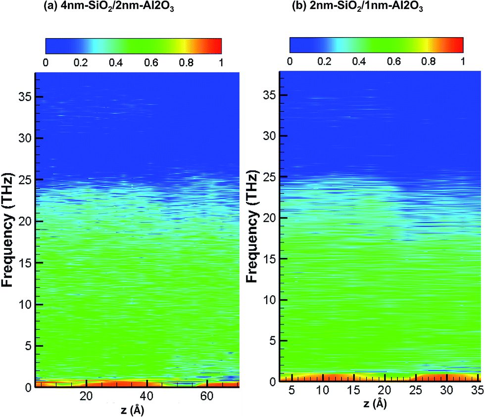 | ||
| Fig. 8 Partition ratio of phonons as a function of location for 4 nm-SiO2/2 nm-Al2O3 amorphous structures and 2 nm-SiO2/1 nm-Al2O3 amorphous structures. | ||
4. Conclusions
In summary, we have studied the thermal transport in both the crystalline and amorphous SiO2/Al2O3 multilayer structures using NEMD simulations and lattice dynamics calculations. The NEMD predictions of thermal conductivity are compared with the results of thermal resistance analysis. The results suggest both the TBR and film resistance are important for calculating the thermal conductivity of crystalline multilayer dielectric structures. The film resistance arising from internal phonon–phonon scattering becomes equally important as TBR in crystalline SiO2 films of thickness around 4 nm. The thermal conductivity of amorphous SiO2 and Al2O3 structures shows no dependence on the film thickness or total thickness. Based on the lattice dynamics calculations and localization mode analysis, we find the phonon localization is responsible for the decrease of thermal conductivity of crystalline multilayer structures, especially in structures consisting of very thin films. Our study is expected to be valuable for the thermal insulation design of PCM devices and to provide insights for understanding the mechanism of thermal transport of multilayer structures of few-nanometer-thick dielectric films.Acknowledgements
This work was supported by the China Postdoctoral Science Foundation (2015M580844), the Fundamental Research Funds for the Central Universities (2012JDGZ03), and the Natural Science Foundation of Jiangsu Province (BK20160388).References
- F. Dirisaglik, G. Bakan, Z. Jurado, S. Muneer, M. Akbulut, J. Rarey, L. Sullivan, M. Wennberg, A. King and L. Zhang, Nanoscale, 2015, 7, 16625–16630 RSC.
- K. H. Kim, S. Gaba, D. Wheeler, J. M. Cruz-Albrecht, T. Hussain, N. Srinivasa and W. Lu, Nano Lett., 2012, 12, 389–395 CrossRef CAS PubMed.
- R. E. Simpson, M. Krbal, P. Fons, A. V. Kolobov, J. Tominaga, T. Uruga and H. Tanida, Nano Lett., 2010, 10, 414–419 CrossRef CAS PubMed.
- Y. Cassuto, S. Kvatinsky and E. Yaakobi, 2013 IEEE International Symposium on Information Theory Proceedings, 2013, pp. 156–160 Search PubMed.
- M. Upadhyay, S. Abhaya, S. Murugavel and G. Amarendra, RSC Adv., 2014, 4, 3691 CAS.
- D. Ielmini and A. L. Lacaita, Mater. Today, 2011, 14, 600–607 CrossRef CAS.
- Z. J. Li, R. G. D. Jeyasingh, J. Lee, M. Asheghi, H. S. P. Wong and K. E. Goodson, IEEE Trans. Electron Devices, 2012, 59, 3561–3567 CrossRef CAS.
- A. Sood, S. B. Eryilmaz, R. Jeyasingh, J. Cho, M. Asheghi, H. S. P. Wong and K. E. Goodson, Presented in part at the IEEE Intersociety Conference on Thermal and Thermomechanical Phenomena in Electronic Systems (ITHERM) 2014, Orlando, FL, USA, May 27–30, 2014 Search PubMed.
- J. Y. Wu, M. Breitwisch, S. Kim, T. H. Hsu, R. Cheek, P. Y. Du, J. Li, E. K. Lai, Y. Zhu, T. Y. Wang, H. Y. Cheng, A. Schrott, E. A. Joseph, R. Dasaka, S. Raoux, M. H. Lee, H. L. Lung, C. Lam and I. M. P. J. Project, 2011 IEEE International Electron Devices Meeting, 2011, 3.2.1–3.2.4 Search PubMed.
- C. Kim, D.-S. Suh, K. H. P. Kim, Y.-S. Kang, T.-Y. Lee, Y. Khang and D. G. Cahill, Appl. Phys. Lett., 2008, 92, 013109 CrossRef.
- E. Bozorg-Grayeli, J. P. Reifenberg, M. A. Panzer, J. A. Rowlette and K. E. Goodson, IEEE Trans. Electron Devices, 2011, 32, 1281–1283 CrossRef CAS.
- S. W. Fong, A. Sood, L. Chen, N. Kumari, M. Asheghi, K. E. Goodson, G. A. Gibson and H. S. P. Wong, J. Appl. Phys., 2016, 120, 2201–2665 CrossRef.
- M. N. Luckyanova and G. Chen, Science, 2012, 338, 936–939 CrossRef CAS PubMed.
- S. Kwon, M. C. Wingert, J. Zheng, J. Xiang and R. Chen, Nanoscale, 2016, 8, 13155–13167 RSC.
- J. C. Caylor, K. Coonley, J. Stuart, T. Colpitts and R. Venkatasubramanian, Appl. Phys. Lett., 2005, 87, 023105 CrossRef.
- J. H. Kim, Y. C. Jung, S. H. Suh and J. S. Kim, J. Nanosci. Nanotechnol., 2006, 6, 3325–3328 CrossRef CAS PubMed.
- E. S. Landry, M. I. Hussein and A. J. H. Mcgaughey, Phys. Rev. B: Condens. Matter Mater. Phys., 2008, 77, 998–1002 CrossRef.
- J. E. Turney, E. S. L. Ry, A. J. H. Mcgaughey and C. H. Amon, Phys. Rev. B: Condens. Matter Mater. Phys., 2009, 70, 7715–7722 Search PubMed.
- Y. Chalopin, K. Esfarjani, A. Henry, S. Volz and G. Chen, Phys. Rev. B: Condens. Matter Mater. Phys., 2012, 85, 1077–1082 CrossRef.
- A. J. H. Mcgaughey and M. Kaviany, Int. J. Heat Mass Transfer, 2004, 47, 1799–1816 CrossRef CAS.
- B. W. van Beest, G. J. Kramer and R. A. van Santen, Phys. Rev. Lett., 1990, 64, 1955–1958 CrossRef CAS PubMed.
- M. Matsui, Mineral. Mag., 1994, 58, 571–572 Search PubMed.
- L. Chen, Z. Huang and S. Kumar, RSC Adv., 2014, 4, 35852–35861 RSC.
- W. M. Brown, P. Wang, S. J. Plimpton and A. N. Tharrington, Comput. Phys. Commun., 2011, 182, 898–911 CrossRef CAS.
- S. Plimpton, J. Comput. Phys., 1995, 117, 1–19 CrossRef CAS.
- L. Chen, X. Wang and S. Kumar, Sci. Rep., 2015, 5, 12763 CrossRef CAS PubMed.
- J. D. Gale, J. Chem. Soc., Faraday Trans., 1997, 93, 629–637 RSC.
- H. R. Seyf and A. Henry, J. Appl. Phys., 2016, 120, 061605 CrossRef.
- P. K. Schelling, S. R. Phillpot and P. Keblinski, Phys. Rev. B: Condens. Matter Mater. Phys., 2002, 65, 144306 CrossRef.
- H. C. Chien, D. J. Yao, M. J. Huang and T. Y. Chang, Rev. Sci. Instrum., 2008, 79, 054902 CrossRef PubMed.
- T. Yamane, N. Nagai, S. Katayama and M. Todoki, J. Appl. Phys., 2002, 91, 9772–9776 CrossRef CAS.
- A. J. Griffin Jr, F. R. Brotzen and P. J. Loos, J. Appl. Phys., 1994, 75, 3761–3764 CrossRef.
- R. M. Costescu, D. G. Cahill, F. H. Fabreguette, Z. A. Sechrist and S. M. George, Science, 2004, 303, 989–990 CrossRef CAS PubMed.
- Y. Zhou, Z. X. Guo, H. Y. Cao, S. Y. Chen, H. J. Xiang and X. G. Gong, Nanoscale, 2016, 8, 17815 RSC.
| This journal is © The Royal Society of Chemistry 2017 |