DOI:
10.1039/C7RA04414C
(Paper)
RSC Adv., 2017,
7, 26202-26210
Solution processed double-decked V2Ox/PEDOT:PSS film serves as the hole transport layer of an inverted planar perovskite solar cell with high performance†
Received
19th April 2017
, Accepted 10th May 2017
First published on 17th May 2017
Abstract
In this paper, we have reported a high-performance inverted planar perovskite solar cell (PSC) with double-decked hole transport layer (HTL) sandwiched between the indium tin oxide (ITO) electrode and the perovskite photoactive layer. The double-decked HTL film is fabricated by coating inorganic vanadium oxide (V2Ox) layer and poly(3,4-ethylene dioxy-thiophene)–poly(styrene sulfonate) (PEDOT:PSS) layer. In this study, double-decked V2Ox/PEDOT:PSS HTL film can improve the optoelectronic properties of PSC device. It has been found that the double-decked V2Ox/PEDOT:PSS film plays a crucial role in enhancing charge transfer rate and suppressing electron–hole pair recombination. The valence of vanadium in the V2Ox has been changed by adjusting the molar ratio of V2O5 to H2O2. The PSC can reach its best performance when V2O5 and H2O2 react at a molar ratio of 1![[thin space (1/6-em)]](https://www.rsc.org/images/entities/char_2009.gif) :60. In addition, the concentration of the V2Ox aqueous solution has also been changed to optimize performance of PSC. Hence, the device with double-decked V2Ox/PEDOT:PSS HTL film can increase the power conversion efficiency (PCE) to 15.86%, higher than that of reference device with PEDOT:PSS (13.56%). Besides, compared with reference device, our device has a better repeatability in the preparation process.
:60. In addition, the concentration of the V2Ox aqueous solution has also been changed to optimize performance of PSC. Hence, the device with double-decked V2Ox/PEDOT:PSS HTL film can increase the power conversion efficiency (PCE) to 15.86%, higher than that of reference device with PEDOT:PSS (13.56%). Besides, compared with reference device, our device has a better repeatability in the preparation process.
1. Introduction
Due to its excellent photo-electronic properties including low exciton binding energy (∼30 meV),1 high extinction coefficient (∼104–105 cm−1),2,3 and long carrier diffusion lengths in thin films (>1 μm),4,5 the organic inorganic halide perovskite-based solar cell (PSC) have attracted considerable attention in the field of solar cells and made remarkable progress in recent years.6–9 Since 2009, the power conversion efficiency (PCE) of PSC has been increased from 3.8% to 22.1%,10,11 which is unexpected and unprecedented in the field of organic photovoltaics. The PSC can be divided into two types: one with scaffold metal oxide layer and the other without the scafford metal oxide layer like perovskite active layer sandwiched between the hole transport layer (HTL) and electron transport layer (ETL).12–15 The scaffold metal oxide layers have to be prepared under high-temperature conditions, such as Al2O3 or TiO2 on indium tin oxide (ITO) or fluorine doped tin oxide (FTO).16 The planar heterojunction (PHJ) PSC without the scafford metal oxide layer can also be classified into two categories: regular configuration (n–i–p, ETL/CH3NH3PbI3−xClx/HTL),17 and inverted configuration (p–i–n, HTL/CH3NH3PbI3−xClx/ETL).18 Owing to its low-temperature fabrication method, excellent performance and sharply-reduced hysteresis,19 PSC with inverted p–i–n structure will have a promising prospect in the future.
The poly(3,4-ethylene dioxy-thiophene)–poly(styrene sulfonate) (PEDOT:PSS) is usually used as HTL to enhance crystallinity of the perovskite layer film.20–22 We find it easy to collect the holes via the PEDOT:PSS layer, because PEDOT:PSS has many advantages over others such as good conductivity, smooth morphology, high work function (WF) and high transparency.23 The PCE of the inverted planar PSCs has been improved significantly by PEDOT:PSS HTL film. What merits much attention is that lots of research works have been carried out to enhance performances of PSCs, except PEDOT:PSS HTL film.24,25 Some researches have been conducted to use inorganic transition metal oxides including nickel oxide (NiOx),26–29 lead sulfide (PbS),30 and molybdenum oxide (MoOx)31–33 as the HTL film. The conduction levels of the oxides are much higher than the lowest occupied molecular orbital (LOMO) of the organic layers, which can prevent electrons from transporting in the wrong directions and improve the photo current of PSCs. However, most transition metal oxides films are thermally evaporated onto the substrates in vacuum and will hardly be applied to commercial production process of PSC devices due to its high cost.34,35 Recently, some techniques based on a lower-cost, simpler and more controllable approach have been reported.36 Some solution-processed bilayer HTLs have been used in solar cells, such as graphene oxide (GO)/PEDOT:PSS,37 MoO3/PEDOT:PSS,38 and PEDOT:PSS/vanadium oxide (V2Ox).39 Whereas, these cells do not show a higher PCE. Here we use double-decked V2Ox/PEDOT:PSS as HTL of PSCs, by contrast, the higher efficiency and better repeatability of the devices has been achieved by changing the valence of vanadium of double-decked V2Ox/PEDOT:PSS film.
The vanadium pentoxide (V2O5) and its derivative compounds have been researched intensively due to their redox activity.40–42 The V2Ox can be obtained by a simple method of synthesis that uses V2O5 and hydrogen peroxide (H2O2) as starting material at a low temperature. Through this method, the vanadium element produces a variety of binary compounds with the chemical general formula VO2+x (−0.5 ≤ x ≤ 0.5), such as V2O3, VO2, V2O5, V3O7, V4O9, V6O13.43 The V2Ox with different valences can be prepared by controlling the molar ratio of V2O5 to H2O2. In this work, the double-decked V2Ox/PEDOT:PSS films prepared by spin-coating V2Ox and PEDOT:PSS solution can serve as the HTL to enhance charge transfer rate and suppress electron–hole pair recombination in PSCs. Here we report a high-performance inverted planar PSC device with the structure of ITO/V2Ox/PEDOT:PSS/CH3NH3PbI3−xClx/the phenyl-C61-butyric acid methyl ester (PCBM)/Ag. The maximum PCE of 15.86% has been achieved by controlling the optimum concentration of the V2Ox solution. An average power conversion efficiency (PCEAVE) of has been increased significantly from 11.85% (the PCEAVE of 30 reference devices with PEDOT:PSS HTL) to 14.97% (the PCEAVE of 120 controllable devices with the double-decked V2Ox/PEDOT:PSS HTL).
2. Experimental
2.1 Materials and preparation
Chlorobenzene (C6H5Cl), hydrogen iodide (HI), methylamine (CH3NH2), hydrogen peroxide (H2O2, 30%) and V2O5 powder were purchased from Shanghai Chemical Industry Co. The PEDOT:PSS was bought from Heraeus (Germany). PbCl2 (99.999%) and N,N-dimethylformamide (DMF) (anhydrous, amine free; 99.9%) were purchased from Alfa-Aesar. The PC61BM was produced by Nichem Fine Technology Co., Ltd. (Taiwan). CH3NH3I was synthesized by CH3NH2 and HI according to the reported procedure.44 CH3NH3PbI3−xClx solutions were fabricated by solubilizing CH3NH3I and PbCl2 in DMF with a molar ratio of 3:1, and agitating the compound in a glove box filled with N2 at 60 °C for 12 h. PCBM solutions were manufactured by dissolving PCBM powder in chlorobenzene and churning the mixture in a N2 glove box for 12 h, with an optimized concentration of 20 mg mL−1.
2.2 Fabrication of the double-decked V2Ox/PEDOT:PSS film
First, V2O5 aqueous solution was manufactured by dissolving 15 mg of V2O5 powder in 5 mL of deionized water and churning the mixture in air at room temperature for 30 min, with a concentration of 3 mg mL−1. Second, the 0.6 mL of H2O2 aqueous solutions (30%) was added to V2O5 aqueous solution, the mixture was stirred for 10 min and let set for 10 h or more. As a result, the V2Ox aqueous solution was prepared. V2Ox aqueous solution prepared was filtered through a 0.22 μm pore-size filter membrane, spin-coasted at 5000 rpm for 40 s on clean ITO substrates and dried at 150 °C for 10 min. Then, PEDOT:PSS solution filtered was spin-coasted at 4500 rpm for 40 s on V2Ox films and dried at 140 °C for 20 min. Through this procedure, we have prepared a double-decked V2Ox/PEDOT:PSS thin film with a thickness of about 40 nm.
2.3 Fabrication of the PSC device
13 × 15 mm ITO glass (Fine Chemicals Industry Co., Gyeonggi-do, Korea, 10 U sq−1) was patterned by the method mentioned.45 And the substrate etched was brushed by a cotton ball with detergent repeatedly. Then, in order to remove water-soluble and organic impurities on the substrate, we must clean ITO coated glass in deionized water, ethanol and acetone twice respectively, with ultrasound for 15 min or more. After being washed, the substrate was dried in the dry box at 60 °C for 30 min and treated in UV-ozone cleaner for 10 min. Then the double-decked V2Ox/PEDOT:PSS thin film was prepared on clean ITO coated glass through the method described above. To prepare the perovskite layer film, the CH3NH3PbI3−xClx solution was spin-coated onto the double-decked V2Ox/PEDOT:PSS film layer at 4000 rpm for 40 s in a N2 glove box. The annealing of wet perovskite films was carried out by adopting a typical gradient increased temperature method that can be seen elsewhere.46–48 The substrates were slowly heated from 30 to 60 °C at a ramp rate of 10 °C/5 min and from 60 to 100 °C at a ramp rate of 10 °C/10 min on a hot plate, and the perovskite layer films were dried at 100 °C for 90 min. After that, PCBM film was deposited by spin-coating at 2000 rpm for 40 s onto perovskite layer film in a N2 glove box. Finally, the substrates were transferred to a vacuum chamber for silver electrode evaporation. The silver film was thermally deposited onto the PCBM film under vacuum at 4.5 × 10⁻⁵ Pa through a shadow mask, defining single device area of 6.25 mm2.
2.4 Characterizations
The surface and section morphology were characterized by a field emission scanning electron microscope (FESEM, Quanta 200 FEG, FEI Co.). The Energy dispersive spectroscopy (EDS) was carried out by an EDS device connected to FESEM. The atomic force microscope (AFM) images were collected by an Agilent 5500 SPM system (Agilent Technologies, USA). The crystalline phase and X-ray diffraction (XRD) patterns of perovskite films were recorded on a Rigaku D/MAX-2400 diffractometer. X-ray photoelectron spectroscopy (XPS) measurements were performed by using an AXIS Ultra instrument (Kratos UK) at a base pressure of ∼10−8 Torr and 295 K. The WF of V2Ox films were measured through UPS (Riken Keiki). Steady-state photoluminescence (PL) measurements were conducted by using an Edinburgh FLS980 fluorescence spectrophotometer with an excitation at 470 nm. The current density–voltage (J–V) curves were measured (2400 Series Source Meter, Keithley Instruments) under simulated Air-Mass (AM) 1.5 sunlight at 100 mW cm−2 (Newport, Class AAA solar simulator, 94023A-U). The incident-photon-to-current efficiency (IPCE) measurement was performed through a system combining a xenon lamp, a monochromator, a chopper and a lock-in amplifier together with a calibrated silicon photodetector. UV-Vis absorption measurements were carried out by using Shimadzu UV-2550 spectrometer. The electrochemical impedance spectroscopy (EIS) measurements were conducted on a CHI660C electrochemical work station (Shanghai, China) with 5 mV alternating current (AC) amplitude at a frequency range of 106 Hz to 1 Hz.
3. Results and discussion
3.1 Double-decked V2Ox/PEDOT:PSS HTL film
In our study, V2Ox aqueous solution is prepared by the chemical reaction between V2O5 and H2O2, as mentioned in the Experimental section. Probably, a process of the chemical reaction can be interpreted as follows: V2O5 powder is dissolved partially in deionized water at the beginning of chemical reaction process; the metal cations (V5+) are generated by molecules of water. The reaction mentioned above is (eqn (1)).| | |
V2O5 + H2O → V2O5·nH2O
| (1) |
The reaction has increased acidity of the solution.49 The V2O5·nH2O molecule is dissociated by adding H2O2, forming the peroxovanadate. Therefore, the degree of acid hydrolysis is controlled by acidic precursor phase solution (eqn (2)).50
| | |
V2O5·nH2O + H2O2 → H3VO4
| (2) |
The peroxovanadate is not very stable in aqueous solution. The partial stability of peroxovanadate in metastable phase is achieved when aqueous solution is let set for 10 h or more (partially oxidation of V5+ to V4+ ions), resulting in the formation a mixture of vanadium oxide (eqn (3)).
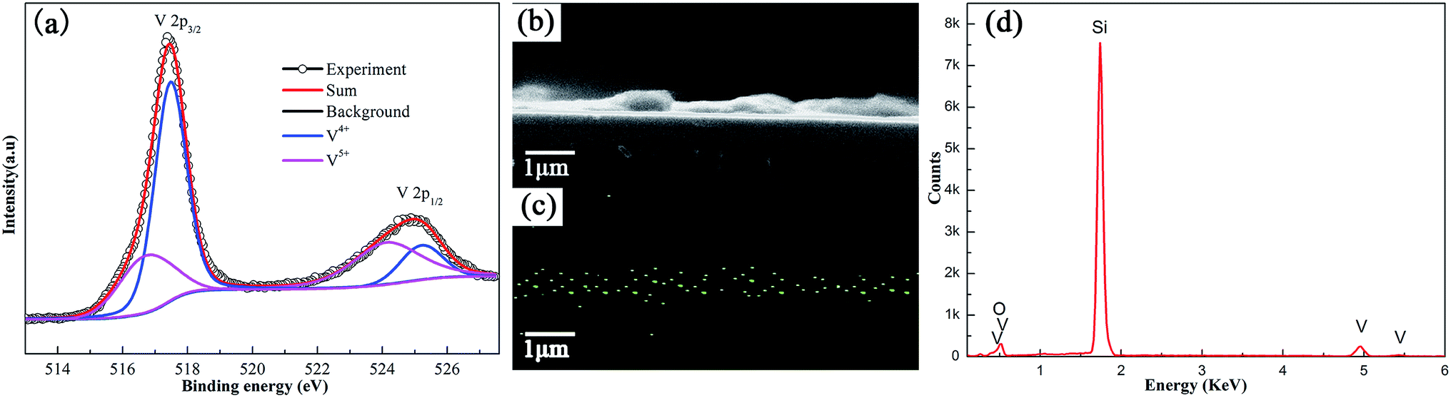
XPS was used to investigate composition of the V2Ox thin film with the optimal molar ratio of V2O5 to H2O2. High resolution XPS spectrum corresponding to V is shown in Fig. 1a. As shown in the images, the V 2p spectrum can be well fitted with 2p1/2 and 2p3/2 doublets by a Gaussian function, which corresponds to vanadium in two different oxidation states (V5+ and V4+). Two peaks at the binding energy (BE) of 517.7 and 525.1 eV are corresponding to the 2p doublet of V5+. And the other two peaks at the BE of 516.7 and 524.1 eV are correspond to the 2p doublet of V4+ respectively. The atomic concentration ratio of V5+ to V4+ is about 1.41:1 according to the area ratio of their peaks, implying that ∼41.5% V4+ exists in the V2Ox film layer. The V4+ ions in V2Ox film could result in the enhancement of conductivity of the HTL,51 which facilitates the transport and collection of charge carrier in the PSC. EDS can qualitatively and quantitatively analyze all elements of the sample. The V2Ox solution is spin-coated on the polished monocrystalline silicon wafer rather than the ITO coated glass. The reason is that wafers have a lower roughness compared with the ITO film surface, which helps observe clearly the cross-section image of V2Ox film. As shown in Fig. 1b–d, the cross-section FESEM image together with vanadium elemental mapping and EDS spectrum are performed on V2Ox film based on monocrystalline silicon. The signals of V content of V2Ox film material were clearly observed. Moreover, it is important for us to point out that peaks of 2p1/2 and 2p3/2 coral electron are also clearly identified at 524.9 and 517.5 eV respectively in the XPS spectrum of the V2Ox film.
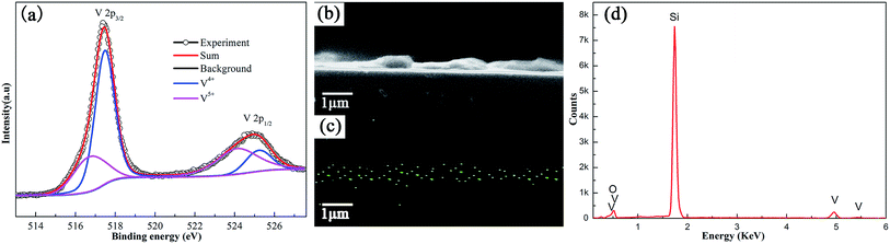 |
| | Fig. 1 (a) The high resolution XPS spectrum corresponding to V in V2Ox film. The cross-section FESEM image (b), mapping (c) and EDS spectrum (d) for V elemental of V2Ox film based on monocrystalline silicon. | |
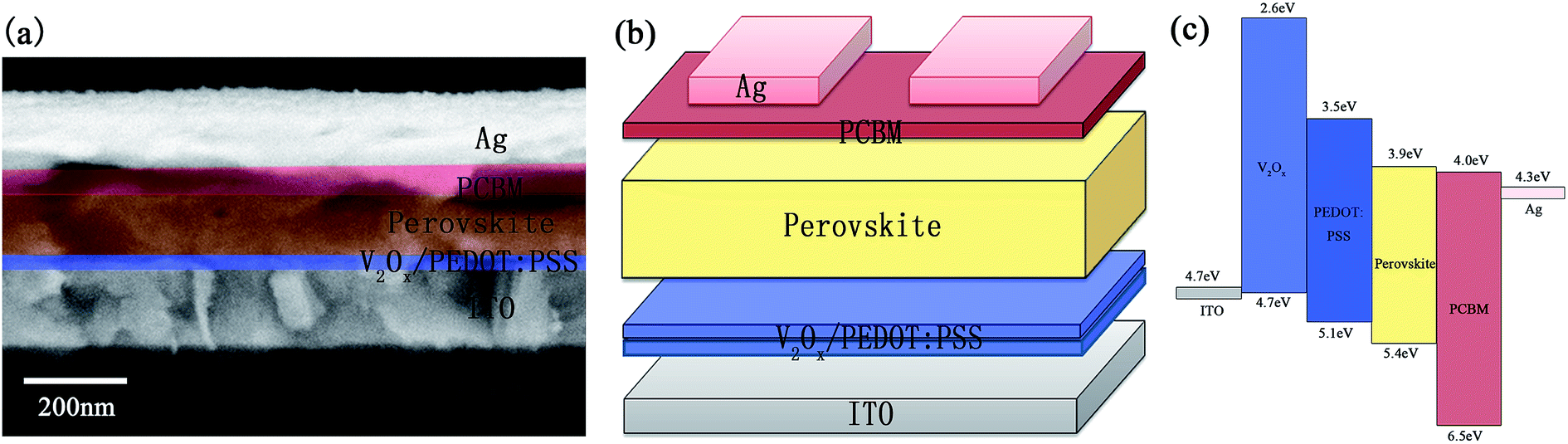
Fig. 2a and b show the schematic illustration and associated cross-section FESEM image of the prepared inverted PHJ PSC device with the structure of ITO/V2Ox/PEDOT:PSS/CH3NH3PbI3−xClx/PCBM/Ag. The double-decked V2Ox/PEDOT:PSS thin film (∼40 nm) is used as the HTL on the ITO bottom electrode (∼200 nm) of PSC device. CH3NH3PbI3−xClx film (∼250 nm) is chosen as photoactive layer, PCBM film (∼45 nm) as ETL and Ag film (∼150 nm) as top electrode. The energy level diagram corresponding to each layer of the PSC has been shown in Fig. 2c. As shown in Fig. S1,† the WF of V2Ox films are examined by UPS, and related values of ITO, PEDOT:PSS, PCBM and Ag are also given in previous studies.52 The WF of V2Ox (4.74 eV) is lower than that of PEDOT:PSS (5.10 eV),39 which could lead to the rise in short-circuit current density (JSC), enhancement the extraction of the charge carriers from the absorption layer and reduction the carriers recombination.
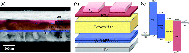 |
| | Fig. 2 The cross-section FESEM image (a), the schematic illustration (b) and the energy level diagram (c) of the PSC device with double-decked V2Ox/PEDOT:PSS film. | |
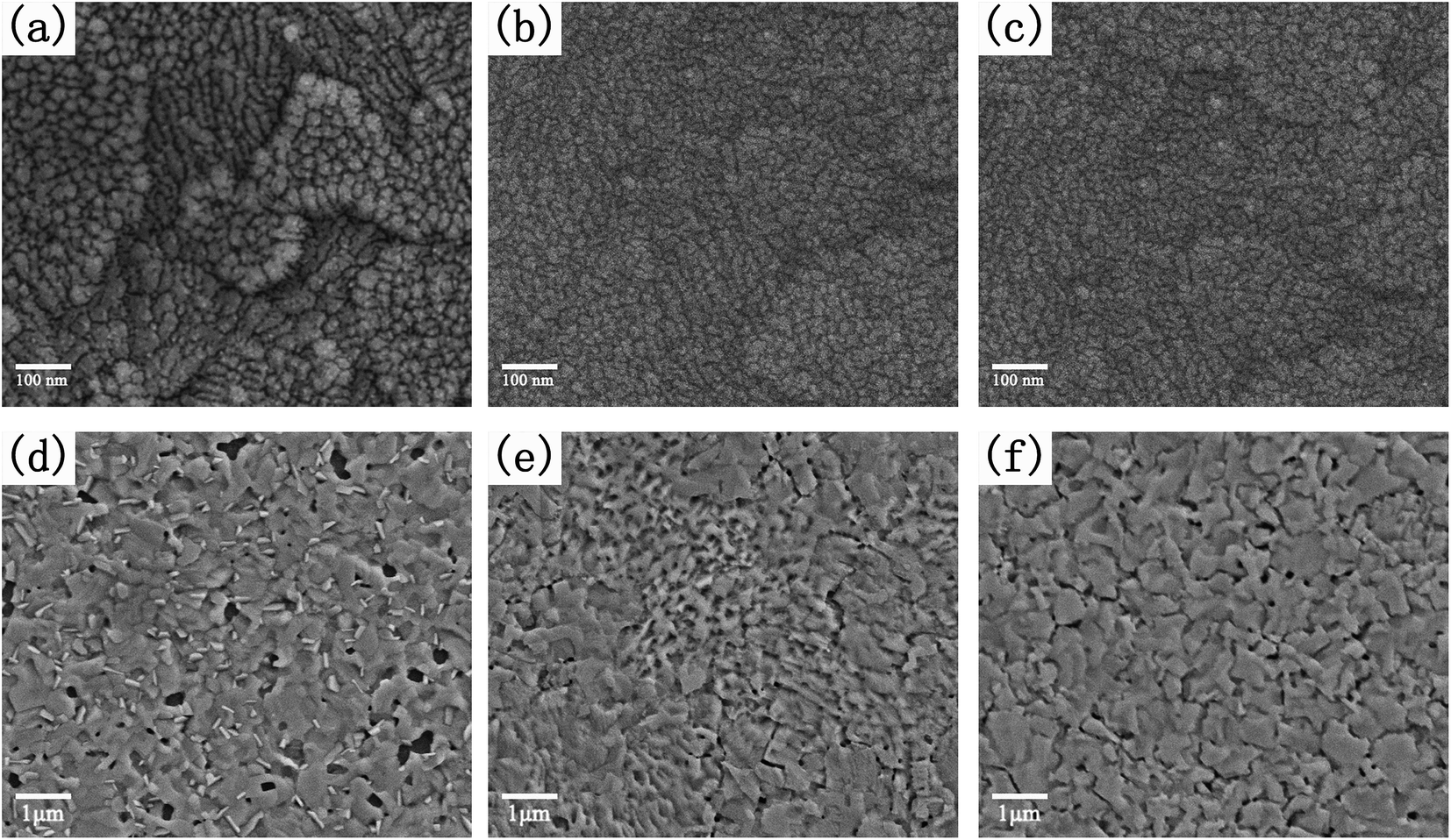
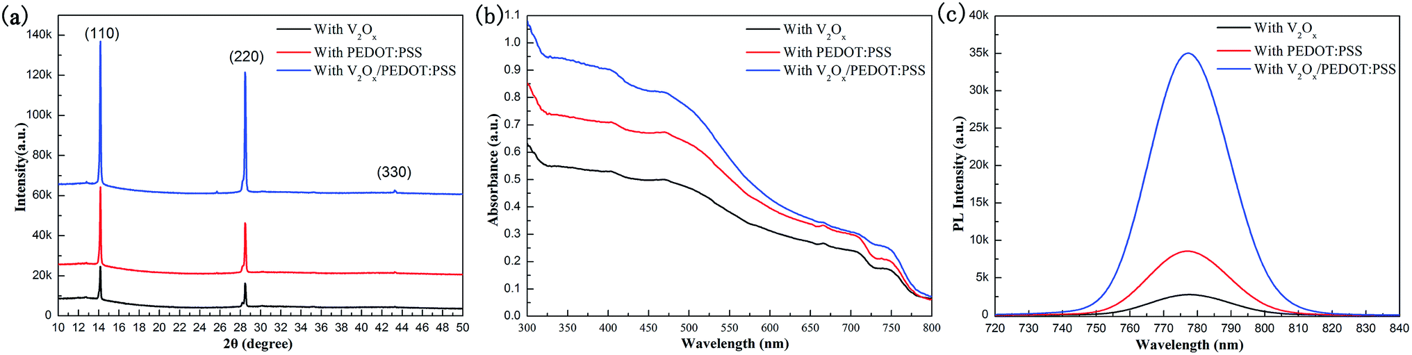
In order to analyze the effect of different HTL films on the crystallization of CH3NH3PbI3−xClx thin films, we have measured the FESEM images of various HTL films and perovskite thin films based on HTL films. The surface FESEM images of V2Ox, PEDOT:PSS and V2Ox/PEDOT:PSS HTL films based on ITO coated glasses are shown in Fig. 3a–c, respectively. It is found that some particles with different sizes (the diameter ranges from 10 nm to 30 mm) are presented on surface of the V2Ox film. The surfaces of ITO/PEDOT:PSS and ITO/V2Ox/PEDOT:PSS films are more smooth than that of V2Ox film, which will be more conducive to the growth of CH3NH3PbI3−xClx films. The AFM images of V2Ox, PEDOT:PSS and V2Ox/PEDOT:PSS HTL films are shown in Fig. S2a–c.† The surface roughness (root-mean-square, RMS) values of the V2Ox, PEDOT:PSS and the V2Ox/PEDOT:PSS HTL films are ∼5.7 nm, ∼3.3 nm and ∼2.5 nm, respectively. Compared with conventional PEDOT:PSS films, the V2Ox/PEDOT:PSS film has a lower roughness. The roughness of the HTL film has a great influence on the morphology of perovskite films. Fig. 3d–f show surface FESEM images of CH3NH3PbI3−xClx thin films based on ITO/V2Ox, ITO/PEDOT:PSS and ITO/V2Ox/PEDOT:PSS films respectively. The V2Ox film with different sizes of particles might be detrimental to the formation of crystal nucleus sites and the growth of crystalline grains, resulting in larger pores (the diameter of pores ranges from 50 nm to 300 mm) on the perovskite film surface based on ITO/V2Ox. On the contrary, the pores of perovskite film based on ITO/PEDOT:PSS or ITO/V2Ox/PEDOT:PSS are fewer and smaller, with the diameter of less than 50 nm. Furthermore, compared with the other two perovskite films, the film based on ITO/V2Ox/PEDOT:PSS shows a larger crystal grains and more uniform surface topography, which results from the smoother V2Ox/PEDOT:PSS HTL film (Fig. S2†). This is consistent with the results presented in the XRD pattern (Fig. 4a). The XRD analysis of CH3NH3PbI3−xClx films shows diffraction peaks at 14.22°, 28.56°, and 43.29°, corresponding to (110), (220), and (330) planes, respectively. The lattice parameters of CH3NH3PbI3−xClx films with tetragonal perovskite structure are a = 8.825 Å, b = 8.835 Å and c = 11.24 Å, similar to that of CH3NH3PbI3 previously reported.10,44 Probably, the weak diffraction peaks of PbI2 appear at 12.77° and 25.71°, because CH3NH3PbI3−xClx film is decomposed into a little PbI2 under the condition of prolonged annealing. Obviously, compared with other two perovskite films, CH3NH3PbI3−xClx thin film with double-decked V2Ox/PEDOT:PSS film has a better crystallinity, which is in alignment with the FESEM images (Fig. 3d–f). The UV/Vis absorption spectra of the CH3NH3PbI3−xClx films spin-coated on the different HTLs are shown in Fig. 4b. The perovskite film with double-decked V2Ox/PEDOT:PSS layer has a stronger absorption within the ranges of 300–800 nm, compared with other two perovskite films. In order to further confirm performances of the HTLs serving as charge acceptors within the PSCs, steady-state PL measurements were carried out to investigate the quenching of perovskite emission. The quenching of the PL emission by the V2Ox, PEDOT:PSS and V2Ox/PEDOT:PSS layers can be clearly observed in Fig. 4c. The steady-state PL response clearly shows that the CH3NH3PbI3−xClx films with HTLs appear a PL intensity peak at about 780 nm. It should be noted that the PL intensity of CH3NH3PbI3−xClx film with double-decked V2Ox/PEDOT:PSS layer is the lowest. This indicates that the double-decked V2Ox/PEDOT:PSS film plays an important role in quenching recombination channels of electrons and holes in PSC devices.
 |
| | Fig. 3 The surface FESEM images of V2Ox film (a), PEDOT:PSS film (b) and V2Ox/PEDOT:PSS HTL film (c) based on ITO coated glasses. The surface FESEM images of CH3NH3PbI3−xClx thin films based on ITO/V2Ox (d), ITO/PEDOT:PSS (e) and ITO/V2Ox/PEDOT:PSS films (f), respectively. | |
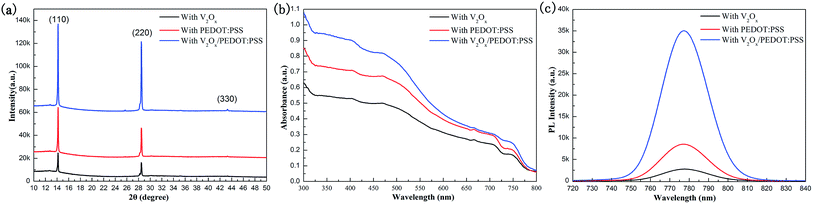 |
| | Fig. 4 The XRD spectra (a), the absorbance spectra (b) and the steady-state PL spectra (c) of the CH3NH3PbI3−xClx films after being annealed on the V2Ox film, the pristine PEDOT:PSS film, and the double-decked V2Ox/PEDOT:PSS composite film, respectively. | |
3.2 The photovoltaic performance of PSCs
In order to compare the properties of different HTL materials, we fabricate three kinds of PSC devices with PEDOT:PSS, V2Ox/PEDOT:PSS and PEDOT:PSS/V2Ox HTL films. The photoelectric properties of three PSCs are measured under the illumination of AM 1.5 G simulated solar light at 100 mW cm−2. The J–V curves of the PSC devices are shown in Fig. 5a. In our study, a conventional inverted PHJ PSC device with PEDOT:PSS HTL film is used as reference device. For the device with double-decked PEDOT:PSS/V2Ox film, although the VOC of it has been improved, its JSC and FF are lowered notably, resulting in its lower PCE. With the bias voltage increase, the current density experiences the process: slight decline—slight increase—rapid decline (Fig. 5a). For this strange phenomenon, we have not found a reasonable explanation. A explanation might be that oxygen deficiencies close to the Fermi level of the material and reduction in doping in the perovskite film,53,54 result in the increase of current in the process of applying forward bias to PSC device with double-decked PEDOT:PSS/V2Ox film. Compared with reference device, the performances of PSC device with double-decked V2Ox/PEDOT:PSS film have been significantly improved, such as the open circuit voltage (VOC), JSC, fill factor (FF) and PCE. The uniform and dense morphology of the perovskite film with double-decked V2Ox/PEDOT:PSS film (Fig. 3f) can effectively avoid defects and achieve a better performance.
 |
| | Fig. 5 The J–V curves (a), the dark J–V curves (b) and the EIS spectra with the equivalent circuit (c) of PSCs based on the V2Ox film, the pristine PEDOT:PSS film, and the double-decked V2Ox/PEDOT:PSS composite film, respectively. | |
To further understand the mechanism of performance improvement of PSCs with the double-decked V2Ox/PEDOT:PSS HTL, the J–V curves (Fig. 5b) of three devices are recorded in the dark conditions. Dark current measurement is an effective method of evaluating the recombination of free carriers and charge carrier loss in the leakage pathways.55 It can be shown that the double-decked V2Ox/PEDOT:PSS and PEDOT:PSS/V2Ox could simultaneously prevent the leakage current under the condition of reverse bias and improve the current injection under the forward bias. Obviously, the smallest leakage current density and the largest rectification ratio are presented in the dark J–V curve of the device with double-decked V2Ox/PEDOT:PSS at reverse-biased region, indicating a desired diode characteristics.56 EIS measurements are performed to analyze the interfacial charge transfer process of devices. The Nyquist plots of three devices with different HTLs are shown in Fig. 5c. The frequency range measured is from 106 to 1 Hz with AC amplitude of 10 mV at 0.84 V bias. Each impedance spectra is simulated through an equivalent circuit, forming a semicircle. The photovoltaic parameters of the devices are shown in Table 1, including series resistance (Rs), parallel resistance (Rp) and capacitance (C). It is found that C is similar among three devices with different HTLs while their Rp are changed regularly. The resistance of charge transport of the device with double-decked V2Ox/PEDOT:PSS film is the lowest. This indicates that charge transport rate of the device with double-decked V2Ox/PEDOT:PSS HTL film is the biggest among devices in this study.
Table 1 The photovoltaic parameters of the PSC devices with different HTLs
| Devices |
Rs (Ω) |
Rp (kΩ) |
C (nF) |
| With PEDOT:PSS |
39.91 |
18.87 |
6.25 |
| With V2Ox/PEDOT:PSS |
43.17 |
13.08 |
7.36 |
| With PEDOT:PSS/V2Ox |
336.89 |
43.17 |
7.61 |
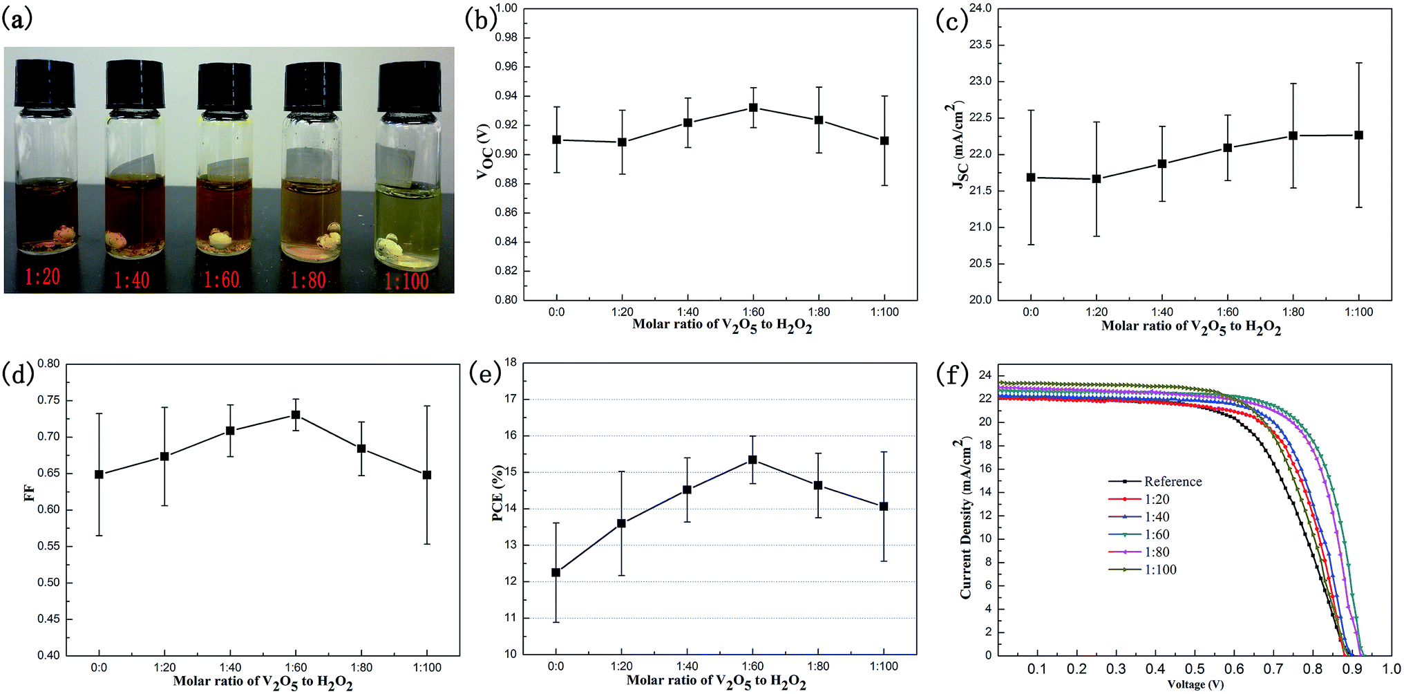
The valence state of the vanadium element in the vanadium oxide has exerted a great influence on the conductivity of the HTL thin film and photoelectric properties of the PSC device. In our study, we change the valence of vanadium in the V2Ox by adjusting the molar ratio (1:20, 1:40, 1:60, 1:80 and 1:100) of V2O5 to H2O2. The photograph of various V2Ox solutions is shown in Fig. 6a. As the proportion of H2O2 increases, the color of the V2Ox solution gradually becomes light. The contents of V4+ and V4+ of the V2Ox thin film measured by XPS are shown in Table 2. The content of V4+ increases with the ratio of H2O2, resulting in a higher conductivity of the double-decked V2Ox/PEDOT:PSS HTL film. As shown in Fig. 6b–e, the mean and standard deviations of the VOC, JSC, FF and PCE of PSC devices with different molar ratios of H2O2 to V2O5 are calculated. It is found that the JSC increases with molar ratio of H2O2 to V2O5. The conductivity of the double-decked V2Ox/PEDOT:PSS HTL film improves with the increase of V4+, thus the JSC of the device increases. However, the VOC, FF and PCE show a trend—increase and then decline. Possibly, the decline of V5+ results in less doping and more defects of V2Ox thin film, as well as a lower performance of device. The best-performance (Fig. 6f) and high-reproducibility device is achieved when the molar ratio of V2O5 to H2O2 is 1:60, namely, the content of V4+ is 41.5%.
 |
| | Fig. 6 (a) The photograph of the V2Ox solution prepared by mixing V2O5 and H2O2 at different molar ratios (1:20, 1:40, 1:60, 1:80 and 1:100). The mean and standard deviations of the VOC (b), JSC (c), FF (d) and PCE (e), and the J–V curves (f) of the PSC devices with double-decked V2Ox/PEDOT:PSS HTL film with different molar ratios of H2O2 to V2O5. | |
Table 2 The valence state contents of the V element of V2Ox thin film with different molar ratios of V2O5 to H2O2
| V element |
Molar ratios of V2O5 to H2O2 |
| 1:20 |
1:40 |
1:60 |
1:80 |
1:100 |
| V4+ |
33.52% |
38.13% |
41.47% |
43.97% |
45.38% |
| V5+ |
66.48% |
61.87% |
58.53% |
56.03% |
54.62% |
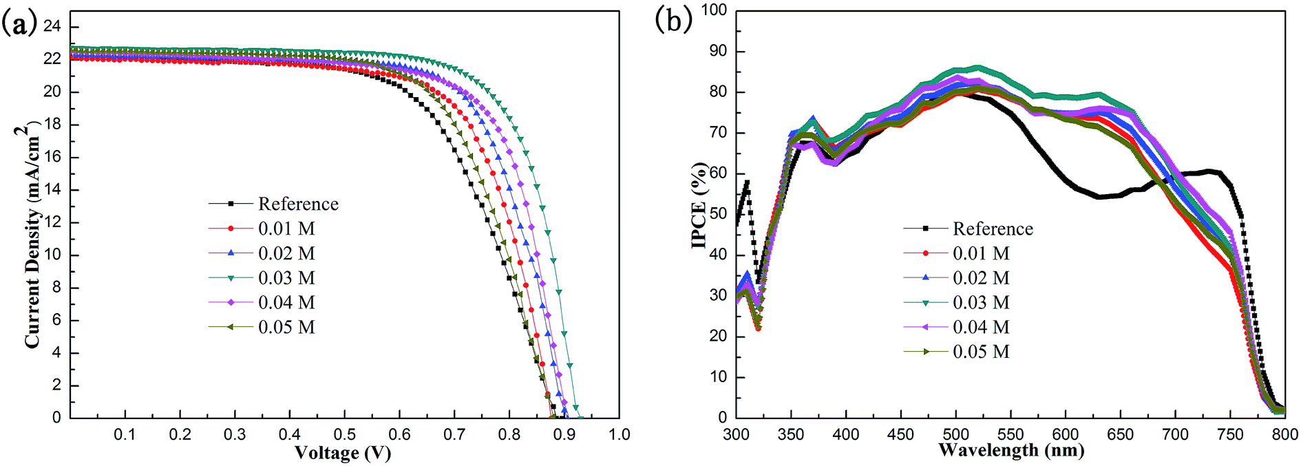
The concentration of V2Ox solution has a great influence on the thickness and uniformity of the double-decked V2Ox/PEDOT:PSS HTL film. Therefore, we prepare V2Ox solutions with different concentration gradients (0.01, 0.02, 0.03, 0.04 and 0.05 M). The J–V characteristics of PSC based on pristine PEDOT:PSS and double-decked V2Ox/PEDOT:PSS HTL film with varied concentration of V2Ox solution are shown in Fig. 7a. The Table 3 shows the key performance parameters of PSCs, including VOC, JSC, FF and PCE. The best performance of device is achieved under the concentration of 0.03 M of V2Ox solutions. With the increase of concentration of the V2Ox solution, all performance parameters of devices show a trend, that is, increase first and then decrease, except JSC. The reason why JSC keeps rising is that a higher concentration of V2Ox solution allows the V2Ox film to have a larger contact area with the PEDOT:PSS film. The thickness of the double-decked V2Ox/PEDOT:PSS HTL film increases with concentration of V2Ox solution. On the one hand, when the concentration of V2Ox solution is very low, the V2Ox particles excessively disperse, failing to form the film. On the other hand, when the concentration of V2Ox solution gets very high, the film has a higher roughness. Moreover, there is a large barrier to extraction through the metal oxide valence band, because the V2Ox/PEDOT:PSS layer is too thick to allow the tunnelling of charges. There is no doubt that these two aspects of the factors are not conducive to preparing high-performance devices. Fig. 7b shows the IPCE spectra of the PSCs based on pristine PEDOT:PSS and double-decked V2Ox/PEDOT:PSS HTL film. Compared with the conventional AM 1.5 solar radiation spectrum,57 interestingly, the IPCE of devices based on V2Ox/PEDOT:PSS increases within a wide wavelength range between 500 and 700 nm, indicating that the devices with double-decked V2Ox/PEDOT:PSS HTL can absorb more solar energy and convert it into electrical energy. In particular, the performance of the device with 0.03 M V2Ox is the best among devices.
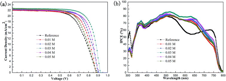 |
| | Fig. 7 The J–V curves (a) and IPCE spectra (b) of PSC based on pristine PEDOT:PSS and double-decked V2Ox/PEDOT:PSS HTL film with varied-concentration V2Ox solution (0.01, 0.02, 0.03, 0.04 and 0.05 M). | |
Table 3 The main performance parameters of PSCs with varied concentration of V2Ox solution
| Devices |
VOC (V) |
JSC (mA cm−2) |
FF |
PCE (%) |
| Reference |
0.92(0.91 ± 0.03) |
22.25(21.26 ± 1.07) |
0.72(0.67 ± 0.07) |
13.56(11.85 ± 1.81) |
| 0.01 M |
0.93(0.92 ± 0.02) |
22.15(21.23 ± 0.98) |
0.72(0.68 ± 0.06) |
14.95 (13.53 ± 1.75) |
| 0.02 M |
0.94(0.93 ± 0.02) |
22.19(21.57 ± 0.75) |
0.73(0.71 ± 0.03) |
15.32(14.17 ± 1.17) |
| 0.03 M |
0.94(0.93 ± 0.01) |
22.41(21.96 ± 0.51) |
0.75(0.74 ± 0.02) |
15.86(14.97 ± 0.91) |
| 0.04 M |
0.93(0.92 ± 0.01) |
22.63(21.97 ± 0.89) |
0.74(0.73 ± 0.03) |
15.67(14.75 ± 0.99) |
| 0.05 M |
0.93(0.91 ± 0.04) |
23.12(21.99 ± 1.19) |
0.74(0.66 ± 0.09) |
15.18(13.98 ± 1.69) |
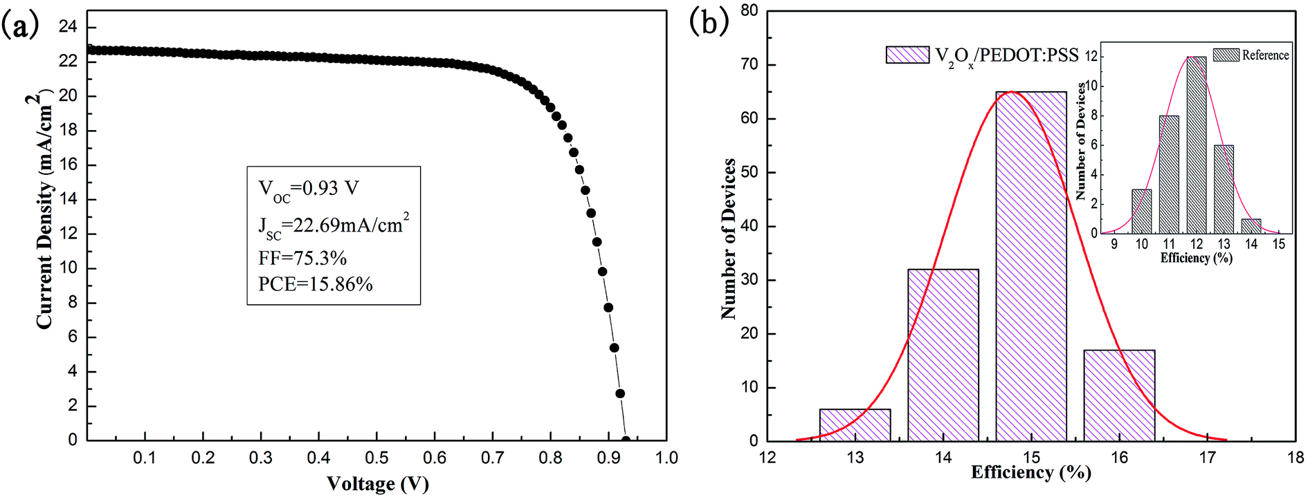
The best performance of PSC device is achieved by controlling the optimal molar ratio of V2O5 to H2O2 and the concentration of the V2Ox solution. The J–V curve and main parameters (VOC, JSC, FF and PCE) of the best-performance device with the double-decked V2Ox/PEDOT:PSS HTL film are shown in Fig. 8a. A best PCE of 15.86%, corresponding to a JSC of 22.69 mA cm−2, a VOC of 0.93 V, and a FF of 0.75, is achieved. In our study, as shown in the histograms of PCE parameters of reference devices with PEDOT:PSS HTL (30 cells) (inset) and controllable devices with the double-decked V2Ox/PEDOT:PSS HTL (120 cells) (Fig. 8b), the devices performance follows a Gaussian distribution and achieves the PCEAVE of 11.85% and 14.97% respectively. The relative standard deviations of the reference devices and devices based on the V2Ox/PEDOT:PSS are 9.8% and 4.5%, respectively, indicating that the latter shows a better reproducibility than the former.
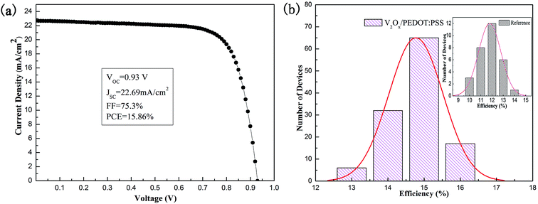 |
| | Fig. 8 (a) The J–V curve and main parameters of the best-performance device with the double-decked V2Ox/PEDOT:PSS HTL film. (b) The histogram of PCEs of 120 double-decked V2Ox/PEDOT:PSS HTL controlled devices. Inset is the histogram of PCEs of 30 reference devices with PEDOT:PSS HTL. (Gaussian distributions were fit to obtain the average and relative standard deviations.) | |
4. Conclusions
With hard efforts we have successfully used solution-processed double-decked V2Ox/PEDOT:PSS film as HTL of high-performance inverted planar PSCs. In our study, the best performance of the devices has been achieved by changing the valence of vanadium of double-decked V2Ox/PEDOT:PSS film. Furthermore, the device performance has been optimized by controlling the optimum concentration of the V2Ox solution. The results show that the double-decked V2Ox/PEDOT:PSS film plays an essential role in improving charge transfer rate and suppressing the electron–hole pair recombination. With this double-decked film, the PCE and reproducibility of PSCs have been improved significantly.
Acknowledgements
The authors gratefully acknowledge financial support from Natural Science Foundation of China (NSFC Grant No. 51502081), Doctoral Research Fund of Henan Normal University (No. 5101029170256), Science Funds for Young Scholar of Henan Normal University (No. 5101029279082).
Notes and references
- M. Grätzel, Nat. Mater., 2014, 13, 838–842 CrossRef PubMed.
- N. G. Park and J. Phys, Chem. Lett., 2013, 4, 2423–2429 CAS.
- T. Baikie, Y. Fang, J. M. Kadro, M. Schreyer, F. X. Wei, S. G. Mhaisalkar, M. Graetzel and T. J. White, J. Mater. Chem. A, 2013, 1, 5628–5641 CAS.
- G. C. Xing, N. Mathews, S. Y. Sun, S. S. Lim, Y. M. Lam, M. Grätzel, S. Mhaisalkar and T. C. Sum, Science, 2013, 342, 344–347 CrossRef CAS PubMed.
- S. D. Stranks, G. E. Eperon, G. Grancini, C. Menelaou, M. J. P. Alcocer, T. Leijtens, L. M. Herz, A. Petrozza and H. J. Snaith, Science, 2013, 342, 341–344 CrossRef CAS PubMed.
- W. Nie, H. Tsai, R. Asadpour, J. C. Blancon, A. J. Neukirch, G. Gupta, J. J. Crochet, M. Chhowalla, S. Tretiak and M. A. Alam, Science, 2015, 347, 522–525 CrossRef CAS PubMed.
- G. E. Eperon, V. M. Burlakov, P. Docampo, A. Goriely and H. J. Snaith, Adv. Funct. Mater., 2014, 24, 151–157 CrossRef CAS.
- B. Conings, L. Baeten, C. D. Dobbelaere, J. D'Haen, J. Manca and H. G. Boyen, Adv. Mater., 2014, 26, 2041–2046 CrossRef CAS PubMed.
- C. G. Wu, C. H. Chiang, Z. L. Tseng, M. K. Nazeeruddin, A. Hagfeldt and M. Grätzel, Energy Environ. Sci., 2015, 8, 2725–2733 CAS.
- A. Kojima, K. Teshima, Y. Shirai and T. Miyasaka, J. Am. Chem. Soc., 2009, 131, 6050–6051 CrossRef CAS PubMed.
- NREL, http://www.nrel.gov/ncpv/images/efficiency_chart.jpg, accessed 10 April 2016.
- W. Ke, D. Zhao, C. R. Grice, A. J. Cimaroli, J. Ge, H. Tao, H. Lei, G. Fang and Y. Yan, J. Mater. Chem. A, 2015, 3, 17971–17976 CAS.
- M. Qian, M. Li, X. Shi, H. Ma, Z. K. Wang and L. Liao, J. Mater. Chem. A, 2015, 3, 13533–13539 CAS.
- Q. Chen, H. Zhou, Z. Hong, S. Luo, H. S. Duan, H. H. Wang, Y. Liu, G. Li and Y. Yang, J. Am. Chem. Soc., 2013, 136, 622–625 CrossRef PubMed.
- D. Liu and T. L. Kelly, Nat. Photonics, 2014, 8, 133–138 CrossRef CAS.
- H. S. Kim, C. R. Lee, J. H. Im, K. B. Lee, T. Moehl, A. Marchioro, S. J. Moon, R. Humphry-Baker, J. H. Yum, J. E. Moser, M. Grätzel and N. G. Park, Sci. Rep., 2012, 2, 591–597 Search PubMed.
- F. Zuo, S. T. Williams, P. W. Liang, C. C. Chueh, C. Y. Liao and A. K. Y. Jen, Adv. Mater., 2014, 26, 6454–6460 CrossRef CAS PubMed.
- M. A. Green, A. Ho-Baillie and H. J. Snaith, Nat. Photonics, 2014, 8, 506–514 CrossRef CAS.
- Y. C. Shao, Z. G. Xiao, C. Bi, Y. B. Yuan and J. S. Huang, Nat. Commun., 2014, 5, 5784–5790 CrossRef CAS PubMed.
- C. Zuo and L. Ding, Nanoscale, 2014, 6, 9935–9938 RSC.
- Z. Xiao, Q. Dong, C. Bi, Y. Shao, Y. Yuan and J. Huang, Adv. Mater., 2014, 26, 6503–6509 CrossRef CAS PubMed.
- J. Seo, S. Park, Y. C. Kim, N. J. Jeon, J. H. Noh, S. C. Yoon and S. I. Seok, Energy Environ. Sci., 2014, 7, 2642–2646 CAS.
- S. W. Tong, C. F. Zhang, C. Y. Jiang, G. Liu, Q. D. Ling, E. T. Kang, D. S. H. Chan and C. X. Zhu, Chem. Phys. Lett., 2008, 453, 73–76 CrossRef CAS.
- S. Jönsson, J. Birgerson, X. Crispin, G. Greczynski, W. Osikowicz, A. W. Denier van der Gon, W. R. Salaneck and M. Fahlman, Synth. Met., 2013, 139, 1–10 CrossRef.
- Y. H. Kim, C. Sachse, M. L. Machala, C. May, L. Müller-Meskamp and K. Leo, Adv. Funct. Mater., 2011, 21, 1076–1081 CrossRef CAS.
- J. H. Kim, P. W. Liang, S. T. Williams, N. Cho, C. C. Chueh, M. S. Glaz, D. S. Ginger and A. K. Y. Ken, Adv. Mater., 2015, 27, 695–701 CrossRef CAS PubMed.
- J. Y. Jeng, K. C. Chenk, T. Y. Chiang, P. Y. Lin, T. D. Tsai, Y. C. Chang, T. F. Guo, P. Chen, T. C. Wen and Y. J. Hsu, Adv. Mater., 2014, 26, 4107–4113 CrossRef CAS PubMed.
- J. Cui, F. Meng, H. Zhang, K. Cao, H. Yuan, Y. Cheng, F. Huang and M. Wang, ACS Appl. Mater. Interfaces, 2014, 6, 22862–22870 CAS.
- Z. Zhu, Y. Bai, T. Zhang, Z. Liu, X. Long, Z. Wei, Z. Wang, L. Zhang, J. Wang, F. Yan and S. Yang, Angew. Chem., Int. Ed., 2014, 53, 12571–12783 CAS.
- L. Hu, W. Wang, H. Liu, J. Peng, H. Cao, G. Shao, Z. Xie, W. Ma and J. Tang, J. Mater. Chem. A, 2015, 3, 515–518 CAS.
- V. Shrotriya, G. Li, Y. Yao, C. W. Chu and Y. Yang, Appl. Phys. Lett., 2006, 88, 73508–73510 CrossRef.
- I. Hancox, K. V. Chauhan, P. Sullivan, R. A. Hatton, A. Moshar, C. P. A. Mulcahy and T. S. Jones, Energy Environ. Sci., 2010, 3, 107–110 CAS.
- D. Y. Kim, J. Subbiah, G. Sarasqueta, F. So, H. Ding, Irfan and Y. Gao, Appl. Phys. Lett., 2009, 95, 93304–93308 CrossRef.
- A. K. K. Kyaw, X. W. Sun, C. Y. Jiang, G. Q. Lo, D. W. Zhao and D. L. Kwong, Appl. Phys. Lett., 2008, 93, 221107–221109 CrossRef.
- F. C. Krebs, Sol. Energy Mater. Sol. Cells, 2009, 93, 465–475 CrossRef CAS.
- O. Hagemann, M. Bjerring, N. C. Nielsen and F. C. Krebs, Sol. Energy Mater. Sol. Cells, 2008, 92, 1327–1335 CrossRef CAS.
- D. Y. Lee, S. I. Na and S. S. Kim, Nanoscale, 2016, 8, 1513–1522 RSC.
- F. Hou, Z. Su, F. Jin, X. Yan, L. Wang, H. Zhao, J. Zhu, B. Chu and W. Li, Nanoscale, 2015, 7, 9427–9432 RSC.
- H. Peng, W. Sun, Y. Li, S. Ye, H. Rao, W. Yan, H. Zhou, Z. Bian and C. Huang, Nano Res., 2016, 9, 2960–2971 CrossRef CAS.
- J. Liu, Q. Li, T. Wang, D. Yu and Y. Li, Angew. Chem., 2004, 116, 5158–5162 CrossRef.
- H. Phetmung, T. W. Kim, S. J. Hwang and J. H. Choy, J. Iran. Chem. Soc., 2008, 5, 706–711 CrossRef CAS.
- X. Wu, Y. Tao, L. Dong and J. Hong, J. Mater. Chem., 2004, 14, 901–904 RSC.
- Y. Liu, M. Bag, L. A. Renna, Z. A. Page, P. Kim, T. Emrick, D. Venkataraman and T. P. Russell, Adv. Energy Mater., 2016, 6, 1501606–1501612 CrossRef.
- M. M. Lee, J. Teuscher, T. Miyasaka, T. N. Murakami and H. J. Snaith, Science, 2012, 338, 643–647 CrossRef CAS PubMed.
- Z. Liu, T. He, H. Wang, X. Song, H. Liu, J. Yang, K. Liu and H. Ma, RSC Adv., 2017, 7, 18456–18465 RSC.
- M. Saliba, T. K. Wee, S. Hiroaki, D. T. Moore, S. Trent, W. Zhang, L. A. Estroff, W. Ulrich and H. J. Snaith, J. Phys. Chem. C, 2014, 118, 17171–17177 CAS.
- H. L. Hsu, C. P. Chen, J. Y. Chang, Y. Y. Yu and Y. K. Shen, Nanoscale, 2014, 6, 10281–10288 RSC.
- S. Bai, Z. W. Wu, X. J. Wu, Y. Z. Jin, N. Zhao, Z. H. Chen, Q. Q. Mei, X. Wang, Z. Z. Ye and T. Song, Nano Res., 2014, 12, 1749–1758 CrossRef.
- M. Schindler, F. C. Hawthorne and W. H. Baur, Chem. Mater., 2000, 12, 1248–1259 CrossRef CAS.
- L. Pettersson, I. Andersson and A. Gorzsás, Coord. Chem. Rev., 2003, 237, 77–87 CrossRef CAS.
- D. Manno, A. Serra, M. Di Giulio, G. Micocci, A. Taurino, A. Tepore and D. Berti, J. Appl. Phys., 1997, 81, 2709–2714 CrossRef CAS.
- J. Y. Jeng, Y. F. Chiang, M. H. Lee, S. R. Peng, T. F. Guo, P. Chen and T. C. Wen, Adv. Mater., 2013, 25, 3727–3732 CrossRef CAS PubMed.
- K. Kanai, K. Koizumi, S. Ouchi, Y. Tsukamoto, K. Sakanoue, Y. Ouchi and K. Seki, Org. Electron., 2010, 11, 188–194 CrossRef CAS.
- M. Vasilopoulou, L. C. Palilis, D. G. Georgiadou, A.
M. Douvas, P. Argitis, S. Kennou, L. Sygellou, G. Papadimitropoulos, I. Kostis, N. A. Stathopoulos and D. Davazoglou, Adv. Funct. Mater., 2011, 21, 1489–1497 CrossRef CAS.
- K. Sun, J. Chang, F. H. Isikgor, P. Li and J. Ouyang, Nanoscale, 2015, 7, 896–900 RSC.
- C. He, C. Zhong, H. Wu, R. Yang, W. Yang, F. Huang, G. C. Bazan and Y. Cao, J. Mater. Chem., 2010, 20, 2617–2622 RSC.
- GB/T 17683.1-1999, Solar energy-reference solar spectral irradiance at the ground at different receiving conditions-part 1: direct normal and hemispherical solar irradiance for air mass 1.5.
Footnote |
| † Electronic supplementary information (ESI) available. See DOI: 10.1039/c7ra04414c |
|
| This journal is © The Royal Society of Chemistry 2017 |
Click here to see how this site uses Cookies. View our privacy policy here. 
 Open Access Article
 This Open Access Article is licensed under a Creative Commons Attribution-Non Commercial 3.0 Unported Licence
 *ab,
Tingwei Heab,
Kaikai Liua,
Qinqin Zhia and
Mingjian Yuan*abc
*ab,
Tingwei Heab,
Kaikai Liua,
Qinqin Zhia and
Mingjian Yuan*abc