
 Open Access Article
 This Open Access Article is licensed under a
 Creative Commons Attribution 3.0 Unported Licence
High-performance thermal sensitive VO2(B) thin films prepared by sputtering with TiO2(A) buffer layer and first-principles calculations study
Zhuohan Ding†
,
Yuanyuan Cui†,
Dongyun Wan*,
Hongjie Luo and
Yanfeng Gao *
*
School of Materials Science and Engineering, Shanghai University, Shanghai 200444, China. E-mail: yfgao@shu.edu.cn; echowandy@shu.edu.cn
First published on 6th June 2017
Abstract
VO2(B) is a candidate material for thermal sensors in uncooled infrared detectors; however, it suffers from low temperature coefficient of resistance (TCR) values and unfavorable square resistances. Here, we present an effective strategy to modify the electronic properties of VO2(B) by inducing elastic strain with an anatase TiO2(A) buffer layer. The combined experimental and first-principles computational study on TiO2(A)-induced VO2(B) thin films deposited by magnetron sputtering enables us to achieve high TCRs (−3.48% K−1) and favorable square resistances (18.97 kΩ). The underlying microscopic mechanism for the improvement in performance was studied, and the results indicate that the tensile strain contributes to a reduction in overlapping of V-3d orbitals and an increase in carrier concentrations along the c-axis in VO2(B), both of which result in an increase in the electrical conductivity and TCR values. These findings promote the design and fabrication of high-performance VO2(B) thin films by scaling the lattice strain along the c-axis with suitable buffer layers or substrates, and the simplicity of this method and the superior electrical properties of the films may enable its wide application in uncooled infrared detectors.
1. Introduction
Vanadium dioxide (VO2) is an abundant and polymorphous compound with fascinating thermal, electrical and optical properties.1–3 It has been reported that there are at least six polymorphs for VO2, among which the rutile VO2(R)4 and monoclinic VO2(M)5 phases are stable structures, while the tetragonal VO2(A),6 monoclinic VO2(B),7 monoclinic VO2(D)8 and paramontroseite VO2(P)9 are metastable phases. As we all know, VO2 must change its resistance with temperature, and the temperature coefficient of resistance (TCR) (β = (1/R)∂R/∂T) charactering such a change should be sufficiently high; here β is the TCR, R is the resistance and T is the temperature of VO2 film. VO2(M) previously was the most desired candidate for application in uncooled infrared (IR) detectors due to its strong semiconductor-to-metal transition (SMT) at 68 °C from the monoclinic phase (M phase) to the tetragonal rutile structure (R phase),1 and the consequent abrupt change of resistivity (a factor of 103–104) results in high TCR in the transition region.10 However, the maximum TCR value is only obtained in the high SMT temperature (TSMT) region, and the narrow temperature range for the high TCR values makes it unsuitable for use in practical devices. Moreover, the abrupt, first-order SMT is considered as a dilemma that needs to be avoided because a high nonlinearity is introduced in the sensing response. Although the nonstoichiometric, vanadium mixed oxide (VOx), which does not exhibit SMT and operates in a wide temperature range around room temperature, has also been employed in practical bolometric applications, the decrease in TSMT due to the presence of vacancies results in a significant decrease in TCR.11In comparison, VO2(B) exhibits potential as a unique thermal sensing material in uncooled IR detectors based on the absence of SMT properties,12 the absence of mutation of electrical or optical parameters, the absence of the thermal hysteresis phenomenon and the low 1/f noise at room temperature. Nevertheless, the low TCR value of VO2(B) (below −2.0% K−1) and its high resistivity at room temperature (R0) severely restrict its application in IR detectors.13–15
Many approaches have been considered to modify electronic properties of VO2(B) in our previous study such as doping16 and sandwich structure.17 Among them, the interfacial strain is also a very effective way to modify the electronic properties. It was reported that applying elastic strain to a semiconductor is an effective strategy for modifying its electronic properties.18,19 A typical approach for obtaining a strained semiconductor is by inducing the growth of the semiconductor on selected substrates by utilizing the lattice mismatch between the film and substrate. For instance, Yao et al. reported the growth of PrNiO3 thin films on SrTiO3, (LaAlO3)30(SrAlTaO6)70, and LaAlO3 single-crystal substrates with different lattice constants, and the nature of the lattice mismatch changed from compressive to tensile mismatch, with a corresponding reduction in the resistivity of PrNiO3.20 Li et al. demonstrated a highly effective strain for (111)-oriented GeSn thin films on Si substrate, which induced a direct band gap for high-performance optoelectronic materials.21
Very recently, Chen et al. reported the fabrication of textured VO2(B) thin films on SrTiO3 (001) planes through pulsed laser deposition and found tensile or compressive strains along the a-axis or b-axis; moreover, a small amount of VO2(M) was observed when the VO2(B) films grew thicker, and the thick films containing VO2(B) and VO2(M) exhibited a sharp semiconductor-to-metal transition.14 Motivated by these findings, we herein propose a strategy to tailor the electronic properties of VO2(B) by tuning the lattice strain along the c-axis, which is the direction of the corner-sharing VO6 octahedra.22 We expect that the sharing of electrons among the vanadium atoms along the [001] direction (c-axis) may result in stronger correlation effects among the electrons and the localization or delocalization of these correlation effects may have an impact on the electronic properties of VO2(B). Here, we focus on the anatase (A) TiO2 buffer layer to induce the growth of VO2(B). TiO2(A) is a tetragonal structure (space group I41/amd) with the lattice parameters aTiO2 = bTiO2 = 3.785 Å and cTiO2 = 9.514 Å,23 while VO2(B) is a monoclinic structure (space group C12/m1) with the lattice parameters aVO2 = 12.093 Å, bVO2 = 3.702 Å, and cVO2 = 6.433 Å.22 The relation between the VO2(B) phase and TiO2(A) substrate is defined as bTiO2 ≈ bVO2 and 2aTiO2 ≈ 1.2cVO2; thus, the growth of VO2(B) films on TiO2(A) substrates may result in a tensile strain along the c-axis of VO2(B).
In this study, by using the simple and feasible magnetron sputtering method, a TiO2(A) buffer layer was first deposited on the SiO2/Si substrate, then the growth of the VO2(B) was successfully induced with a 2.85% tensile strain along the c-axis by utilizing the lattice mismatch between the VO2(B) film and TiO2(A) buffer layer. The electronic performance of the strained VO2(B) thin film was clearly enhanced, as observed by the high TCR value (−3.48% K−1) and low square-resistance (18.97 kΩ), which are better than the values for the VO2(B) thin film directly deposited on the SiO2/Si substrate. Our first-principles calculations revealed that the tensile strain leads to reduced overlapping of the V-3d orbitals, which narrows the width of the V-3d band and makes the semiconductor VO2(B) more metallic, thus resulting in the increase in electrical conductivity. Moreover, the tensile strain along the c-axis increases the carrier concentrations in VO2, which results in the improvement in the electrical conductivity and the large TCR values obtained for VO2(B) under tensile strain.
2. Experimental procedures and calculation methods
2.1. Experimental procedures
The multi-layer films were deposited on silicon (SiO2/Si) and amorphous quartz substrates using a MSP3200 magnetron sputtering equipment with a 3-inch magnetron gun (USA GUN). RF sputtering of TiO2 and VO2 targets was used to deposit the TiO2 buffer layers and VO2 films, respectively. An un-throttled base pressure of 5 × 10⁻⁴ Pa was reached by a combined vacuum system, which included a mechanical pump and a turbomolecular pump. All of the sputtering experiments were carried out at nominal room temperature, under a working atmosphere of 30 sccm and a working pressure of 1.0 Pa. The TiO2 layers were deposited on substrates at an RF power of 160 W for 1200 s under the flow of a high-purity O2 gas (99.99%) and Ar gas (99.99%) mixture (1.0% O2 content), and then the films were annealed at 450 °C for 2 h in Ar atmosphere. The VO2 layers were subsequently deposited on the annealed TiO2 buffer layers at an RF power of 200 W for 900 s under the flow of pure argon. Finally, the as-deposited samples were annealed at different temperatures (from 350 °C to 500 °C) for 2 h in Ar atmosphere. For comparison, VO2 layers were also deposited directly onto the substrates, without the TiO2 buffer layers, under the same conditions.The crystallization patterns and phase structures of the films were clearly revealed by X-ray diffraction (XRD) measurements with monochromatized Cu-Kα source (λ = 1.5405 Å) operating at 40 kV and 40 mA in the range between 10° and 60° and grazing incidence X-ray diffraction (GIXRD) measurements with monochromatized Cu-Kα (λ = 1.5405 Å) radiation operating at 40 kV and 50 mA in the range between 10° and 80°. A Raman Renishaw RM3000 spectrometer with a 633 nm He–Ne laser was used to investigate chemical bonding between various elements and compounds. X-ray photoelectron spectroscopy (XPS) experiments were carried out on an ESCA 2000 system (VG Microtech, U.K.) with twin-anode X-ray sources Al-Kα (hγ = 1486.6 eV)/Mg-Kα (hγ = 1253.6 eV) to characterize the valence state of elements and depth compositional profiles of films. The morphologies were observed by transmission electron microscopy (HR-TEM, JEM-2010, JEOL, Japan) operated at 200 kV. The square resistances and TCR values of the films were measured using a four-point probe system (280SI) with a controllable heating system in the range between 25 °C and 80 °C. Transmittance spectra at wavelengths from 300 nm to 2600 nm were measured between room temperature (Tr) and 90 °C using a UV spectrophotometer (UH4150) with a controllable heating system.
2.2. Calculation details
The calculations in this work have been conducted by using the Vienna ab initio simulation package (VASP)24,25. The electron–electron interactions were calculated by the projector augmented plane-wave (PAW) method, and the correlation and exchange part of the density functional was treated within generalized gradient approximation (GGA) of Perdew–Burke–Emzerhof (PBE).26,27 For VO2(B), the Hubbard parameter U was added into the PBE functional to consider the Coulomb repulsion among the electrons.28,29 In this approach, only the difference between the screened exchange potential J and the Coulomb repulsion U (Ueff = U − J) should be specified.30,31 Ueff was chosen as 3.4 eV in this work, according to the ref. 32 and 33.The valence electron configurations are V-3d34s2 and O-2s22p4 for the V and O elemental constituents, respectively. The cutoff energy was selected as 520 eV. For the bulk VO2(B), the basic computations were conducted in the 1 × 2 × 2 supercells, which consist of 32 V atoms and 64 O atoms. The Brillouin zone integration was conducted using 2 × 3 × 3 k-point meshes. The uniaxial strain was applied by fixing the lattice parameters of a and b and scaling the lattice parameter of c. The external strain along [001] direction (c-axis) was expressed as ε = (c − c0)/c0, where c0 and c are the supercell lengths under the equilibrium state and the strained state, respectively. All atoms were relaxed until the Hellmann–Feynman forces were less than 0.01 eV Å−1. These settings ensured that the total energies converged to 1 × 10⁻⁵ eV per unit cell.
3. Results and discussion
3.1. Inducing the growth of VO2(B) film by the TiO2(A) buffer layer
Fig. 1(a) and (b) present the grazing incidence X-ray diffraction (GIXRD) patterns of VO2 films on TiO2 buffer layer (VO2/TiO2) and VO2 films on silicon substrate (VO2/SiO2) at different annealing temperatures. Clearly, annealing has a significant effect on the crystallization of VO2 films. Annealed films (both VO2/SiO2 and VO2/TiO2) show better crystallinity as the annealing temperature increases to 450 °C; on the other hand, no VO2 peaks are observed for the unannealed samples. Two strong peaks at 14.41° and 29.01° are shown in Fig. 1(a). Detailed analyses revealed that the peaks at 14.41° and 29.01° correspond to the (001) and (002) lattice planes of VO2(B) (JCPDS card no. 81-2392), and the two diffraction peaks are the sharpest at an annealing temperature of 450 °C, which indicate the highest crystallinity of the film. When the annealing temperature rises to 500 °C, VO2(M) (27.10°, JCPDS card no. 70-3132), V2O3 (54.02°, JCPDS card no. 71-0342) and V4O9 (17.28°, JCPDS card no. 71-2248) are observed; VO2(B) still exists, but much less of it is observed. Similar to Fig. 1(a), the (001) and (002) lattice planes of VO2(B) are clearly observed in Fig. 1(b), and the best crystallization of VO2(B) is still observed at an annealing temperature of 450 °C. In addition, a peak at 25.24° for the TiO2 buffer layer can be indexed to the anatase (A) phase structure of TiO2 (JCPDS card no. 73-1764). Note that the TiO2 buffer layer presents a highly (101)-oriented texture, although a number of weak diffraction peaks can be found, which correspond to other lattice planes of TiO2(A). Unlike Fig. 1(a), the VO2/SiO2 film maintains a relatively pure B phase at an annealing temperature of 500 °C, which implies that the VO2 film easily forms the B phase on the TiO2 buffer layer.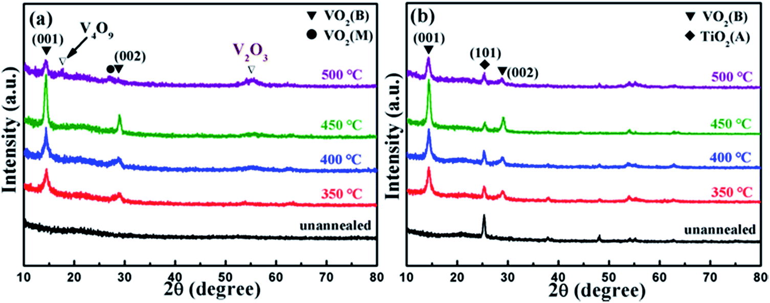 | ||
| Fig. 1 GIXRD patterns of the as-deposited samples: (a) VO2/SiO2 films and (b) VO2/TiO2 films at different annealing temperatures. | ||
Subsequently, the two samples with the best crystallization (the films annealed at 450 °C, the olive line in Fig. 1) were selected for further characterization. Note that the VO2/SiO2 film, in comparison, is deposited directly on the SiO2/Si substrate. According to the discussion above, both samples clearly possess relatively good VO2 crystallinity with a pure B phase structure.
The corresponding Raman spectra are shown in Fig. 2(a). Both the spectra of VO2/TiO2 (the olive line) and VO2/SiO2 (the red line) exhibit Raman bands centered at 193 cm−1, which corresponds to the VO2(B) phase structure.34 The Raman bands centered at 145 cm−1 are derived from the TiO2(A) phase for the VO2/TiO2 film (the olive line) and TiO2 buffer layer (the blue line). The phase structures characterized by Raman spectra coincide with the GIXRD results.
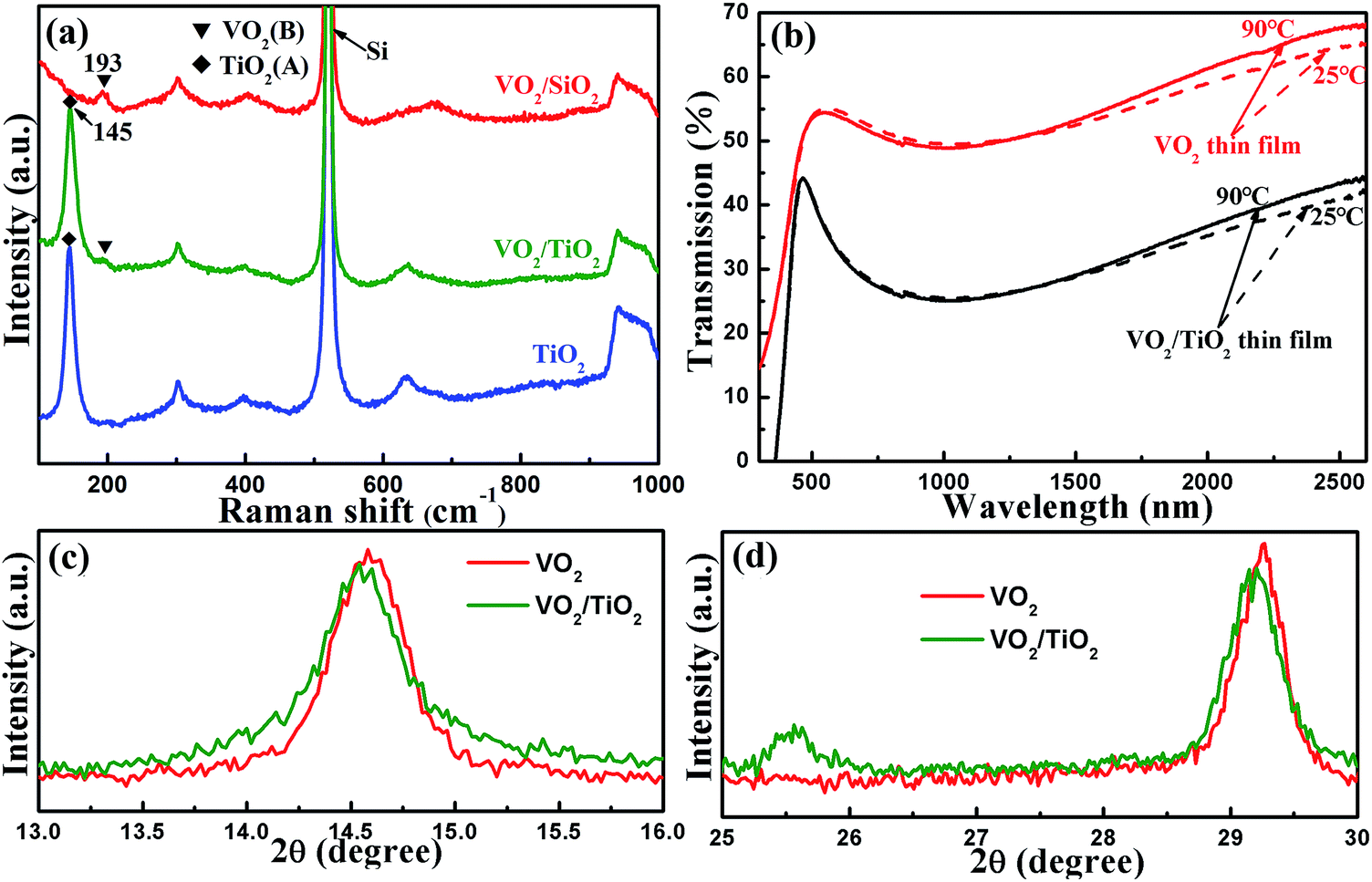 | ||
| Fig. 2 (a) Raman spectra of the as-deposited samples: TiO2 buffer layer, VO2/TiO2 film and VO2/SiO2 film. (b) Transmittance spectra at 25 °C and 90 °C for the as-prepared VO2 film, the VO2/TiO2 film deposited on quartz substrates, and the annealed films. Fine XRD scans from 13° to 16° (c) and 25° to 30° (d), which correspond to the (001) and (002) lattice planes of VO2(B); the scans show slight shifts in the XRD peak positions of both samples. | ||
As mentioned in Section 1, VO2(M) undergoes a semiconductor-to-metal transition (SMT) at ∼67 °C, which is accompanied with a sharp change in optical transmittance in the infrared (IR) range across the phase transition temperature,1,35 while VO2(B) does not experience SMT.12 Therefore, besides XRD and Raman, the transmittance spectra at ∼67 °C can be employed to determine the existence of VO2(M) in the VO2/TiO2 and VO2/SiO2 films. The as-deposited films grown on quartz substrates were inserted into the UV-vis spectrophotometer to measure the optical transmission spectra in the wavelength range from 300 nm to 2600 nm at 25 °C and 90 °C, and the results are plotted in Fig. 2(b). For the sake of convenience, the transmittances at 90 °C and 25 °C and the difference in the transmittances of two types of films at λ = 2500 nm are listed in Table 1. For the VO2 (the two red curves) and the VO2/TiO2 (the two black curves) samples, the transmittance exhibits slight variations (within 3%) before and after the SMT in the IR range, which further confirms the presence of VO2(B) phase structures and the absence of VO2(M) in the VO2/TiO2 and VO2/SiO2 samples.
| Sample | T2500 nm (25 °C) (Tr) | T2500 nm (%) (90 °C) | ΔT2500 nm (%) |
|---|---|---|---|
| VO2 film | 68.1 | 65.1 | 3.0 |
| VO2/TiO2 film | 44.3 | 42.0 | 2.3 |
In particular, fine XRD scans are presented in Fig. 2(c) and (d). Slight shifts of the (001) and (002) diffraction peaks to lower angles (shifts of approximately 0.03° and 0.06°, respectively) are observed in the VO2(B)/TiO2(A) film compared with the VO2(B)/SiO2 film, which indicates a wider distance between (001) and (002) lattice planes in the VO2(B) induced by TiO2(A).
3.2. Structure and morphology of VO2(B)/TiO2(A) film
To investigate the effect of the TiO2 buffer layer on the morphology of the VO2 film, we carried out TEM characterizations for both above-mentioned samples. The cross-section TEM image in Fig. 3(a) shows that a uniform VO2 film with a thickness of 58 nm was grown on the SiO2/Si substrate. Fig. 3(b) shows that a VO2 film with a thickness of ∼67 nm was grown on the TiO2 buffer layer of ∼28 nm. The high-resolution TEM (HRTEM) images of the VO2(B)/SiO2 and VO2(B)/TiO2(A) samples are shown in Fig. 3(c) and (d). It is clearly shown that the distances of the (001) lattice plane are 6.32 Å and 6.50 Å for the VO2(B) films grown on SiO2 and TiO2, respectively. The distance of the (001) lattice plane of VO2(B) in the VO2(B)/TiO2(A) sample is larger than that in VO2(B)/SiO2, which is consistent with XRD results in Fig. 2. Note that the value of the lattice distance was measured from the average of a region in HRTEM images.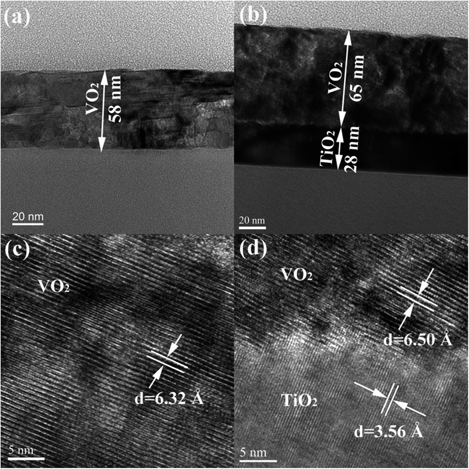 | ||
| Fig. 3 Cross-section TEM images of (a) the as-prepared VO2/SiO2 film and (b) the as-prepared VO2/TiO2 film. HRTEM images of (c) the VO2/SiO2 film and (d) the interface between the VO2 film and the TiO2 buffer layer. | ||
In the VO2(B)/SiO2 sample, the SiO2 substrate is amorphous; therefore, it exerts little strain on the VO2(B) film. On the contrary, the TiO2(A) buffer layer presents a highly (101)-oriented texture, as confirmed in the XRD results in Fig. 2(c) and (d); therefore, the lattice mismatch between the TiO2(A) and VO2(B) may cause a strain on the VO2(B) film. Compared with the distance of the (001) lattice plane, it can be estimated that a tensile strain of approximately 2.85% develops along the c-axis of the VO2(B) film, which is grown on the TiO2(A) substrate.
To analyze the composition of the elements and valence states, XPS measurements were carried out, and the corresponding results are shown in Fig. 4. V 2p and O 1s photoelectron spectra are presented in Fig. 4(a) and (b) for the surface region of the VO2(B)/SiO2 and VO2(B)/TiO2(A) samples, respectively. Owing to spin–orbit splitting, the V 2p spectra demonstrate a typical two-peak pattern for V (2p3/2 and 2p1/2). The Lorentzian–Gaussian sum function was used to divide the V 2p and O 1s peaks and to evaluate the chemical state and stoichiometry of the films. For the V 2p3/2 peaks, there are two peaks centered at approximately 515.41/515.54 eV and 516.79/516.90 eV, which can be assigned to the oxidation states of V4+ and V5+, respectively (515.41 eV for V4+ and 516.79 eV for V5+). The V5+ oxidation state is present because the samples are oxidized after exposure to atmosphere. The peaks centered at 522.93 eV and 523.18 eV are assigned to the V 2p1/2 core level. The O 1s photoelectron spectra are also divided into two peaks because there is more than one chemical state. The peaks centered at 529.27 eV and 529.44 eV refer to the low-binding-energy components (LEEC) and are assigned to the O 1s core peak of O2− binding to V ions. Moreover, the peaks centered at 531.65 eV and 531.75 eV are presumably directly related to the oxygen vacancies.36 For both samples, the V4+ and V5+ valences are evaluated and the content of V4+ valence is much higher than the latter (the fraction percentages of two samples are estimated as 96.39% and 91.59%, respectively), which indicates that vanadium dioxide is the main phase although a small amount of oxygen-rich states with V5+ valence exist.
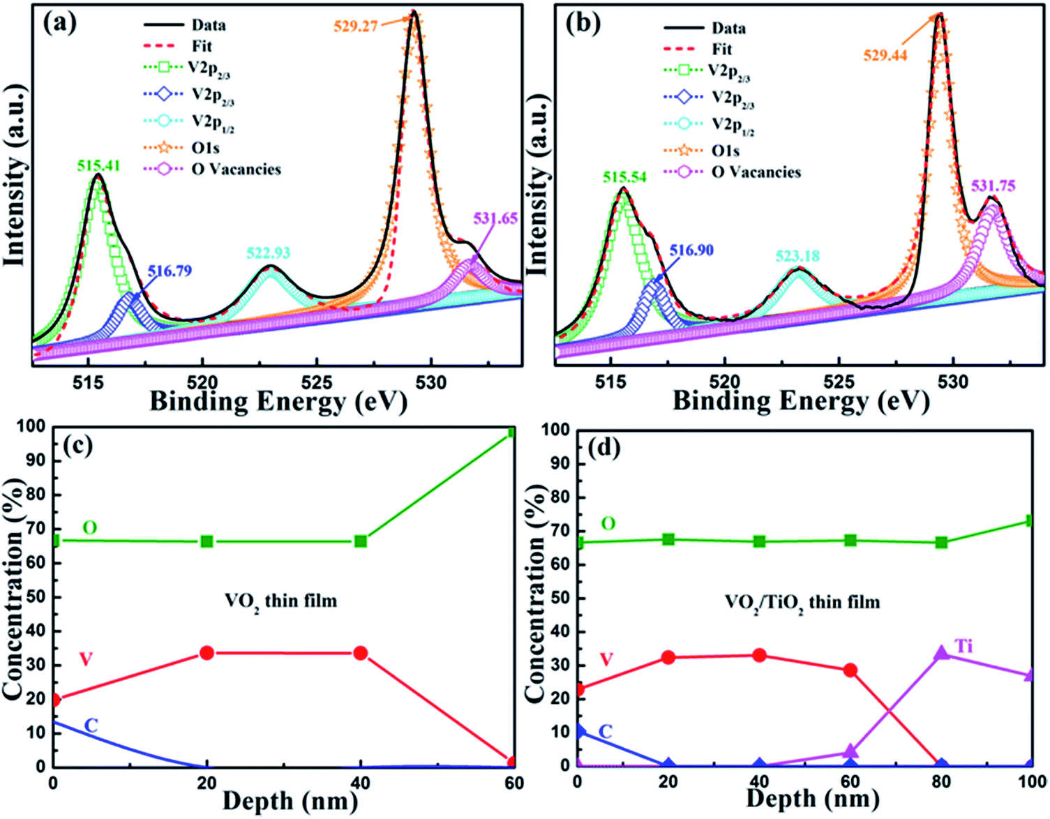 | ||
| Fig. 4 V 2p and O 1s photoelectron spectra for (a) the as-prepared VO2/SiO2 film, and (b) the as-prepared and annealed VO2/TiO2 film. XPS depth profiles of (c) the as-prepared VO2/SiO2 film, and (d) the as-prepared and annealed VO2/TiO2 film. | ||
Fig. 4(c) and (d) show the compositional depth profiles of the VO2(B)/SiO2 and the VO2(B)/TiO2(A) samples determined by XPS. The results demonstrate that C, V, and O co-exist in both samples. The existence of C on the surface of samples can be attributed to adventitious carbon-based contaminants, and the binding energy for the C 1s peak at 284.60 eV is used as the reference for calibration. Fig. 4(c) and (d) show that the O/V ratio near the surface is relatively greater than the O/V ratio inside the films. Other than the influence of the C element on the surface and the diffusion of the atoms from the substrate/buffer layer, the concentration of the primary V and O elements in both samples is relatively stable, and the O/V ratio of is approximately 1.97 and 2.02–2.08 for the VO2(B)/SiO2 and the VO2(B)/TiO2(A) samples, respectively, which further indicates that the films are mainly composed of pure VO2. In addition, the thickness of the VO2(B)/SiO2 and VO2(B)/TiO2(A) films determined by the XPS depth profiles are less than 60 nm and 80 nm, respectively, which is consistent with the TEM measurements.
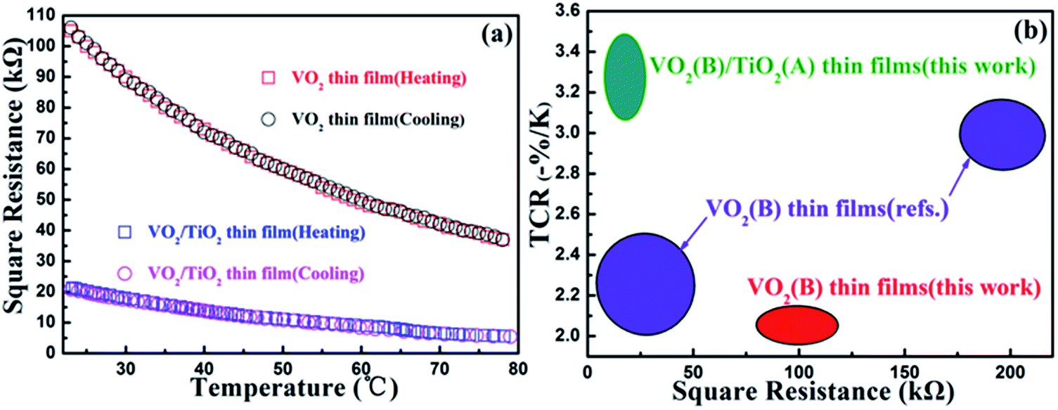 | ||
| Fig. 5 Resistance–temperature curves of (a) the as-prepared VO2(B)/SiO2 thin film, and the as-prepared and annealed VO2(B)/TiO2 thin film. (b) Temperature coefficient of resistivity (TCR) and square resistances of the VO2(B)/TiO2 and VO2(B) thin films at 28 °C compared to already reported values (ref. 37 and 38). | ||
3.3. Improved electronic properties of VO2(B)
The temperature-dependent resistivity curves for the VO2(B)/TiO2(A) and VO2(B)/SiO2 films are shown in Fig. 5(a), and the corresponding TCR values and square resistances at room temperature (28 °C) are listed in Table 2. From Fig. 5(a), it can be clearly observed that the cooling branch coincides very well with the heating branch when the resistances of the thin films decrease exponentially as the temperature increases. In addition, the absence of thermal hysteresis is observed in both samples, which also provides strong support for the B phase structure of both films. As expected, compared to the VO2(B)/SiO2 thin film, the VO2(B)/TiO2 thin film with superior electrical properties simultaneously achieves a high TCR (−3.48% K−1) for maximum sensitivity and low square resistance (18.97 kΩ) to minimize thermal noise and Joule heating at 28 °C. The electrical properties (the TCR and the square resistance at 28 °C) of the VO2(B)/TiO2 thin film are also compared with other reported results (Fig. 5(b)). The VO2(B)/TiO2 thin film exhibits a relatively high TCR between −3.06% K−1 and −3.48% K−1 and a low square resistivity between 30.0 kΩ and 10.0 kΩ. These two parameters are superior to values obtained from our VO2(B) thin films and those reported in literature.37,38| Sample | Resistance (kΩ) | TCR (K−1) |
|---|---|---|
| VO2(B) films | 94.00 | −2.13% |
| VO2(B)/TiO2 films | 18.97 | −3.48% |
The high TCR (−3.48% K−1) and low square-resistance of VO2(B) (18.97 kΩ) are closely related to its atomic and electronic structures. Therefore, first-principles calculations, which are advantageous for capturing the complex interplay between the lattice strain, energetic states and electronic properties of a VO2(B) film, may help illuminate the effect of these properties.39–41 Fig. 6(a) presents the crystalline structure of the bulk VO2(B) phase, which exhibits a monoclinic structure (space group C12/m1). From an atomic perspective, VO2(B) can be described as two identical atomic layers that are stacked along the [010] direction. In each atomic layer, the VO6 octahedra are linked by corners to form edge-sharing structures along the [001] direction, and the second layer is shifted by (0.5 0.5 0) relative to the first layer.22,42 Table 3 presents the lattice parameters (a, b, c and β) and band gap (Eg) of VO2(B), and the experimental data are obtained from the ref. 22 and 42 while the calculated data are from our first-principles calculations. A comparison between them shows that the computed lattice parameters are 1.13% larger, 0.97% larger and 0.39% smaller for a, b and c, respectively, compared with the reported data in the references. Moreover, the calculated band gap (Eg) is 0.60 eV, which is also in vicinity of the experimental band gap of 0.65 eV. The comparison between the reported data and our calculation results suggests that the first-principles calculations we conducted are reliable, and they can be employed in subsequent computations of the electronic properties of VO2(B).
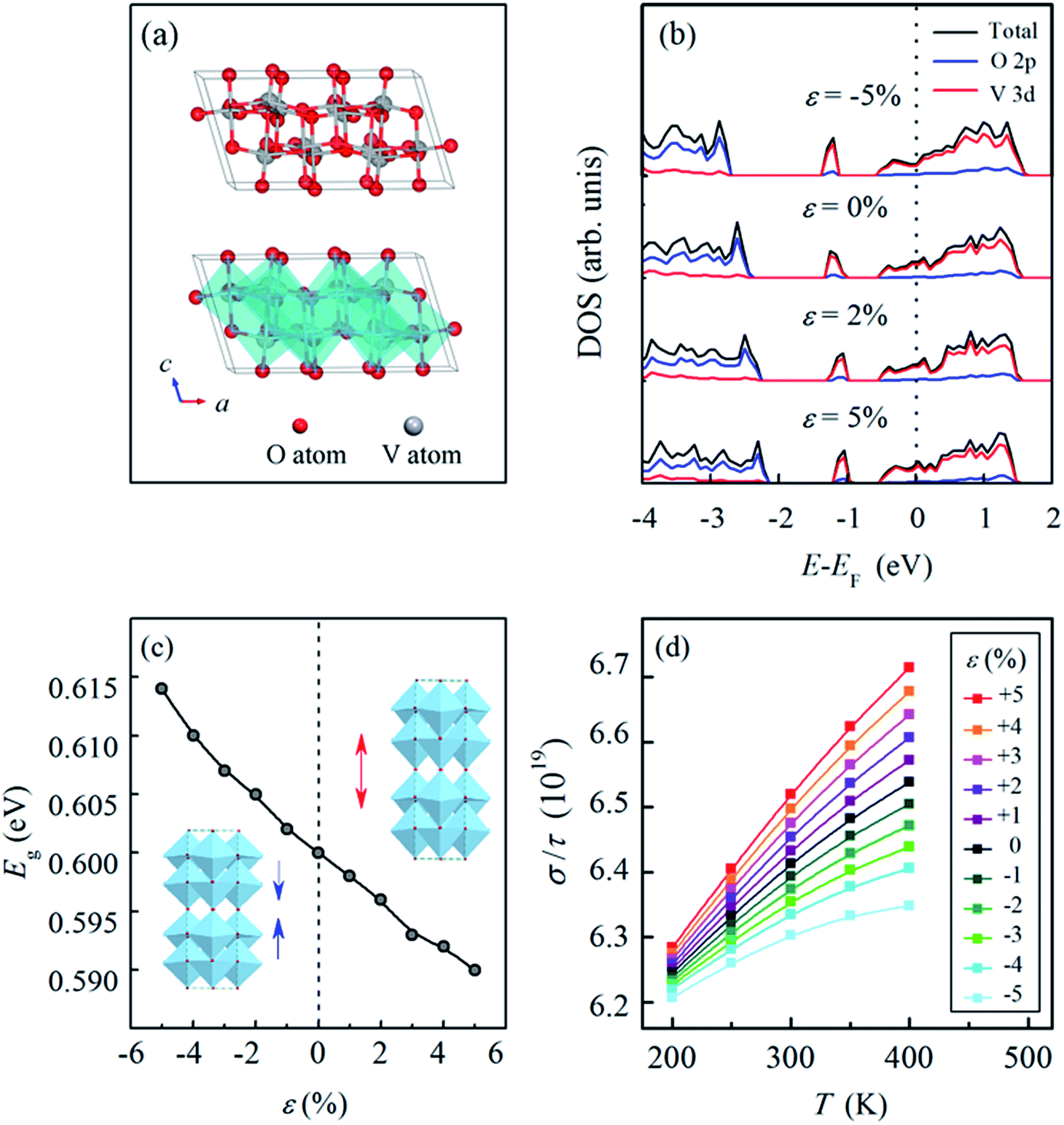 | ||
| Fig. 6 The crystalline structure and arrangement of VO6 octahedra in VO2(B), where the V atoms and O atoms are represented by the gray and red balls, respectively (a). The density of states (DOS) of VO2(B) under different strains along the c-axis, the zero point of the energy axis corresponds to the Fermi level (EF) (b). The variation of the band gap (Eg) as a function of strain along the c-axis in VO2(B) (c). The ratio between the conductivity and relaxation time (σ/τ) of VO2(B) as a function of temperature under the strains ranging from −5% to 5% along the c-axis, σ/τ is given in 1019 (d). | ||
| a (Å) | b (Å) | c (Å) | β (°) | Eg (eV) | Unit cell-internal parameters | ||
|---|---|---|---|---|---|---|---|
| Experiments | 12.093 | 3.702 | 6.433 | 106.970 | 0.65 | V1 (4i): 0.301 0.000 0.721 V2 (4i): 0.400 0.000 0.315 O1 (4i): 0.360 0.000 0.001 O2 (4i): 0.234 0.000 0.344 O3 (4i): 0.443 0.000 0.650 O4 (4i): 0.121 0.000 0.693 | Ref. 22 and 42 |
| Calculations | 12.230 | 3.738 | 6.408 | 109.520 | 0.60 | V1 (4i): 0.298 0.000 0.730 V2 (4i): 0.410 0.000 0.343 O1 (4i): 0.355 0.000 0.005 O2 (4i): 0.234 0.000 0.342 O3 (4i): 0.436 0.000 0.657 O4 (4i): 0.125 0.000 0.677 | This work |
Fig. 6(b) presents the density of states (DOS) of VO2(B) under different strains along the c-axis; this shows that the Fermi energy (EF) is located in the conduction band, which demonstrates the semiconductor characteristic of VO2(B) under strains ranging from −5% to 5% along the c-axis. The highest occupied valence band primarily stems from the V-3d orbital accompanied by a contribution from the O-2p orbital. Fig. 6(c) illustrates the variation in the band gap (Eg) as a function of the strain in VO2(B). It is clearly observed that the band gap (Eg) is widened under compression and narrowed under tension, which indicates that decreasing energy is required for the transition of electrons from occupied states to unoccupied states, i.e., an improvement in the electrical conductivity is realized through tensile strain along the c-axis, which agrees well with our experimental results.
The improvement in the electrical conductivity of VO2(B) under tensile strain can be attributed to two aspects: on one hand, the semiconductor characteristic of VO2(B) is closely correlated with the supercell lengths along the [001] direction, which indicate the distance between adjacent V atoms along the c-axis, i.e., applying a tensile strain along the [001] direction prolongs the distance between adjacent V atoms. Therefore, the tensile strain contributes to less overlapping of V-3d orbitals, which decreases the width of the d band, makes the VO2(B) semiconductor more metallic, and therefore results in an increase in the electrical conductivity. On the other hand, tensile strain along the [001] direction would inject more holes into the VO2(B) samples and thus increase the carrier concentration in VO2(B). This point is confirmed by the areas below the Fermi level in Fig. 6(b). The increased carrier concentrations results in an improvement in the electronic conductivity of VO2(B) under tensile strains.
The temperature coefficient of resistance (TCR) is another major factor for VO2(B). Here the BoltzTrap program,43 which is based on a smoothed Fourier interpolation of the bands, is employed to calculate the semi-classic transport coefficients. The ratio between the conductivity (σ) and the relaxation time (τ) was calculated within a 14 × 16 × 14 k-point mesh in the VO2(B) supercells under different strains along the c-axis. Although the value of σ/τ is not equivalent to the TCR, it can reflect the trend in the variation of conductivity with temperature, which provides important information on the effect of strain.
Fig. 6(d) presents the ratio between the conductivity and relaxation time (σ/τ) of VO2(B) as a function of temperature under the strains from −5% to 5% along the c-axis. It is observed that for all the curves, the ratio increases with increasing temperature for the VO2(B) models under different strains, indicating that VO2(B) experiences an increase in electrical conductance (a decrease in electrical resistance) when the temperature increases, which is in accordance with the negative TCR of VO2(B). In addition, under tensile strains, the curves all show larger slopes than those for samples under compressive strains, and the larger the tensile strain applied to VO2(B) is, the more obvious the increase in the conductivity. Accordingly, our first principles-calculations imply that an improvement in the TCR can be achieved through the application of tensile strain along the c-axis, which corroborates the experimental results illustrated in Fig. 5.
The variation of TCR originates from the combined effects of temperature and strain. As confirmed in our experiments and first-principles calculations, an increase in temperature leads to the presence of more charge carriers, and thus the conductivity of VO2(B) increases with the increase in temperature while the resistivity decreases. Moreover, our first-principles calculations (Fig. 6) indicate that tensile strain along the [001] direction increases the carrier concentration, while compressive strain decreases the carrier concentration. It can be summarized that both increased temperature and tensile strength are constructive factors for the number of charge carriers, whereas an increased temperature and a compressive strength offset each other with respect to the number of charge carriers. Therefore, with the increasing temperature, the more obvious increase in the conductivity can be observed under tensile strain compared to that under compressive strain. In other words, the conductivity of VO2(B) is more sensitive to the change in temperature when VO2(B) is subjected to tensile strain than when it is under compressive strain.
4. Conclusions
In summary, VO2(B) thin films with high TCR (−3.48% K−1) and appropriate square resistance (18.97 kΩ) were successfully achieved by the application of tensile strain (approximately 2.85%) with a TiO2(A) buffer layer. The superior thermal-sensitive properties of the as-prepared thin film make it a very promising material for uncooled IR detector applications since it not only surmounts the shortcomings of VO2(M) and VOx films but also overcomes the weakness exhibited by intrinsic VO2(B) films. The structure and formation mechanism were studied in detail by first-principles calculations. In general, the superior properties of the VO2(B) thin films are attributed to the following: (i) the reduced overlapping of V-3d orbitals due to the tensile strain, which decreases the d band width and makes the semiconductor VO2(B) more metallic, and (ii) the increased carrier concentration in VO2 as a result of tensile strain along the c-axis, both of which contribute to the enhancement of the conductivity and enable the achievement of large TCR values. This study presents a novel facile route for the fabrication and design of high-performance VO2(B) thin films with high TCRs and enhanced conductivity by scaling the lattice strain along the c-axis with suitable buffer layers or substrates.Acknowledgements
The authors gratefully acknowledge the support from the jointed foundation from National Natural Science Foundation of China and the big science facility of Chinese Academy of Sciences (No. U1632108), the National Natural Science Foundation of China (No. 51402182), the Ministry of Science and Technology of China (No. 2016YFB0303901-05), the Science and Technology Commission of Shanghai Municipality (No. 15XD1501700). Gao acknowledges the funding of State Outstanding Young Scholars (51325203) and Changjiang Scholars program.References
- F. Morin, Phys. Rev. Lett., 1959, 3, 34–36 CrossRef CAS.
- T. Yamin, S. Wissberg, H. Cohen, G. Cohen-Taguri and A. Sharoni, ACS Appl. Mater. Interfaces, 2016, 8, 14863–14870 Search PubMed.
- H. Ding, S. S. Dwaraknath, L. Garten, P. Ndione, D. Ginley and K. A. Persson, ACS Appl. Mater. Interfaces, 2016, 8, 13086–13093 CAS.
- J. M. Longo and P. Kierkegaard, Acta Chem. Scand., 1970, 24, 420–426 CrossRef CAS.
- G. Andersson, Acta Chem. Scand., 1956, 10, 623–628 CrossRef CAS.
- Y. Oka, T. Yao and N. Yamamoto, J. Solid State Chem., 1990, 86, 116–124 CrossRef CAS.
- F. Theobald, J. Bernards and R. Cabala, J. Solid State Chem., 1976, 17, 431–438 CrossRef CAS.
- L. Liu, F. Cao, T. Yao, Y. Xu, M. Zhou, B. Y. Qu, B. Pan, C. C. Wu, S. Q. Wei and Y. Xie, New J. Chem., 2012, 36, 619–625 RSC.
- C. Wu, F. Feng, J. Feng, J. Dai, J. Yang and Y. Xie, J. Phys. Chem. C, 2011, 115, 791–799 CAS.
- M. Gurvitch, S. Luryi, A. Polyakov and A. Shabalov, J. Appl. Phys., 2009, 106(104504), 1–15 Search PubMed.
- N. Fieldhouse, S. M. Pursel, R. Carey, M. W. Horn and S. S. N. Bharadwaja, J. Vac. Sci. Technol., A, 2009, 27, 951–955 CAS.
- C. Leroux, G. Nihoul and G. Van Tendeloo, Phys. Rev. B, 1998, 57, 5111–5121 CrossRef CAS.
- S. A. Corr, M. Grossman, Y. Shi, K. R. Heier, G. D. Stucky and R. Seshadri, J. Mater. Chem., 2009, 19, 4362–4367 RSC.
- A. Chen, Z. Bi, W. Zhang, J. Jian, Q. Jia and H. Wang, Appl. Phys. Lett., 2014, 104(071909), 1–4 Search PubMed.
- A. Srivastava, H. Rotella, S. Saha, B. Pal, G. Kalon, S. Mathew, M. Motapothula, M. Dykas, P. Yang, E. Okunishi, D. D. Sarma and T. Venkatesan, APL Mater., 2015, 3(026101), 1–7 Search PubMed.
- D. Y. Wan, P. Xiong, L. L. Chen, S. Q. Shi, I. Ahmad, H. J. Luo and Y. F. Gao, Appl. Surf. Sci., 2017, 397, 30–39 CrossRef CAS.
- H. W. Liu, D. Y. Wan, I. Ahmad, L. L. Chen, B. B. Guo, S. Q. Shi, H. J. Luo and Y. F. Gao, ACS Appl. Mater. Interfaces, 2016, 8, 7884–7890 CAS.
- Y. Zhang, C. Liu, J. Liu, J. Xiong, J. Liu, K. Zhang, Y. Liu, M. Peng, A. Yu, A. Zhang, Y. Zhang, Z. Wang, J. Zhai and Z. L. Wang, ACS Appl. Mater. Interfaces, 2016, 8, 1381–1387 CAS.
- M. W. Zhu, H. L. Wang, H. Lei, Y. J. Zhang, N. Jia and Z. J. Wang, Appl. Phys. A: Solids Surf., 2016, 122(364), 1–7 CAS.
- D. Yao, L. Shi, S. Zhou, H. Liu, Y. Wang, J. Zhao and Y. Li, J. Phys. D: Appl. Phys., 2016, 49, 125301–125307 CrossRef.
- H. Li, X. Wang and J. Liu, Appl. Phys. Lett., 2016, 108(102101), 1–5 Search PubMed.
- Y. Oka, T. Yao, N. Yamamoto, Y. Ueda and A. Hayashi, J. Solid State Chem., 1993, 105, 271–278 CrossRef CAS.
- D. A. H. Hanaor and C. C. Sorrell, J. Mater. Sci., 2011, 46, 855–874 CrossRef CAS.
- G. Kresse and J. Hafner, Phys. Rev. B, 1993, 47, 558–561 CrossRef CAS.
- G. Kresse and J. Furthmuller, Phys. Rev. B, 1996, 54, 11169–11186 CrossRef CAS.
- P. E. Blochl, Phys. Rev. B, 1994, 50, 17953–17979 CrossRef.
- J. P. Perdew, K. Burke and M. Ernzerhof, Phys. Rev. Lett., 1996, 77, 3865–3868 CrossRef CAS PubMed.
- R. M. Wentzcovitch, W. W. Schulz and P. B. Allen, Phys. Rev. Lett., 1994, 72, 3389–3392 CrossRef CAS PubMed.
- T. M. Rice, H. Launois, J. P. Pouget, R. M. Wentzcovitch, W. W. Schulz and P. B. Allen, Phys. Rev. Lett., 1994, 73, 3042–3043 CrossRef CAS PubMed.
- T. J. Huffman, P. Xu, M. M. Qazilbash, E. J. Walter, H. Krakauer, J. Wei, D. H. Cobden, H. A. Bechtel, M. C. Martin, G. L. Carr and D. N. Basov, Phys. Rev. B, 2013, 87(115121), 1–7 Search PubMed.
- S. Kim, K. Kim, C. Kang and B. I. Min, Phys. Rev. B, 2013, 87(195106), 1–5 Search PubMed.
- Y. Cui, S. Shi, L. Chen, H. Luo and Y. Gao, Phys. Chem. Chem. Phys., 2015, 17, 20998–21004 RSC.
- J. Zhang, H. He, Y. Xie and B. Pan, J. Chem. Phys., 2013, 138(114705), 1–7 Search PubMed.
- X. J. Wang, H. D. Li, Y. J. Fei, X. Wang, Y. Y. Xiong, Y. X. Nie and K. A. Feng, Appl. Surf. Sci., 2001, 177, 8–14 CrossRef CAS.
- M. Li, D. B. Li, J. Pan, H. Wu, L. Zhong, Q. Wang and G. H. Li, J. Phys. Chem. C, 2014, 118, 16279–16283 CAS.
- M. P. Lu, C. W. Chen and M. Y. Lu, Phys. Rev. Appl., 2016, 6, 054018 CrossRef.
- H. C. Wang, X. J. Yi and S. H. Chen, Infrared Phys. Technol., 2006, 47, 273–277 CAS.
- H. Wada, M. Nagashima, N. Oda, T. Sasaki, A. Kawahara, M. Kanzaki, Y. Tsuruta, T. Mori, S. Matsumoto, T. Shima, M. Hijikawa, N. Tsukamoto and H. Gotoh, Proc. SPIE, 1998, 3379, 90–100 CrossRef CAS.
- T. Yao, X. Zhang, Z. Sun, S. Liu, Y. Huang, Y. Xie, C. Wu, X. Yuan, W. Zhang, Z. Wu, G. Pan, F. Hu, L. Wu, Q. Liu and S. Wei, Phys. Rev. Lett., 2010, 105(226405), 1–4 Search PubMed.
- J. O. Island, A. Kuc, E. H. Diependaal, R. Bratschitsch, H. S. J. van der Zant, T. Heine and A. Castellanos-Gomez, Nanoscale, 2016, 8, 2589–2593 RSC.
- P. Xiao, X. Fan, L. Liu and W. Lau, Phys. Chem. Chem. Phys., 2014, 16, 24466–24472 RSC.
- S. Zhang, B. Shang, J. Yang, W. Yan, S. Wei and Y. Xie, Phys. Chem. Chem. Phys., 2011, 13, 15873–15881 RSC.
- G. Madsen and D. Singh, Comput. Phys. Commun., 2006, 175, 67–71 CrossRef CAS.
Footnote |
| † These authors contributed equally to this work. |
| This journal is © The Royal Society of Chemistry 2017 |