
 Open Access Article
 This Open Access Article is licensed under a
 Creative Commons Attribution 3.0 Unported Licence
The synthesis of hybrid nanostructure comprising star-shaped GaN nanowires and Si nanoworms
Ji-Hyeon Park†
ab,
Uddipta Chatterjee†a,
San Kanga,
Dae-Young Uma and
Cheul-Ro Lee *a
*a
aSemiconductor Materials Process Laboratory, School of Advanced Materials Engineering, Engineering College, Research Center for Advanced Materials Development (RCAMD), Chonbuk National University, Baekje-daero 567, Jeonju 54896, Republic of Korea. E-mail: crlee7@jbnu.ac.kr
bCenter for Quantum Devices, Department of Electrical Engineering and Computer Science, Northwestern University, Evanston, IL 60208-0893, USA
First published on 3rd May 2017
Abstract
Herein, we proposed a novel hybrid nanostructure comprising unique star-shaped GaN nanowires with Si nanoworms having drifting Au nanoparticles inside. Both nanostructures were simultaneously grown using a MOCVD chamber. Intentional stain was induced while growing the star-shaped GaN nanowires to achieve this new nanostructure. A planned experimental environment was deliberated to facilitate the simultaneous growth of the Si nanoworms along with the star-shaped GaN nanowires. After the growth process, various characterization techniques were applied to study the crystallinity and structural and optical properties of the hybrid structure. The growth mechanisms for both structures were also systematically investigated. It was found that a high concentration of the n-dopant source drives the growth of the star-shaped GaN nanowires by suppressing the lateral growth at the high dopant-concentrated vertices of the conventional hexagonal-shaped GaN nanowires. On the other hand, a surplus amount of the same dopant source assists the Si nanoworms to grow. Si nanoworms follow the base-growth mechanism, in which after a while, the Au nanoparticles start to drift inside the Si nanoworms. Finally, the photocurrent of the hybrid structure was measured and compared with that of the star-shaped GaN nanowires only. It is concluded from the photocurrent measurements that the grown hybrid structure is a better candidate for future optoelectronic devices.
1. Introduction
Recently, oriented one-dimensional (1-D) nanostructures, such as nanowires (NWs) and nanorods, have attracted significant research interest due to their potential application as building blocks in many opto-electronic devices, such as photovoltaics,1–4 light-emitting diodes (LEDs),5–8 field effect transistors (FETs),9–12 nanolasers,13–15 and electric generators.16,17 Moreover, the carrier diffusion coefficient and electron recombination time of the ordered 1D nanostructure were found to be larger than those for polycrystalline films, which in turn remarkably increased the diffusion length of the minority carrier.18–20 It has been reported in studies that the electron transport in crystalline nanowires is several orders of magnitude faster than that in the polycrystalline material, which may remarkably reduce the recombination loss and enhance the photocurrent.21 Additionally, nanowires (NWs), due to their high surface-to-volume ratio compared to that of their bulk material, show a significant reduction in the defect and dislocation densities. However, despite these prolific advantages, the nanostructured devices made of these homogeneous material arrangements often suffer from low efficiency and poor performance. Thus, many researchers have studied nanostructured devices fabricated with a heterogeneous material assembly. The III-nitrides family, with attractive properties such as a direct energy band gap, high thermal stability, and high electron mobility, comprises one of the most investigated materials paired with the most common semiconductor material silicon (Si).22–26 Y. B. Tang et al. investigated a photovoltaic device containing p-GaN nanowires grown on a n-Si substrate and reported a relatively high Jsc value around 7.6 mA cm−2.27 A demonstration of a III-nitride/Si tandem solar cell was reported by L. Reichertz et al. in 2009.28 K. M. A. Saron et al. fabricated another hybrid photovoltaic device comprising GaN and n-Si.29 Although these tandem structures are very interesting to study, the high cost and complexity of the fabrication techniques often hinder their further development. In this background, we studied unique star-shaped GaN NWs, which may offer a greater surface to volume ratio than the conventional hexagonal-shaped materials along with simultaneously grown Si nanoworms bearing Au nanoparticles inside.Herein, we report the growth and characterization of novel star-shaped GaN NWs along with Si nanoworms bearing Au nanoparticles. Both the nanostructures were simultaneously grown to achieve a hybrid structure by designing a favorable experimental environment. In addition, extensive characterization methods were used to study the structural and optical properties of the grown hybrid structure, comprising the star-shaped GaN NWs and Si nanoworms with Au nanoparticles inside. The respective growth mechanisms were also systemically investigated and reported.
2. Experimental procedure
All the samples studied in this report were grown on a Si (111) substrate using a home-designed horizontal MOCVD system. Trimethylgallium (TMGa) and ammonia (NH3) were used as the gallium (Ga) and nitrogen (N2) sources, respectively. For the n-type doping, silane (SiH4) was used as the source. Hydrogen (H2) was supplied as the carrier gas. All the chemicals were used without any further purification. Before the deposition, the Si (111) substrate was cleaned in an ultrasonic bath with organic solvents including acetone (CH3COCH4) and methanol (CH3OH). The same substrate was then subjected to solutions containing DI water![[thin space (1/6-em)]](https://www.rsc.org/images/entities/char_2009.gif) :H2O2:H2SO4 (1:1:3) and H2O:HF (50:1) to etch out any inorganic impurities and the native oxide layer. The etching time for both the solutions was 5 minutes. Lastly, the substrate was dried under a flow of N2.
:H2O2:H2SO4 (1:1:3) and H2O:HF (50:1) to etch out any inorganic impurities and the native oxide layer. The etching time for both the solutions was 5 minutes. Lastly, the substrate was dried under a flow of N2.
After the cleaning steps, the Si substrate was subjected to a DC magneto sputtering system for 10 s to deposit the Au nanoparticles. Then, at 720 °C, 12 pairs of GaN seed layers were prepared using a MOCVD system operating in the pulse growth mode. TMGa and NH3 were used as the precursors for Ga and N, respectively. The TMGa flow rate was kept constant at 0.3 sccm throughout the process, whereas the NH3 flow rate was 3 SLM. For the carrier gas, H2 was supplied at the rate of 1 SLM. During the pulse mode, each precursor was sequentially flowed for 3 min.
In the next step, for the growth of the star-shaped GaN nanowires (NWs) and Si nanoworms, the temperature was initially increased to 800 °C. Then, the temperature was kept constant throughout the process. We followed a conventional MOCVD growth process this time. Therefore, all the precursors were supplied together. The Ga source TMGa was supplied at the rate of 0.3 sccm, whereas the NH3 gas flow rate was kept constant at 3 SLM. The carrier gas H2 was continuously supplied at the flow rate of 1.5 SLM. During the growth process, 100 ppm SiH4 gas was utilized for the n-type doping. The flow rate for SiH4 was maintained at 10 sccm and 5 sccm for the simultaneous growth of the star-shaped GaN nanowires (NWs) with Si nanoworms and star-shaped GaN nanowires (NWs) only, respectively. The total growth time was 1 hour. During the entire growth time, the chamber pressure was kept at the constant value of 600 Torr. Finally, the Au:Ni (8:2) metal contacts were formed to measure the photocurrent, employing a DC magneto sputtering system. The entire growth process is schematically presented in Fig. 1.
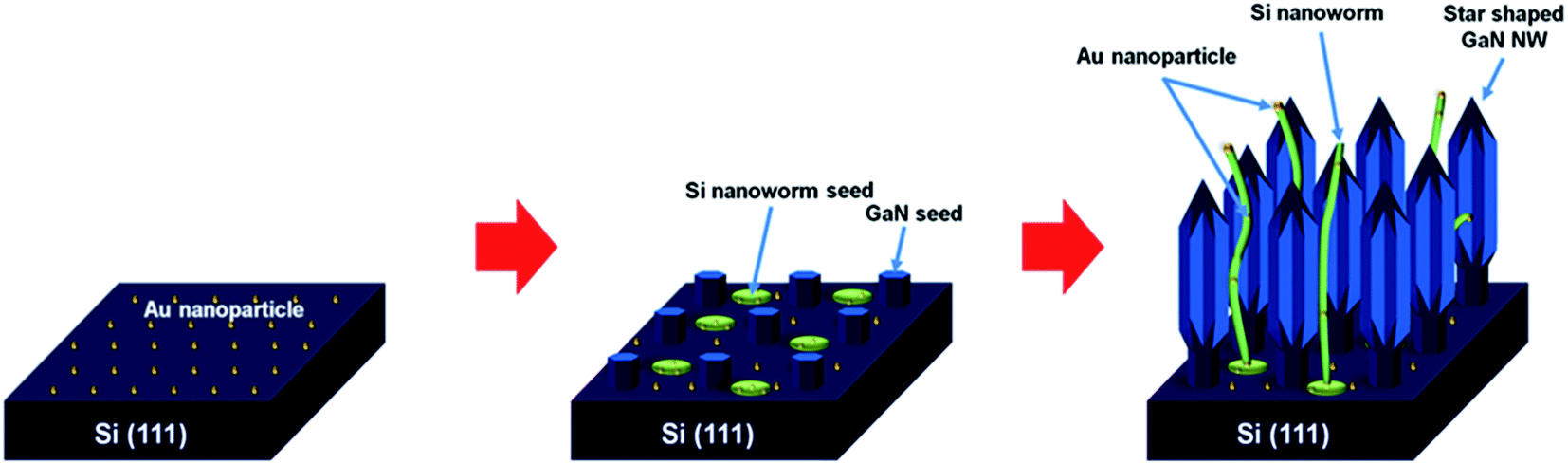 | ||
| Fig. 1 A schematic of the simultaneous growth process for the star-shaped GaN NWs along with Si nanoworms. | ||
The surface morphology of the grown nanowires was characterized by employing a Hitachi S-7400 field effect scanning electron microscope (FE-SEM), operated at 15 kV. X-ray diffraction (XRD) measurements were carried out utilizing a PANalytical EMPYREAN instrument. The crystallinity was examined using a JEM-ARM-200F Cs-corrected-field emission transmission electron microscopy (Cs-corrected-FE-TEM) instrument equipped with an EDX facility at the accelerating voltage of 200 kV. The optical properties were investigated via carrying out photoluminescence (PL) experiments at room temperature. A He–Cd 325 nm laser was used as the photon source. The detector used for photoluminescence investigation was a InGaAs detector. The photocurrent of the fabricated devices was measured by employing a solar simulator (McScience Lab 100) as the light source. This light source generated white light at the maximum power density 100 mW cm−2.
3. Results and discussion
To study the surface morphology and structures of the grown GaN NWs and Si nanoworms, we employed the FE-SEM technique. Fig. 2(a, b, and c) show the obtained FE-SEM images. In Fig. 2(a), only the star-shaped GaN NWs can be seen. Highly dense star-shaped GaN NWs showing growth in the (002) direction or vertical direction can be predominantly observed in Fig. 2(a and b). The top-view of a single NW exposing the 12 facets clearly showing the star shape is shown in the inset of Fig. 2(a). In Fig. 2(b), along with the star-shaped GaN NWs, the Si nanoworms were observed. The Si nanoworms form a highly dense structure similar to a fishing net. The bright spots seen inside the Si nanoworms in Fig. 2(b) are the Au nanoparticles. In Fig. 2(c), a single star-shaped GaN NW is displayed, exposing the sharp edges. The base of the NW was an undoped GaN seed, which was hexagonal in shape. However, the introduction of SiH4 at a high flow rate restrains the lateral growth, which in turn results in the final star-shaped structure. This phenomenon has been discussed later in this study. Furthermore, the crystallinity and optical characterization were carried out using XRD and PL characterization techniques, respectively.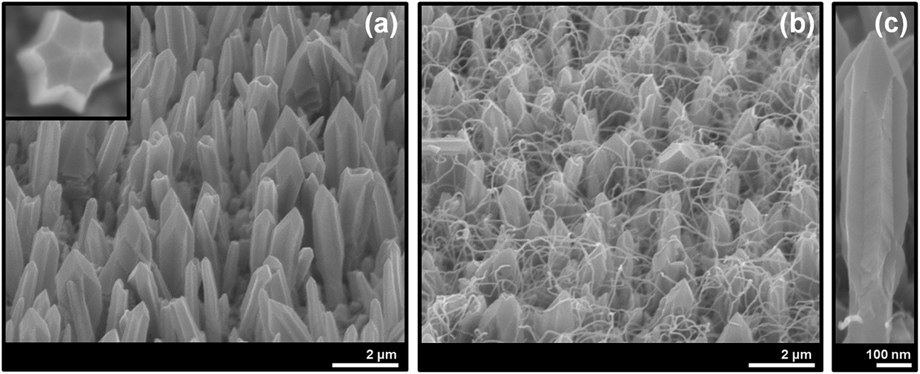 | ||
| Fig. 2 (a) An FE-SEM image showing the star-shaped GaN NWs only. The inset image displays the top-view of a star-shaped GaN NW, (b) an FE-SEM image showing the grown hybrid structure comprising star-shaped GaN NWs and Si nanoworms, and (c) an FE-SEM image showing a single star-shaped GaN NW. | ||
Additionally, XRD measurements were performed on the grown structures to investigate the induced stress. In Fig. 3(a), the obtained XRD patterns for both structures are presented. Clearly, the dominant peak was (002), appearing at 2θ = 34.2°. However, the stress free c-axis directional growth of the GaN NWs shows a peak value of 34.562°.30 This shift in the XRD 2θ value was attributed to the tensile stain in the z-direction, which suppressed the lateral growth of the NWs to retain the final star shape. Similar findings have been reported by B. G. Park et. al.31 The other three minor peaks represent the (100), (101), and (102) semi-polar planes. The XRD diffractograms for both structures are similar in nature. Thus, it can be concluded that the Si nanoworms do not induce any additional stress in the final hybrid structure. The residual strain in the z-direction and in-plane strain were estimated to be 0.0029 and −0.042, respectively, for the star-shaped GaN NWs only.31,32 However, the same stain values for the hybrid nanostructure comprising star-shaped GaN NWs and Si nanoworms were found to be 0.0043 and −0.0054.31,32 This enhancement in compressive strain in the in-plane was attributed to the increased Si doping, which in turn modifies the shape of the synthesized GaN NWs. The PL spectra of both structures are shown in Fig. 3(b). In the spectrum representing the star-shaped GaN NWs only, the peak position at 365.66 nm displays the band edge emission. While a yellow luminescence (YL) at 559.64 nm is associated with the native Ga vacancy defects (VGa) and surface defects.33 However, in the hybrid structure comprising star-shaped GaN NWs and Si nanoworms, the dominant GaN peak position was at the wavelength value of 363.67 nm. This blue shift in the hybrid structure was caused by compressive stress, which confirmed the XRD findings. In the case of the hybrid structure, the YL peak was suppressed, which was due to the excessive doping effect. E. R. Glaser et al. reported the same phenomenon in their report while investigating a GaN system doped with shallow acceptors.34 A longitudinal phonon recombination peak was also observed in the hybrid structure at 401.45 nm.33,34 Next, the crystallinity of the grown structures was examined by Cs-corrected-FE-TEM.
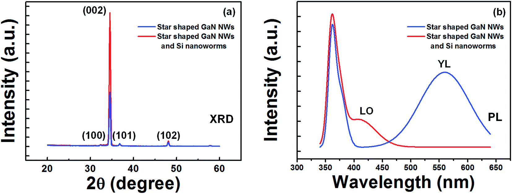 | ||
| Fig. 3 (a) The XRD patterns for both structures showing the dominant c-plane (002) peak position and (b) the PL spectra for both structures showing the dominant band edge emission with YL (for the star-shaped GaN NWs only) and longitudinal phonon recombination (for the hybrid structure). | ||
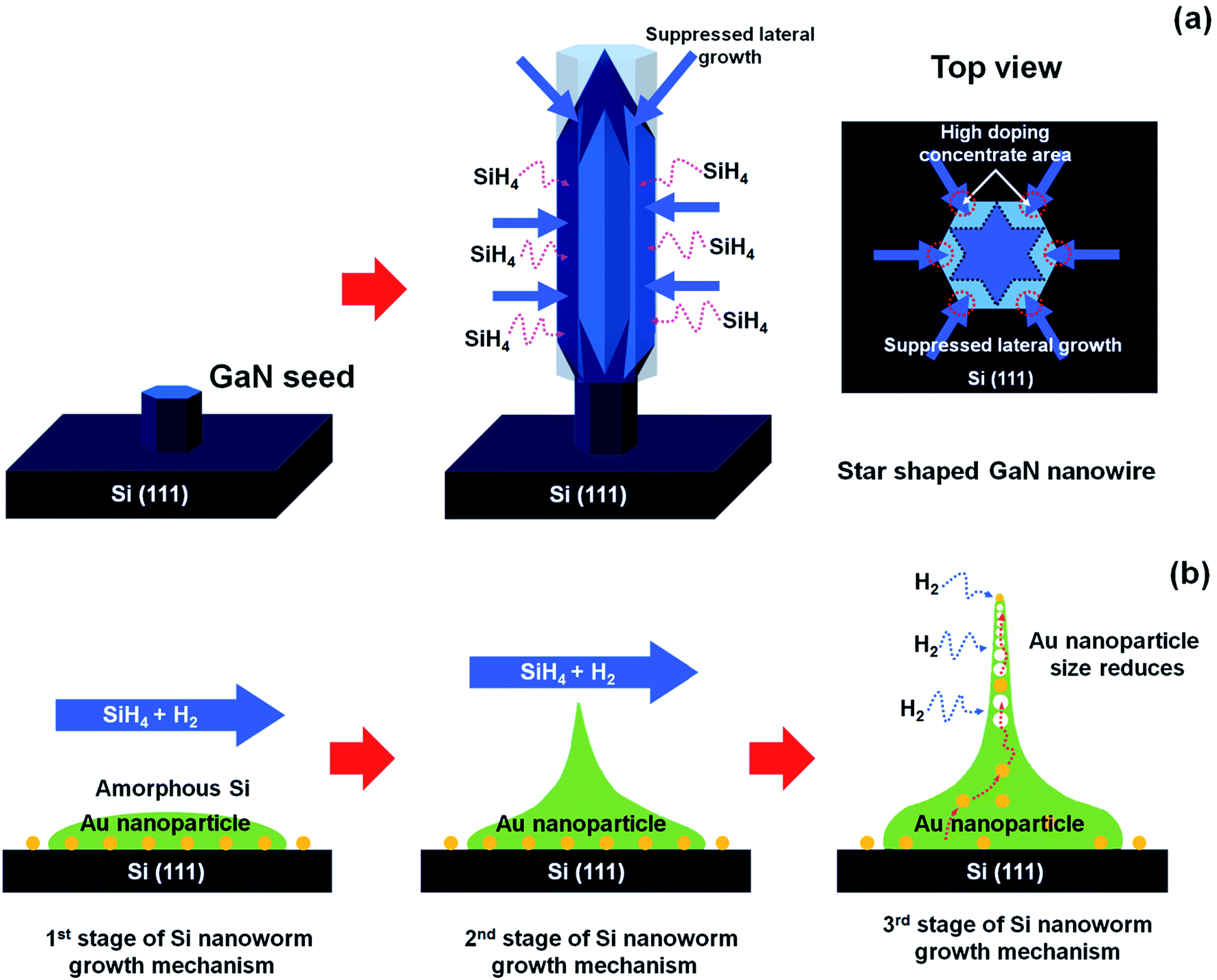
The Cs-corrected-FE-TEM images and EDX mapping data of the grown structures are shown in Fig. 4(a–i). The Cs-corrected-FE-TEM dark field image of a star-shaped GaN NW is displayed. The hexagonal GaN seed can be seen at the bottom of the NW. No threading dislocation defect was detected in the star-shaped GaN NWs. The EDX mapping data for the star-shaped GaN NWs is displayed in Fig. 4(b), presenting all the desired materials. Fig. 4(c and d) represent the inverse fast Fourier transform (IFFT) image and the transferred image of the star-shaped GaN NWs, respectively, revealing the wurtzite structure and well-aligned lattice. To investigate the Si-doping on the surface of the materials, focused ion beam (FIB) milling was performed to expose the cross-section of a single star-shaped GaN NW. The EDX mapping data of the cross-sectional NWs can be seen in Fig. 4(e). Concentrated Si dopants on the NW surface can be clearly perceived in this image. A Cs-corrected-FE-TEM image of a Si nanoworm is displayed in Fig. 4(f), showing the Au nanoparticles inside. Area ① in Fig. 4(f) was designated to have a high magnified Cs-corrected-FE-TEM image, which is shown in Fig. 4(g). Clearly, the Au nanoparticles can be seen inside the bamboo-shaped Si nanoworm. A high-magnification image of the Si nanoworms bearing the Au nanoparticles is presented in Fig. 4(h). The inset image of the same figure reveals the lattice fringes of the Au nanoparticles. EDX mapping data of Fig. 4(i) confirm presence of all the desired materials, i.e. Si and Au, in the Si nanoworms. The unique Si nanoworms containing Au nanoparticles are very interesting in terms of their growth mechanism. In Fig. 5, a plausible growth mechanisms for both the nanostructures are schematically shown. In Fig. 5(a), the growth mechanism of the star-shaped GaN NW's is explained. In the 1st stage of growth, an hexagonal GaN seed was formed along the c-axis growth direction (002). Then, in the 2nd stage of growth, a high concentration SiH4 gas was added to suppress the lateral growth. Fang et al. studied the Si dopant distribution on the GaN NWs facets and found that the distribution was higher on the surface.35 However, as evident from Fig. 4(e), all the vertices of the star-shaped GaN NWs have a higher concentration of the n-type dopant Si, which acts as a shape breaker of the conventional hexagonal GaN NWs structure. Previously, many researchers have reported that Si dopants help towards vertical growth and suppress the lateral growth in the GaN NWs.36–39 Therefore, it can be concluded that the high concentration of Si dopants employed in this current investigation stopped the lateral growth process and broke the conventional hexagonal shape.
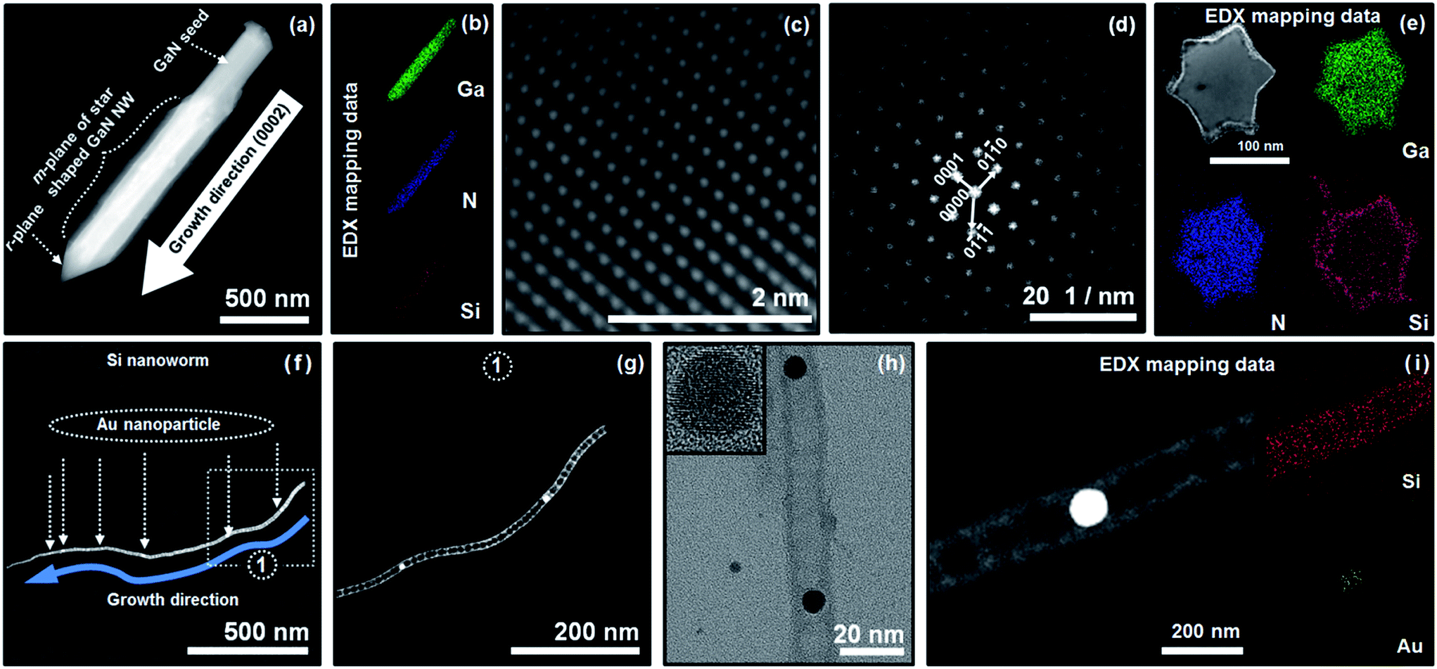 | ||
| Fig. 4 (a) A Cs-corrected-FE-TEM image of a single star-shaped GaN NW showing the hexagonal seed and pyramidal r-plane top. (b) EDX mapping data of a star-shaped GaN NW along the (002) growth direction, showing all the desired elements. (c) An inverse fast Fourier transform (IFFT) image of the star-shaped GaN NWs showing no dislocation defects. (d) The transferred image of the star-shaped GaN NWs revealing the wurtzite structure. (e) EDX mapping data of the star-shaped GaN NWs along the top r-plane direction presenting all the desired elements. (f) A Cs-corrected-FE-TEM image of a single Si nanoworm showing the Au nanoparticles inside. (g) A high magnification Cs-corrected-FE-TEM image of a single Si nanoworm taken at in the designated area (①) shown in the previous figure clearly displaying the bamboo shape inside. (h) A high magnification Cs-corrected-FE-TEM image of a single Si nanoworm clearly showing the Au nanoparticles inside. The inset displays a single Au nanoparticle with lattice fringes. (i) EDX mapping data of a single Si nanoworm, revealing all the desired elements. | ||
 | ||
| Fig. 5 (a) A schematic of the growth mechanism to realize the star-shaped GaN NWs. (b) A schematic of the growth mechanism to realize the Si nanoworms, following a base-growth mechanism. | ||
On the other hand, during the growth of the star-shaped GaN NWs, the excess Si present in the growth chamber (flow rate: 10 sccm) assisted the growth of the Si nanoworms. In the 1st stage of Si nanoworm growth, a large area of an amorphous Si seed layer was formed, covering a number of Au nanoparticles. In this stage, the Au–Si nanoparticles infused together to produce a solid solution. Additionally, the eutectic melting point for the Au–Si solid solution was stated to be 363 °C by A. Sarikov in 2011.40 Therefore, at the temperature to grow the star-shaped GaN NWs i.e. 800 °C, eutectic melting of the solid solution comprising Au–Si occurred during the 2nd stage of growth. Hence, the Si nanoworms started growing in an upward direction, following the base-growth mechanism, whereas the Au nanoparticles remained at the bottom and Si nanoworms started to grow. Y. Yan et al. in their review article described the base-growth mechanism for carbon nanotubes in detail.41 However, in the presence of an excess of H2 and SiH4, the Au nanoparticles began to decompose from the base and due to the pressure difference inside the nanoworm, because of the size variation from base to top, they started to drift upwards. During this instant drifting, the Au nanoparticles expedited inside the hollow shape of the Si nanoworms. K. Yadav et al. have observed and reported a similar phenomenon in 2014.42 This stage is schematically represented as the 3rd stage in Fig. 5(b). However, although the shape of the Au nanoparticles remained spherical, the size of the nanoparticles continuously decreased, depending on the Si nanoworm diameter.
The FE-SEM images obtained during different stages of the Si nanoworm growth without the Ga and N sources are shown in Fig. 6(a–e). The 1st stage of growth or the formation of the Au–Si solid solution as small islands on the Si substrate can be seen in Fig. 6(a). After the eutectic melting, the Si nanoworm growth begins from the island-like seeds, which can be observed in Fig. 6(b). The growth of Si nanoworms following the base-growth mechanism with drifting Au nanoparticles from base to top is represented in Fig. 6(c). The complete structure of the Si nanoworms after 1 hour is displayed in Fig. 6(d), where the drifted Au nanoparticles can be found at the top of the Si nanoworms. Fig. 6(e) reveals different Si nanoworms containing the drifted Au nanoparticles at various locations inside the nanoworm structure. All the FE-SEM images shown in Fig. 6(a–e) are in accordance with the aforementioned growth mechanism.
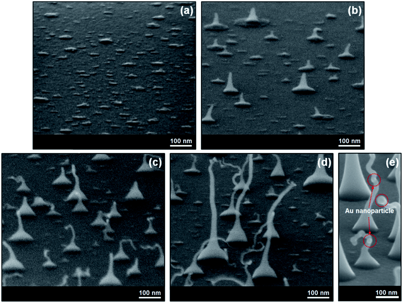 | ||
| Fig. 6 (a) An FE-SEM image of the island-like seed formation of the Au–Si solid solution. (b) An FE-SEM image at the beginning of the Si nanoworms following the base-growth mechanism. (c) An FE-SEM image of the Si nanoworms showing the drifted Au nanoparticles at the top. (d) An FE-SEM image of the final Si nanoworms structure after 1 h of growth. (e) An FE-SEM image of various Si nanoworms with drifted Au nanoparticles. | ||
Furthermore, the opto-electronic applicability of both nanostructures was tested via photocurrent measurements. Fig. 7(a) shows the obtained photocurrent measurement results in comparison with those of the conventional hexagonal-shaped GaN NWs. At the positive bias value of 1.5 V, the star-shaped GaN NWs displayed a photocurrent of 4.04 mA, whereas the photocurrent of the hybrid structure comprising the star-shaped GaN NWs and Si nanoworms bearing Au nanoparticles inside was measured to be up to 7.1 mA. On the other hand, the photocurrent observed for the conventional hexagonal-shaped GaN NWs was measured to be 1.447 mA at 1.5 V, which was previously reported by our group elsewhere.30 This enhancement in the photocurrent can be attributed to the embedded Au nanoparticles, which increase the photosensitivity of the Si nanoworms by generating hot electrons, which in turn enhance the photocurrent of the final hybrid nanostructure. A similar phenomenon has been reported by M.-S. Hu et al.43 The photoresponsivity was estimated by the Iphoto/(illuminated area × power density of light).44,45 The maximum light power density value i.e. 100 mW cm−2 was used in the current investigation. At a bias of 1.5 V, the absolute photoresponsivity of the hybrid structure comprising the star-shaped GaN NWs and Si nanoworms bearing Au nanoparticles inside was calculated to be 71 mA W−1, and the same for the star-shaped GaN NWs only was obtained to be 40.4 mA W−1. The reduced empty spaces between the individual NWs and the larger photoconductive area due to the presence of the Si nanoworms are the noteworthy causes for the enhancement in the photoresponsivity of the hybrid structure. Photoresponsivity analysis further proves that the hybrid structure was superior in terms of the opto-electronic applications when compared to the star-shaped GaN NWs only. The photocurrent of the hybrid structure at various light power densities is shown in Fig. 7(c). In the inset of the same figure, the photocurrent evolution of the star-shaped GaN NWs only with variable light power density is shown. The photocurrent was observed to be enhanced with an increasing incident optical power density, as expected. The photocurrent values at a bias of 1.5 V are plotted against the optical power density and fitted by the simple power law, Iphoto ∞ PX, where P is the incident optical power of the white light source and the exponent X determines the density of trap levels between the Fermi level and the conduction band of the hybrid structure.44,46 These trap levels absorb the photogenerated carrier and significantly reduce the photocurrent. Even at a lower optical power density, the photogenerated carriers should not be absorbed by these trap levels and contribute to the photocurrent. Therefore, upon increasing the optical or light power density, the photocurrent should linearly increase in a defect-free structure. The same plot of the synthesized hybrid structure is shown in Fig. 7(d). The value of the exponent X should be considerably smaller than 1 for a structure containing a higher density of traps. However, when the photocurrent values are fitted in Fig. 7(d), the photocurrent shows X to be approximately 0.87. While the same for the star-shaped GaN NWs only was found to be 0.75 (the inset in Fig. 7(d)). The evidence of the minimal defects or trap states in the synthesized hybrid structure reveals that these MOCVD grown hybrid structure comprising star-shaped GaN NWs and Si nanoworms bearing Au nanoparticles inside can be a prolific alternative for efficient opto-electronic devices.
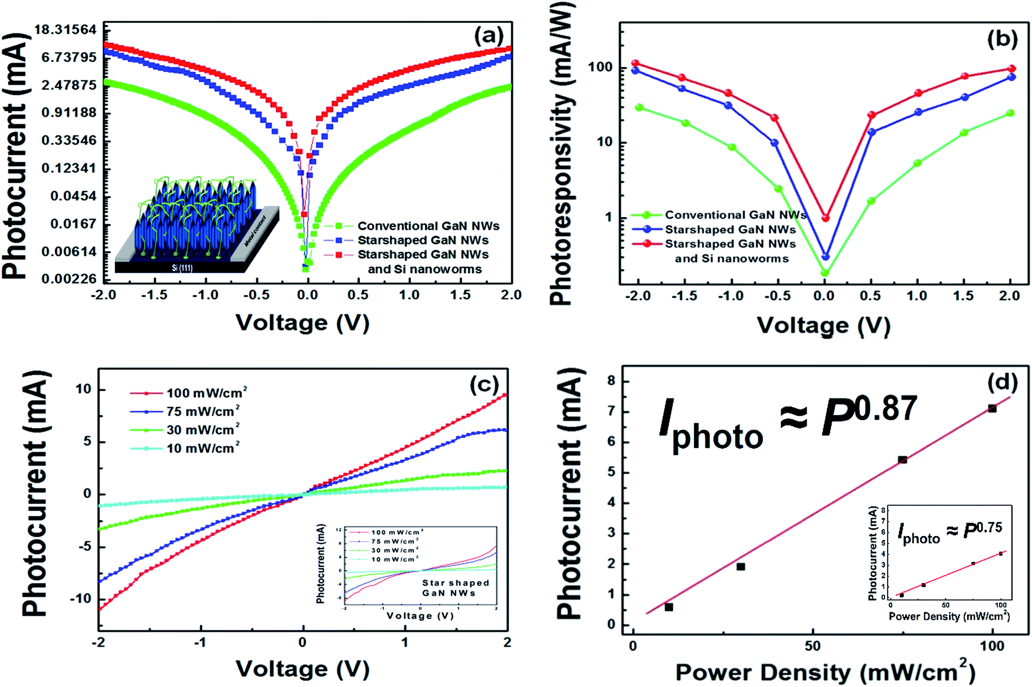 | ||
| Fig. 7 (a) The I–V measurement plot of both the grown nanostructures showing the improved photocurrent of the hybrid structure due to the Si nanoworms with embedded Au nanoparticles along with the conventional hexagonal GaN NWs reported previously.30 (b) The photoresponsivity vs. voltage plot for both the grown nanostructures showing the improved photoresponsivity of the hybrid structure due to the smaller space between the individual NWs and larger photoconductive area due to the presence of the Si nanoworms. (c) The I–V plot of the grown hybrid nanostructure with varying optical power density; the I–V plot of the star-shaped GaN NWs only with varying optical power density is shown in the inset. (d) The linear increase in the photocurrent of the hybrid nanostructure measured at various optical power densities, which was attributed to the reduced density of the trap levels in the photoconductive channel; the exponent X in the power law has a high value of approximately 0.87. This measurement was performed with the bias fixed at 1.5 V. | ||
4. Conclusion
In summary, a unique novel star-shaped GaN NW structure was grown on a Si substrate. Additionally, with the help of an excess n-type dopants (SiH4), Si nanoworms could be simultaneously realized with the star-shaped GaN NWs. Various characterization techniques were employed to study the crystalline and optical properties of both grown novel nanostructures. The Si nanoworms were found to be unique in the sense of their growth mechanism, which was investigated in detail. The Si nanoworms were found to grow according to a base-growth mechanism, whereas the star-shaped GaN NWs were realized by suppressing the lateral growth by the high concentration of SiH4. In other words, intentional strain was induced to design the growth of the star-shaped GaN NWs. Moreover, it was found that the drifted Au nanoparticles assisted the formation of the bamboo shape of the Si nanoworms. Both nanostructures were found to be photoresponsive. The photocurrent for the hybrid structure comprising star-shaped GaN NWs and Si nanoworms with drifted Au nanoparticles was higher than that of the star-shaped GaN NWs only. Therefore, it was concluded that the unique hybrid nanostructure has the potential of mixing III–V materials and Si for the next generation high power-high efficient photoelectronic devices.Conflict of interest
The authors declare no competing financial interest.Acknowledgements
This work was supported by the National Research Foundation of Korea (NRF) grant funded by the Korea government (MSIP) (No. 2015R1A2A2A01002877) and (No. 2015R1A4A1042417).References
- M. F. Cansizoglu, S. M. Hamad, D. P. Norman, F. Keles, E. Badraddin, T. Karabacak and H.-W. Seo, PiN InGaN nanorod solar cells with high short-circuit current, Appl. Phys. Express, 2015, 8, 1–4 CrossRef CAS.
- E. Garnett and P. Yang, Light trapping in silicon nanowire solar cells, Nano Lett., 2010, 10, 1082–1087 CrossRef CAS PubMed.
- J. Kupec, R. L. Stoop and B. Witzigmann, Light absorption and emission in nanowire array solar cells, Opt. Express, 2010, 18, 27589–27605 CrossRef CAS PubMed.
- R. R. Lapierre, A. C. E. Chia, S. J. Gibson, C. M. Haapamaki, J. Boulanger, R. Yee, P. Kuyanov, J. Zhang, N. Tajik, N. Jewell and M. A. Rahman, III–V nanowire photovoltaics: Review of design for high efficiency, Phys. Status Solidi RRL, 2013, 7, 815–830 CrossRef CAS.
- A.-L. Bavencove, D. Salomon, M. Lafossas, B. Martin, A. Dussaigne, F. Levy, B. Andre, P. Ferret, C. Durand, J. Eymery, L. S. Dang and P. Gilet, Light emitting diodes based on GaN core/shell wires grown by MOVPE on n-type Si substrate, Electron. Lett., 2011, 47, 765–766 CrossRef CAS.
- X. Dai, A. Messanvi, H. Zhang, C. Durand, J. Eymery, C. Bougerol, F. H. Julien and M. Tchernycheva, Flexible Light-Emitting Diodes Based on Vertical Nitride Nanowires, Nano Lett., 2015, 15, 6958–6964 CrossRef PubMed.
- S. M. Sadaf, Y. H. Ra, T. Szkopek and Z. Mi, Monolithically Integrated Metal/Semiconductor Tunnel Junction Nanowire Light-Emitting Diodes, Nano Lett., 2016, 16, 1076–1080 CrossRef CAS PubMed.
- V. Neplokh, A. Messanvi, H. Zhang, F. H. Julien, A. Babichev, J. Eymery, C. Durand and M. Tchernycheva, Substrate-Free InGaN/GaN Nanowire Light-Emitting Diodes, Nanoscale Res. Lett., 2015, 10, 447–452 CrossRef PubMed.
- S. Han, W. Jin, D. Zhang, T. Tang, C. Li, X. Liu, Z. Liu, B. Lei and C. Zhou, Photoconduction studies on GaN nanowire transistors under UV and polarized UV illumination, Chem. Phys. Lett., 2004, 389, 176–180 CrossRef CAS.
- D. Saccheto, M. H. Ben-Jamaa, G. De Micheli and Y. Leblebici, Fabrication and characterization of vertically stacked Gate-All-Around Si nanowire FET arrays, ESSDERC 2009-Proc 39th Eur Solid-State Device Res Conf, 2009, pp. 245–248 Search PubMed.
- S. N. Cha, J. E. Jang, Y. Choi, G. A. J. Amaratunga, G. W. Ho, M. E. Welland, D. G. Hasko, D.-J. Kang and J. M. Kim, High performance ZnO nanowire field effect transistor using self-aligned nanogap gate electrodes, Appl. Phys. Lett., 2006, 89, 1–4 CrossRef.
- O. Knopfmacher, A. Tarasov, W. Fu, M. Wipf, B. Niesen, M. Calame and C. Schonenberger, Nernst limit in dual-gated Si-nanowire FET sensors, Nano Lett., 2010, 10, 2268–2274 CrossRef CAS PubMed.
- Q. Li, J. B. Wright, W. W. Chow, T. S. Luk, I. Brener, L. F. Lester and G. T. Wang, Single-mode GaN nanowire lasers, Opt. Express, 2012, 20, 17873–17879 CrossRef CAS PubMed.
- J. C. Johnson, H.-J. Choi, K. P. Knutsen, R. D. Schaller, P. Yang and R. J. Saykally, Single gallium nitride nanowire lasers, Nat. Mater., 2002, 1, 106–110 CrossRef CAS PubMed.
- H. Zhou, M. Wissinger, J. Fallert, R. Hauschild, F. Stelzl, C. Klingshirn and H. Kalt, Ordered, uniform-sized ZnO nanolaser arrays, Appl. Phys. Lett., 2007, 91, 2005–2008 Search PubMed.
- Y. Qin, X. Wang and Z. L. Wang, Microfibre-nanowire hybrid structure for energy scavenging, Nature, 2008, 451, 809–813 CrossRef CAS PubMed.
- W. Wang, F. Jia, Q. Huang and J. Zhang, A new type of low power thermoelectric micro-generator fabricated by nanowire array thermoelectric material, Microelectron. Eng., 2005, 77, 223–229 CrossRef CAS.
- G. Mor, K. Shankar, M. Paulose, O. K. Varghese and C. A. Grimes, Use of Highly-Ordered TiO2 Nanotube Arrays in Dye-Sensitized Solar Cells, Nano Lett., 2006, 6, 215–218 CrossRef CAS PubMed.
- B. Kannan, K. Castelino and A. Majumdar, Design of Nanostructured Heterojunction Polymer Photovoltaic Devices, Nano Lett., 2003, 3, 1729–1733 CrossRef CAS.
- K. M. Coakley and M. D. McGehee, Conjugated polymer photovoltaic cells, Chem. Mater., 2004, 16, 4533–4542 CrossRef CAS.
- K. Zhu, N. R. Neale, A. Miedaner and A. J. Frank, Enhanced Charge-Collection Efficiencies and Light Scattering in Dye-Sensitized Solar Cells Using Oriented TiO2 Nanotubes Arrays, Nano Lett., 2007, 7, 69–74 CrossRef CAS PubMed.
- R. Calarco, InN nanowires: Growth and optoelectronic properties, Materials, 2012, 5, 2137–2150 CrossRef CAS.
- A. D. L. Bugallo, L. Rigutti, G. Jacopin, F. H. Julien, C. Durand, X. J. Chen, D. Saloman, J. Eymery and M. Tchernycheva, Single-wire photodetectors based on InGaN/GaN radial quantum wells in GaN wires grown by catalyst-free metal–organic vapor phase epitaxy, Appl. Phys. Lett., 2011, 98, 1–3 CrossRef.
- G. Meneghesso, G. Verzellesi, F. Danesin, F. Rampazzo, F. Zanon, A. Tazzoli, M. Meneghini and E. Zanoni, Reliability of GaN high-electron-mobility transistors: State of the art and perspectives, IEEE Trans. Device Mater. Reliab., 2008, 8, 332–343 CrossRef CAS.
- L. J.-H. Lin and Y.-P. Chiou, Optical design of GaN/InxGa1−xN/cSi tandem solar cells with triangular diffraction grating, Opt. Express, 2015, 23, A614–A624 CrossRef CAS PubMed.
- H. P. T. Nguyen, Y. L. Chang, I. Shih and Z. Mi, InN p-i-n nanowire solar cells on Si, IEEE J. Sel. Top. Quantum Electron., 2011, 17, 1062–1069 CrossRef CAS.
- Y. B. Tang, Z. H. Chen, H. S. Song, C. S. Lee, H. T. Cong, H. M. Cheng, W. J. Zhang, I. Bello and S. T. Lee, Vertically aligned p-type single-crystalline GaN nanorod arrays on n-type Si for heterojunction photovoltaic cells, Nano Lett., 2008, 8, 4191–4195 CrossRef CAS PubMed.
- L. a. Reichertz, I. Gherasoiu, K. M. Yu, V. M. Kao, W. Walukiewicz and J. W. Ager, Demonstration of a III-Nitride/Silicon Tandem Solar Cell, Appl. Phys. Express, 2009, 2, 1–3 Search PubMed.
- K. M. A. Saron and M. R. Hashim, Broad visible emission from GaN nanowires grown on n-Si (1 1 1) substrate by PVD for solar cell application, Superlattices Microstruct., 2013, 56, 55–63 CrossRef CAS.
- D.-Y. Um, A. Mandal, D.-S. Lee, J.-H. Park and C.-R. Lee, Demonstration of n-GaN: Si NWs having ultrahigh density and aspect ratio via a 3-step growth method using MOCVD, CrystEngComm, 2016, 18, 480–487 RSC.
- B.-G. Park, R. S. Kumar, S.-T. Lee, M.-D. Kim, J.-E. Oh, S.-G. Kim and T.-G. Kim, A Study on Strain and Shape of GaN Nanorods with Variation of Si Concentration Grown on Patterned Si(111) Substrates, J. Nanosci. Nanotechnol., 2016, 16, 11486–11489 CrossRef CAS.
- L. Zhang, K. Cheng, S. Degroote, M. Leys, M. Germain and G. Borghs, Strain effects in GaN epilayers grown on different substrates by metal organic vapor phase epitaxy, J. Appl. Phys., 2010, 108, 1–6 CrossRef PubMed.
- M. A. Reshchikov and H. Morko, Luminescence properties of defects in GaN, J. Appl. Phys., 2005, 97, 1–95 CrossRef.
- E. R. Glaser, J. A. Freitas, B. V. Shanabrook, D. D. Koleske, S. K. Lee, S. S. Park and J. Y. Han, Optically detected magnetic resonance of (effective-mass) shallow acceptors in Si-doped GaN homoepitaxial layers, Phys. Rev. B: Condens. Matter Mater. Phys., 2003, 68, 1–6 CrossRef.
- Z. Fang, E. Robin, E. Rozas-Jiménez, A. Cros, F. Donatini, N. Mollard, J. Pernot and B. Daudin, Si Donor Incorporation in GaN Nanowires, Nano Lett., 2015, 15, 6794–6801 CrossRef CAS PubMed.
- R. Koester, J. S. Hwang, C. Durand, D. L. S. Dang and J. Eymery, Self-assembled growth of catalyst-free GaN wires by metal–organic vapour phase epitaxy, Nanotechnology, 2010, 21, 015602 CrossRef CAS PubMed.
- X. J. Chen, B. Gayral, D. Sam-Giao, C. Bougerol, C. Durand and J. Eymery, Catalyst-free growth of high-optical quality GaN nanowires by metal–organic vapor phase epitaxy, Appl. Phys. Lett., 2011, 99, 1–3 Search PubMed.
- C. Tessarek, M. Heilmann, E. Butzen, A. Haab, H. Hardtdegen, C. Dieker, E. Spiecker and S. Christiansen, The role of si during the growth of gan micro- and nanorods, Cryst. Growth Des., 2014, 14, 1486–1492 CAS.
- R. Koester, J. S. Hwang, D. Salomon, X. Chen, C. Bougerol, J. P. Barnes, D. L. S. Dang, L. Rigutti, A. D. L. Bugallo, G. Jacopin, M. Tchernycheva, C. Durand and J. Eymery, M-plane core-shell InGaN/GaN multiple-quantum-wells on GaN wires for electroluminescent devices, Nano Lett., 2011, 11, 4839–4845 CrossRef CAS PubMed.
- A. Sarikov, Metal induced crystallization mechanism of the metal catalyzed growth of silicon wire-like crystals, Appl. Phys. Lett., 2011, 99, 97–100 CrossRef.
- Y. Yan, J. Miao, Z. Yang, F.-X. Xiao, H. B. Yang, B. Liu and Y. Yang, Carbon nanotube catalysts: recent advances in synthesis, characterization and applications, Chem. Soc. Rev., 2015, 44, 3295–3346 RSC.
- K. Yadav, B. R. Mehta and J. P. Singh, Template-free synthesis of vertically aligned crystalline indium oxide nanotube arrays by pulsed argon flow in a tube-in-tube chemical vapor deposition system, J. Mater. Chem. C, 2014, 2, 6362–6369 RSC.
- M. S. Hu, H. L. Chen, C. H. Shen, L. S. Hong, B. R. Huang, K. H. Chen and L.-C. Chen, Photosensitive gold-nanoparticle-embedded dielectric nanowires, Nat. Mater., 2006, 5, 102–106 CrossRef CAS PubMed.
- R. Yan, D. Gargas and P. Yang, Nanowire photonics, Nat. Photonics, 2009, 3, 569–576 CrossRef CAS.
- H. Lee, K. Heo, J. Park, Y. Park, S. Noh, K. S. Kim, C. Lee, B. H. Hong, J. Jian and S. Hong, Graphene-nanowire hybrid structures for high-performance photoconductive devices, J. Mater. Chem., 2012, 22, 8372–8376 RSC.
- J. S. Jie, W. J. Zhang, Y. Jiang, X. M. Meng, Y. Q. Li and S. T. Lee, Photoconductive characteristics of single-crystal CdS nanoribbons, Nano Lett., 2006, 6, 1887–1892 CrossRef CAS PubMed.
Footnote |
| † Equal Contribution. |
| This journal is © The Royal Society of Chemistry 2017 |