
 Open Access Article
 This Open Access Article is licensed under a Creative Commons Attribution-Non Commercial 3.0 Unported Licence
Metal-seed planting fabrication of W–W18O49 core shell nanoflowers for gas sensors†
Jianyi Luo *,
Yudong Li,
Xiwei Mo,
Youxin Xu and
Qingguang Zeng
*,
Yudong Li,
Xiwei Mo,
Youxin Xu and
Qingguang Zeng
Laboratory of Optoelectronic Materials and Devices, School of Applied Physics and Materials, Wuyi University, Jiangmen, Guangdong 529020, P. R. China. E-mail: luojiany@mail3.sysu.edu.cn
First published on 8th June 2017
Abstract
In this study, a new kind of metal oxide nanoflower has been controllably synthesized on pre-designed regions of a substrate by a metal-seed planting method, in which the nanoflowers only appear where the metal seeds are planted. The material characterization technologies have proved that such nanoflowers are composed of a nanowire shell and a nanoparticle core, and their structures can be assigned to monoclinic W18O49 and cubic W phases, respectively. The growth mechanism of the W–W18O49 core shell nanoflowers has also been investigated by recording the growth process from the metal-seed W particles to the nanoflowers in the metal planting method. Furthermore, after annealing in air, the W–W18O49 nanoflowers were completely oxidized into WO3 nanoflowers, the hydrogen gas sensor based on a Pt coated WO3 (Pt–WO3) nanoflower film was fabricated, and the gas sensing test showed that it is a potential material to resolve the unstable sensing performance of normal metal oxide sensors at room temperature.
1. Introduction
Hydrogen has received wide spread attention as a clean and renewable alternative to carbon-based fuels; in particular, it has recently become an important fuel for new-energy-power vehicles.1–3 Therefore, the safe utilization and storage of hydrogen in the fuel producer/supplier environment and the end-user environment has become a critical aspect for meeting the growing hydrogen demand.4–6 The U.S. department of energy published a list of target specifications for hydrogen safety sensors as early as the year 2007,7 including the operating temperature in the range of −30 °C to 80 °C, and the detection range of 0.1% to 10% in ambient air. However, no existing technology can meet all of these target specifications. For the typical example, although metal oxide (MOX) sensors are widely used for hydrogen safety, due to their small sizes and facility of mass production, this kind of sensor needs to operate at high temperature (approximately 300 °C or greater) to obtain stable and measurable conductivities,8,9 which poses the imminent danger of explosion when hydrogen leaks occur. Recently, metal oxide nanostructures have been demonstrated to have excellent hydrogen gas-sensing performances at room temperature.10–12Tungsten oxide has been widely investigated as a new functional material, due to its crucial applications in chromic devices, gas sensors, photo-catalysts, super-capacitors and field emission devices.13–19 WO3 nanostructure films, coated by noble metals such as Pt or Pd as catalysts, have shown high sensitivity to H2 in air at room temperature, and good repeatability.20–23 Particularly, the Pt, Pd or their oxide particle-coated WO3 films composed of one-dimensional nanostructures (such as nanowires, nanorods, nanoneedles, nanofibers and nanotubes) have been proved to have a more outstanding performance in hydrogen detection in previous reports by our group24,25 and other groups.26–32 However, there is a long way to go before this new kind of nanomaterial is used in the actual sensor devices. One of the critical challenges is to controllably synthesize these nanostructures in the pre-designed regions (like the region between two electrodes) in the electronic unit devices, and keep these nanostructures fixed and stable on the substrate.
In this study, we develop a new fabrication method for the tungsten oxide nanostructures, in which tungsten particles are planted as metal-seeds on the pre-designed regions of the substrate, and the tungsten oxide nanoflowers only grow where the metal-seeds are planted during thermal oxidation. This new method is hereafter referred to as the metal-seed planting method. Tungsten oxide nanoflowers are controllably synthesized on the pre-designed regions by this method, and their material structures are studied by scanning electron microscopy (SEM), X-ray diffraction (XRD) spectroscopy and scanning transmission electron microscopy (STEM) technologies. The growth mechanisms of such nanoflower structures are also investigated by recording the process from the metal-seed W particles growing into the nanoflowers in the metal-seed planting method. The hydrogen sensors based on the Pt–WO3 nanoflowers film (obtained by annealing tungsten oxide nanoflowers film and then coating with Pt nanoparticles) as a sensing unit are also fabricated in this study; a layer composed of tungsten oxide nanowires was inserted between the nanoflowers and the substrate in order to increase the contact area and improve the adhesive force between the nanoflowers and the substrate. The gas sensing test demonstrated that our sensor based WO3 nanoflowers would be expected to overcome the unstable sensing performance at room temperature in the normal MOX sensors.
2. Experimental
2.1 Metal-seed planting method for W–W18O49 nanoflowers
The experimental setup consisted of a vacuum chamber (Φ 300 mm × 400 mm), two copper electrodes, a rotary pump system, and a gas controlling system. A tungsten boat (15 mm × 3 mm × 0.3 mm) was placed and fixed on the copper electrodes.The W–W18O49 nanoflowers were synthesized in two steps: (1) tungsten particles as metal-seeds were planted on the substrates; (2) the seeds were oxidized into metal oxide nanostructures by a thermal oxidation. In the thermal oxidation, the quartz substrates were placed above the boat. When the vacuum chamber was first evacuated to about 5 Pa, mixed gases of high purity argon and oxygen (both 99.99% pure) were introduced into the chamber. The flow rate of argon was fixed at 200 sccm, while the flow rate of oxygen was 2.0 sccm. The tungsten boat was then heated to 900 °C and held at the peak temperature for a period of time denoted in this study as the heat-retention time (i.e., 5, 10, and 15 min). Finally, the sample underwent natural cooling to room temperature (25 °C) in a vacuum.
2.2 Thermal evaporation method for the tungsten oxide nanowire layer in the sensor device
The experimental setup was the same as for the method of synthesizing W–W18O49 nanoflowers. Before thermal oxidation, high purity tungsten powder (0.5 g, 99.95%) was spread out on the bottom of the tungsten boat. Quartz substrates were covered on the bottom of a tungsten boat and a gap between the substrates and the boat was used as the nanowire growth region. First of all, when the vacuum chamber was evacuated down to about 5 Pa, mixed gases of high purity argon gas and oxygen gas (both were 99.99% pure) were introduced into the chamber. The flow rates of argon gas and oxygen gas were fixed at 100 sccm and 0.5 sccm respectively. Then, the tungsten boat was heated to 800 °C and maintained at this temperature for 5 min in a vacuum. Finally the sample underwent natural cooling to room temperature (25 °C), under vacuum.2.3 Annealing in air for the sensor devices
Both tungsten oxide nanowires and W–W18O49 nanoflowers were oxidized to the monoclinic WO3 phase by annealing the samples in air at 500 °C for more than 3 hours.2.4 Magnetron sputtering method for the Pt nanoparticle catalyst and Pt electrodes in the sensor device
A thin layer of Pt nanoparticles as a catalyst was deposited onto the surfaces of WO3 nanoflowers by magnetron sputtering, in which a high-purity platinum target and argon gas (99.99%) were used. The amount of the Pt catalyst is an important parameter affecting the WO3 nanoflower film, and it was determined by just controlling the sputtering current and sputtering time. The optimal sputtering current and sputtering time were 5 mA and 20 s, respectively.Two Pt electrodes (3 mm × 3 mm) were prepared on both sides of the nanoflower film by using a baffle mask with a spacing of about 5.0 mm in the above magnetron sputtering. The optimal sputtering current and sputtering time were 20 mA and 20 s, respectively.
2.5 Characterization
The morphologies, chemical compositions, and structures of the prepared products were characterized by field SEM (Nova Nano SEM 432), TEM (FEI Tecnai GZ F30 at 300 kV) equipped with an energy-dispersive X-ray spectroscopy (EDS) detector and X-ray diffraction spectroscopy by using an X-ray source of Cu Kα radiation (XRD, X'pert Pro).2.6 Gas sensing properties test
In order to detect the voltage or resistance change of a hydrogen sensor induced by the different concentrations of hydrogen gas, a hydrogen sensor testing system was expediently realized as shown in Fig. 1(a). This testing system was composed of a detection circuit, a computer, an airtight chamber, a controllable temperature board (to keep the temperature constant at a certain temperature), and a small fan (enabling the uniform distribution of hydrogen in the airtight chamber). The hydrogen flow was introduced into the chamber from a hydrogen generator, and the concentration of hydrogen gas ρ was determined by
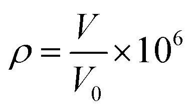 | (1) |
 | ||
| Fig. 1 Illustrations for (a) the hydrogen sensor testing system and (b) the detection circuit in the hydrogen sensor testing system. | ||
During the detection, a hydrogen sensor was reacted with the hydrogen gas, and its resistance was changed. This change in the resistance was converted into voltage change by the voltmeter (Victor 86E), and then the data for the voltage change was immediately input into the computer. The valve of the airtight chamber was closed when the capability testing of the sensor was started. First, a certain volume of pure hydrogen gas (the concentration determined by eqn (1), falling within the range of 50–5000 ppm) was introduced into the chamber for a period of time and the resistance of the hydrogen obviously decreased. Then, when the chamber was opened in air, external air entered the chamber and the resistance of the hydrogen sensor gradually recovered, due to the reduction of the concentration of hydrogen gas in the chamber.
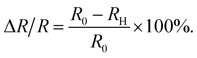
The detection circuit is shown in Fig. 1(b), in which the gas sensor is connected with a resistor of 10 MΩ to avoid a short circuit load. A voltmeter was used to monitor the voltage change across the hydrogen sensor, and its internal resistance was determined by disconnecting the sensor R0 in the circuit of Fig. 1(b); the voltage value indicated in the voltmeter just equaled to half of the source voltage, meaning its internal resistance was also 10 MΩ. The resistance of the series resistor and the internal resistance of the voltmeter were denoted by RL and RV, respectively. U is the voltage of the voltage-stabilized source (here it equaled to 23 V). U0, and UH represent the voltages across the sensor before (at t = 0 minute) and after exposure to hydrogen gas, respectively. R0 and RH represent the resistance of the sensor before (at t = 0 minutes) and after exposure to hydrogen gas. ΔR/R is the resistance change rate of the gas sensor. The resistance change rate can be derived from the detection circuit as shown in Fig. 1(b). R0, RH, and ΔR/R can be expressed as
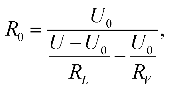 | (2) |
 | (3) |
 | (4) |
Applying the relationship of RL = RV = 10 MΩ, and the eqn (2)–(4), the resistance change rate of the gas sensor could be simplified as
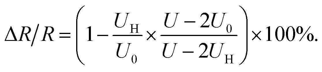 | (5) |
3. Results and discussion
The samples were prepared by using a metal-seed planting method (see the Methods for details). Fig. 2(a) schematically illustrates the procedure for planting tungsten seeds to synthesize the tungsten oxide nanoflowers. Initially, tungsten particles as metal-seeds with sizes of 3–5 μm were planted on certain regions of a quartz substrate. Then, the metal-seeds underwent a thermal oxidation, in which the substrate was heated to 900 °C and maintained at this temperature for 15 min under oxygen gas flow at 2.0 standard cubic centimeters per minute (sccm) in a vacuum; the metal-seeds were oxidized into metal oxide nanostructures. Finally, the sample underwent a natural cooling to room temperature in a vacuum. As a result, a flower-like nanostructure grew up on the region with a tungsten seed, while dense nanowires randomly grew up on the regions without a tungsten seed, as the typical scanning electron microscopy (SEM) images show in Fig. 2(b) and (c). In such a flower-like nanostructure, lots of nanowires with diameters in the range of 50–100 nm (as a nanowire shells) extended around a particle (as a nanoparticle core) in all directions to form a nanoflower. Predictably, the nanoflowers only appeared on the places where the tungsten seeds were planted. Thus, if we could control the positions of the micrometer-scale tungsten particle seeds on the substrate before the thermal oxidation, the controllable, localized growth of the nanoflowers would occur. In order to prove this point, we tried to push the tungsten particles with size in the range of 3–5 μm to the setting positions by using a microprobe under the microscopy magnification of 100 times.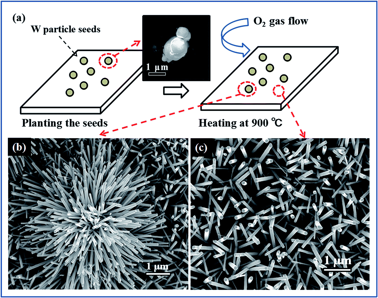 | ||
| Fig. 2 (a) Schematic diagram illustrating the procedure for planting tungsten seeds to synthesize the nanoflowers. Inset: SEM image of the metal-seeds. (b and c) SEM images of the regions with and without tungsten seed on the substrate, respectively. | ||
From our efforts above, one-dimensional (1D), two dimensional (2D) and three-dimensional (3D) patterns composed of the nanoflowers were prepared by the above synthesis methods, after the tungsten seeds were held together on a quartz substrate like the Arabic numeral one, Chinese numeral two, parallel quadrangle and “monkey” models by manual operation, as shown in Fig. 3(a–e), respectively. Although it is hard to control the position of the metal-seeds using a microprobe under the microscope, the results shown in Fig. 3 prove the feasibility of the controllable localized growth of the metal oxide nanoflowers by controlling the position of metal-seed in this method. The X-ray diffraction (XRD) spectrum of the nanoflowers, as shown in the middle section of Fig. 4, indicates that three diffraction peaks (denoted by red Miller indices) agree well with cubic W (JCPDS card no. 04-0806), and the other diffraction peaks (denoted by black Miller indices) agree with the phase of monoclinic W18O49 (JCPDS card no. 36-0101). In particular, the peak corresponding to the diffraction from the (010) plane of monoclinic W18O49 was particularly strong, which may be due to the preferred orientation along the [010] direction during the growth of tungsten oxide nanoflowers. Therefore, the as-synthesized nanoflowers should contain W and W18O49. However, a question arose as to which part of the nanoparticle core or the nanowire shell was metal W, and which was the W18O49 phase in a nanoflower structure. In order to distinguish this, another structure characterization technique with higher resolution was required to analyze these produces; therefore, scanning transmission electron microscopy (STEM) equipped with an energy dispersive X-ray spectroscopy (EDS) detector was also applied to characterize the products in this study.
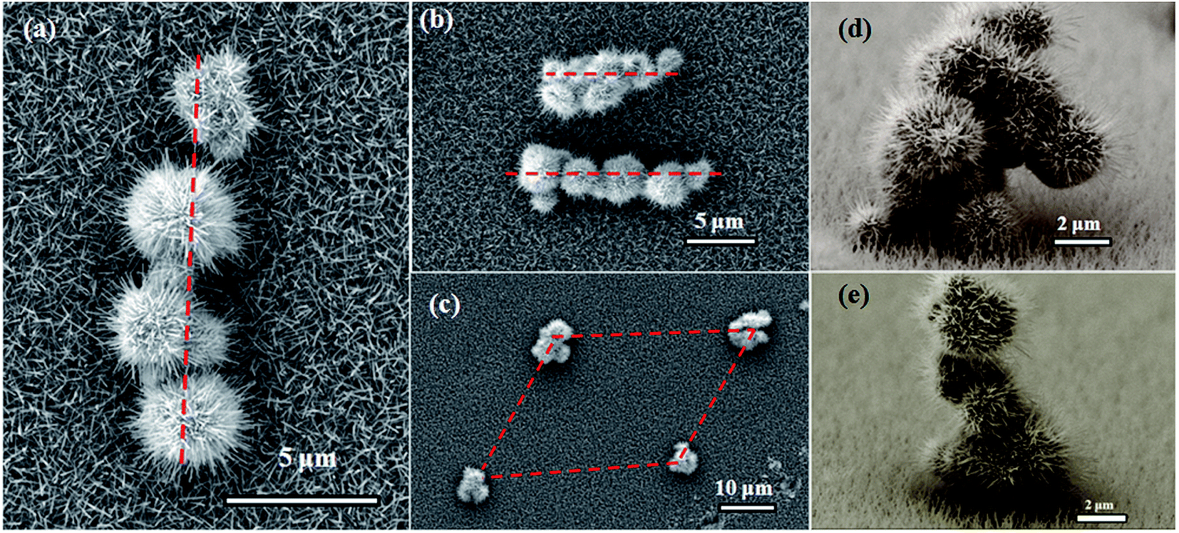 | ||
| Fig. 3 (a–e) 1D, 2D, and 3D patterns prepared via the synthesis of the nanoflowers by previously promoting the W seeds held together on quartz substrates like the Arabic numeral one, Chinese numeral two, parallel quadrangle and “monkey” models by manual operation before the thermal oxidation. | ||
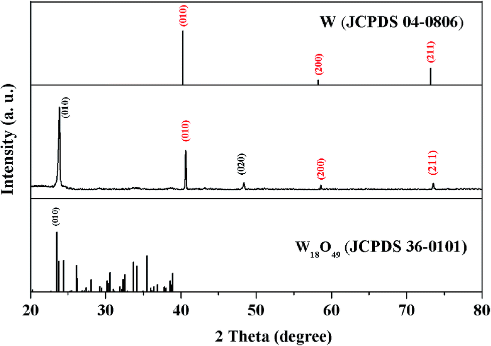 | ||
| Fig. 4 XRD spectrum of as-synthesized nanoflowers (middle section): the diffraction peaks agreeing with W (JCPDS: 04-0806) and W18O49 (JCPDS: 36-0101) are denoted by red and black Miller indices, respectively. | ||
Fig. 5 shows a typical high resolution transmission electron microscopy (HRTEM) image of a nanowire segment in the nanoflower, and its inset clearly shows that the interplanar spaces along the growth direction of the nanowire was 0.373 nm, agreeing with the interplanar pace along the direction of [010] in the W18O49 phase in the XRD test of Fig. 4. Thus, the nanowire shell should be assigned to the W18O49 phase. However, because the nanoparticle core was so thick that the transmission electrons could not transmit through it, the HRTEM image of the core was unobtainable. Its phase could be identified by the energy dispersive X-ray spectroscopy (EDS) mapping analysis of elements W and O. As shown in Fig. 6(b) and (c), both W and O appeared in the core and the nanowires shell, but W element was concentrated in the core while O element mainly appeared in the nanowire shell. This can be better illustrated by EDS line scanning, as shown in Fig. 6(d) and (e): the EDS line scan curves indicate that the profile of W showed a broad peak, which was located at the center of the particle core, while the profile of O showed higher intensity on both sides of the particle core. These results could be analysed as follows: firstly, since the particle core was enclosed by the nanowires and the nanowires belonged to the W18O49 phase, O element not only appeared on both sides, but also appeared on the particle core due to the EDS sign from the nanowires, which enclosed the core. Secondly, the particle core was mainly composed of W element, and the XRD results in Fig. 4 showed there was a cubic W phase in the nanoflowers. Thus, it is reasonable to believe that the W particles could not be totally oxidized into W18O49 during the thermal oxidation, and the core remained in the cubic W phase.
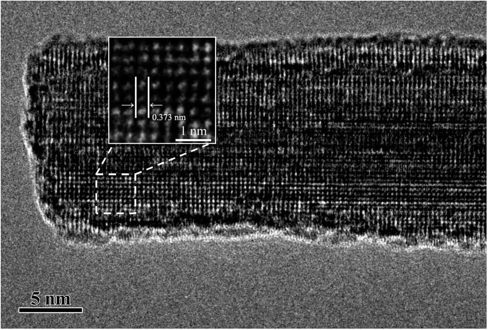 | ||
| Fig. 5 Typical HRTEM image of a nanowire segment in the nanoflower structure. Inset: enlarged image of the white-dashed-square region. | ||
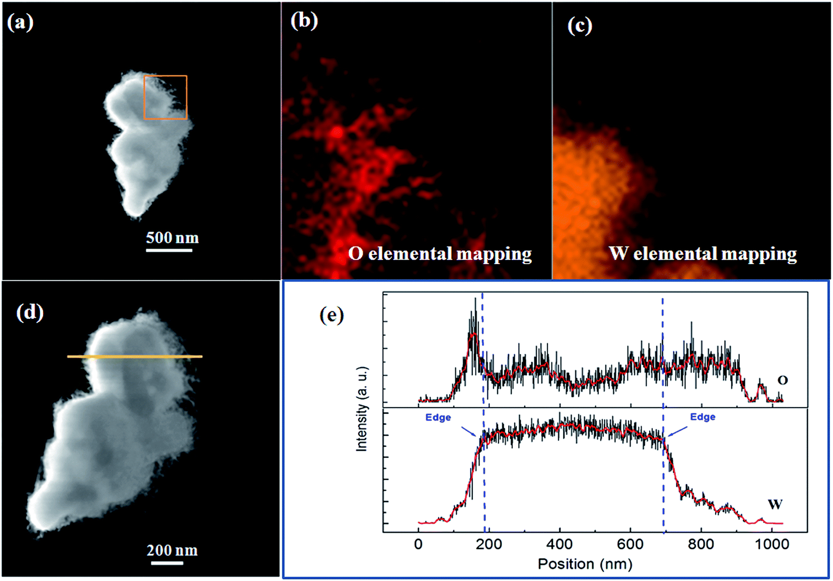 | ||
| Fig. 6 (a) Dark-field STEM image of a tungsten oxide nanoflower. (b and c) EDS element mapping images show O and W element profiles from the region denoted by an orange square in (a). (d) Dark-field STEM image of a tungsten oxide nanoflower showing the position of EDS line scanning. (e) EDS line scan curves indicating the elements O and W, respectively. The dotted lines mark the edges of the nanoparticle core in the nanoflower. | ||
Another question arose as to how this W–W18O49 core–shell nanoflower grew during the thermal oxidation. In order to reveal this, we recorded the growth process by varying the heat-retention time in the thermal oxidation. As the typical cross-sectional view SEM images in Fig. 7(a–d) show, W seeds with the diameters in the range of 2–5 μm were planted at the substrate. At the heat-retention time of 5 minutes, the nanowires grew on the surface of W seeds and covered them to form the flower-like nanostructures as shown in Fig. 7(b). As the heat-retention time increased from 5 minutes to 30 minutes, more and more new nanowires grew up and the former nanowires got longer on the surface of each W seed, and simultaneously, the W seed gradually became smaller (as shown in Fig. 7(a–c)). When the heat-retention time reached to 30 minutes in particular, the nanoflower structures had collapsed, due to the vanishing of W seeds and missing core support. The structural changes of the prepared nanoflower with the increase of the heat-retention time was also investigated by the XRD patterns. As shown in Fig. 7(e), all the crystal structures of the products could be well indexed to cubic W (JCPDS card no. 04-0806) and monoclinic W18O49 (JCPDS card no. 36-0101), and these results clearly indicate that with the increase of the heat-retention time, the phase of the product gradually changed from the original cubic W into final monoclinic W18O49. Since the nanowires with high crystallinity had been synthesized even at the beginning of the heat-retention time of 5 minutes, the diffraction peaks from monoclinic W18O49 had been strong enough at the beginning. However, as can be seen from Fig. 7(e), with the heat-retention time increasing, all the diffraction peaks indexed to cubic W gradually decreased in intensity, and then totally disappeared at 30 minutes, corresponding to the disappearance of the particle core as the SEM result in Fig. 7(d). Simultaneously, the intensity of the diffraction peaks indexed to monoclinic W18O49 increased with the heat-retention time. These results clearly reveal the process for the oxidation from W metal-seeds into W18O49 nanowires with the increase of the heat-retention time, and the W–W18O49 core shell nanoflowers were just the intermediate products at a suitable heat-retention time.
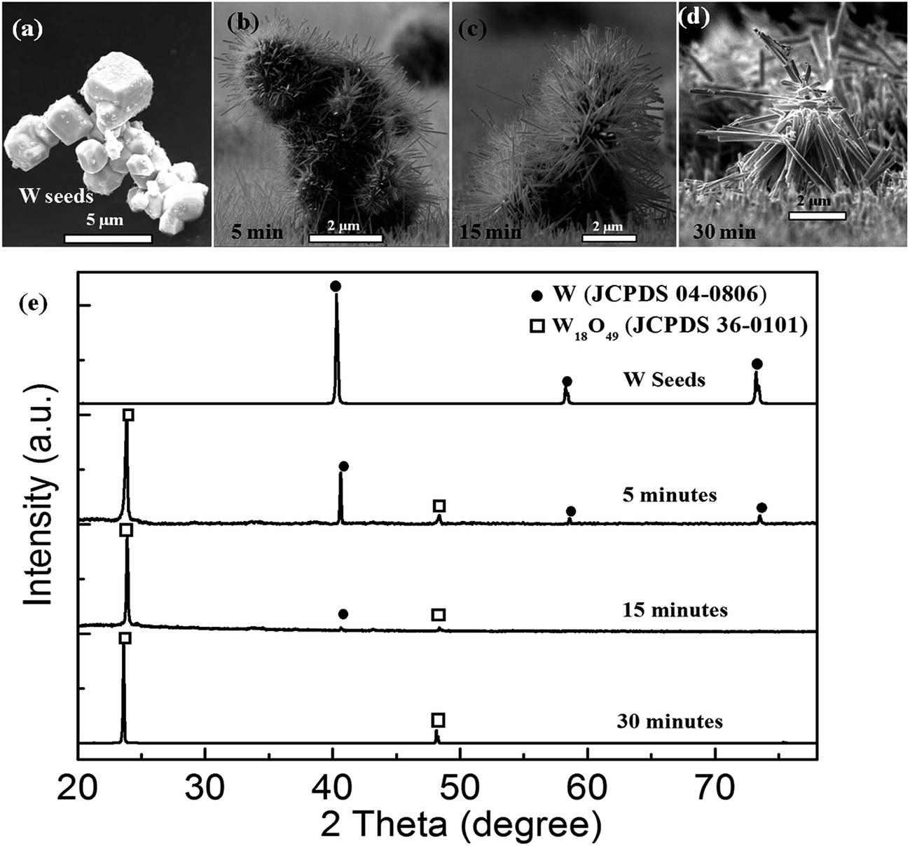 | ||
| Fig. 7 (a) SEM image showing the typical cross-sectional view of the W seeds. (b–d) SEM images showing the cross-sectional view of products prepared at the heat-retention time of 5, 15 and 30 minutes in our experiments, respectively. (e) XRD spectra for the W seeds and the products prepared at the heat-retention time of 5, 15 and 30 minutes in our experiments, respectively. | ||
The growth model of the W–W18O49 core shell nanoflowers is discussed in more detail below. Without any catalyst, the synthesis process was a thermal evaporation process, which was proposed as a vapor–solid (VS)33 growth process in this case. W particle seeds with a melting point of more than 3000 °C could not be gasified around the temperature of 800 °C in our synthesis process, and thus the vapor in the VS growth model should be tungsten oxide vapor not tungsten vapor. As shown in Fig. 7(a–d), the surface layer of the W particle seeds would be oxidized into tungsten oxide by the introduced oxygen under vacuum, and then the solid tungsten oxide could be evaporated into tungsten oxide vapor at 800 °C or above. The new exposed W on the particle surface would be also oxidized into tungsten oxide and then become tungsten oxide vapor. Dependent on all the experimental findings and the analysis above, the growth process was proposed as shown in Fig. 8. (1) As the thermal oxidation started, the W particle seeds began to be oxidized into tungsten oxide by the introduced oxygen in vacuum. (2) The thin tungsten oxide layer could then easily become vapor above 800 °C, and the vapor would escape from the particle seeds, to be cooled to solid state tungsten oxide overhead and then deposited back on the surfaces of the particle seeds or on the surface of the substrate. (3) When the temperature decreased to lower than 800 °C, the evaporation would stop, and the deposition of tungsten oxide should play two roles. One role is to deposit on the surface of the substrate to form W18O49 nanowires at the regions without W particle seed, and the other role is to regenerate W18O49 on W particle seed surfaces and connect them to form the nanoflower structures. With the process of evaporation and deposition, the W particle seed became progressively smaller and ultimately ran out. In the end, the collapse of the nanoflower structure suggests its inability to sustain and dominate as a core.
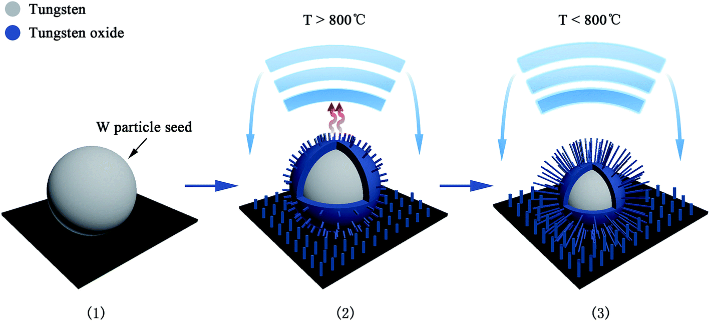 | ||
| Fig. 8 Proposed growth process for the formation of the nanoflower structure (see text for details). | ||
As is well-known, WO3 has been highly expected to be a novel sensing material because of its high gas-sensing properties.20–28 With the high specific surface area of the nanoflowers in this study, the film composed of WO3 nanoflowers should be expected to have better gas sensing performance, since the WO3 nanoflowers could be easily achieved by annealing W–W18O49 nanoflowers in air in our experiments. In order to prove this, we fabricated the gas sensor device based on WO3 nanoflowers film. Fig. 9 gives a schematic illustration of the fabrication process. It is worth pointing out that a layer composed of tungsten oxide nanowires was inserted between the nanoflowers and the substrate by a similar thermal evaporation (see the Methods for details) in order to increase the contact area and improve the adhesive force between the nanoflowers and the substrate. The fabrication included six main steps as shown in Fig. 9(a): (I) the quartz substrate covered the W particles, which had been flatted on the bottom of a tungsten boat. (II) Tungsten oxide nanowires grew on the substrate and connected with the W particles in the thermal evaporation (details in the Methods section). (III) The substrate was then turned over, and the W particles remained on the top layer, in the method of metal-seed planting above, to synthesize the nanoflowers on the surfaces of the W particles. (IV) The products after step (III) were annealed in air for more than 3 hours at 500 °C to make sure the products including the nanowires and nanoflowers were in the monoclinic WO3 phase (see Fig. S1 in the ESI†). (V) Pt nanoparticles with sizes in the range of 2–5 nm were used as a catalyst layer to coat the surfaces of the WO3 nanoflowers by a sputtering method (which was described in our previous work34–36), and were named Pt–WO3 nanoflowers. (VI) Finally, two metal electrodes (i.e., Pt electrodes) were fabricated on both sides of the nanoflower film by using a baffle mask with a spacing of about 5.0 mm in magnetron sputtering (see the Methods for details). The SEM images in Fig. 9(b–d) show the outcomes of the key steps of the device fabrication respectively, in agreement with our expected results.
 | ||
| Fig. 9 (a) Schematic illustration of the fabrication process of the gas sensor device based on the nanoflower film. (b–d) SEM images showing the outcomes at the key fabrication steps of (II), (III), and (VI), respectively. | ||
The gas sensitive properties of the device were tested in a hydrogen sensor testing system (for details see the Experimental section 2.6). The gas sensing activity of the Pt–WO3 nanoflower film was investigated by introducing different concentrations of H2 at room temperature. From the inset of Fig. 10(a), one can see that the surface sensing material of the sensor was mainly composed of the flower-like nanostructures, in whose material fabrication stage the density of the tungsten particles was intentionally increased. The time response curve for the voltage across the sensor in Fig. 10(b) shows that when the sensor was exposed to hydrogen gas, its voltage dropped to a stable value in 20 min for the low hydrogen concentration, but continued to drop even after 30 min for the high hydrogen concentration, as shown in Fig. 10(c) and (d). For comparison with the falling range from 50 to 5000 ppm on the same time scale, and to avoid the destruction of the WO3 nanostructures, which may be induced by the long time testing under the high hydrogen concentration environment, we interrupted the voltage falling process at 45 min in the cases of 3000 and 5000 ppm. This destruction of the sensing nanomaterial induced by high hydrogen concentration could be seen from the recovery process in air, in which the recovered voltage exceeded the initial value (denoted by a red virtual level in Fig. 9(b)), indicating that the recovered resistance of the sensors was larger than the initial resistance R0. This may be attributed to the hydrogen injection into the lattice structure and the formation of the localized water molecules and the oxygen vacancies in the lattice structure (these models have been proposed in our previous work25,34), destroying the microstructure of the nanoflowers in an environment of high hydrogen concentration, which has also been observed recently by our group in the layered α-MoO3 materials;37 however, the exact answer needs to be determined in future work.
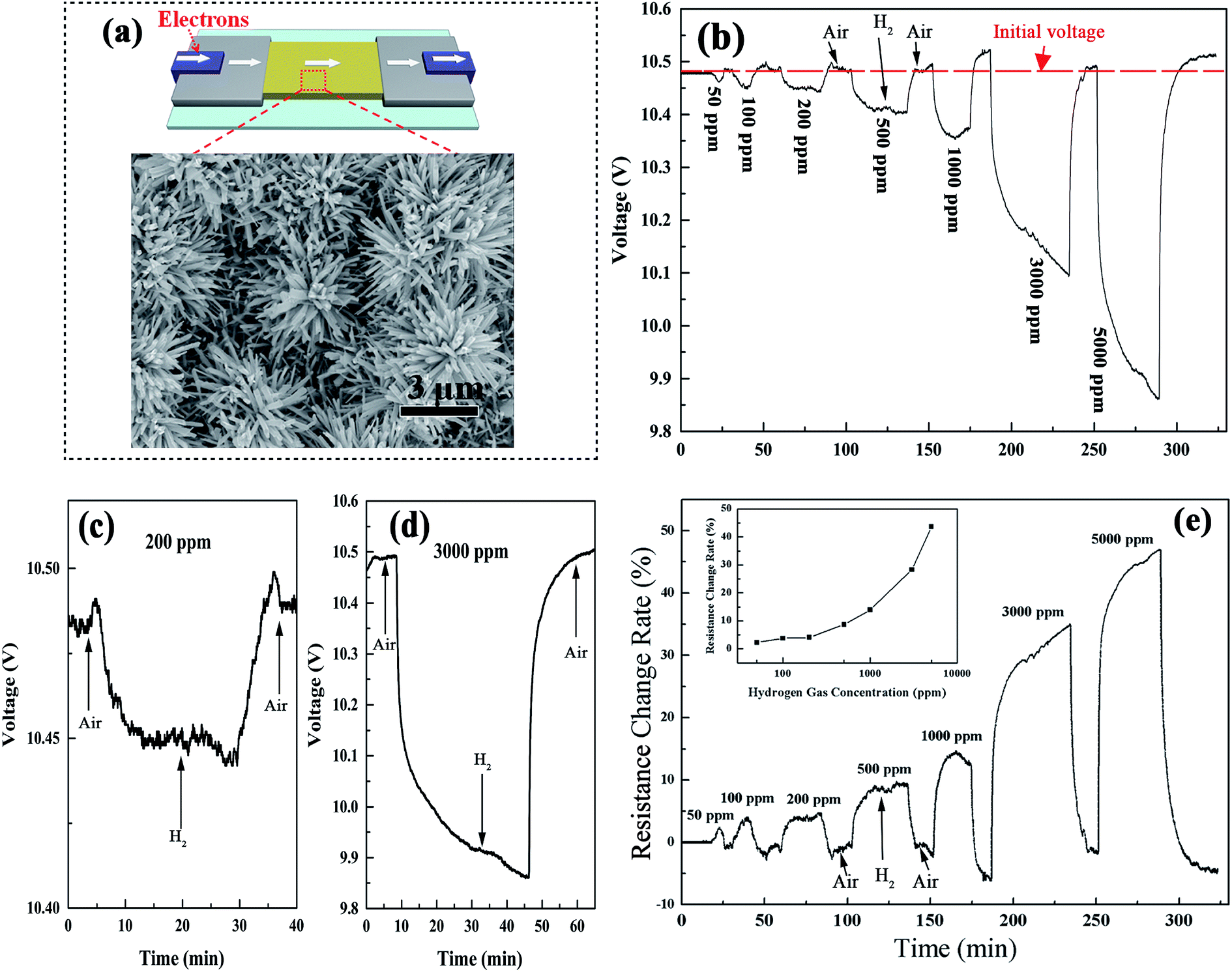 | ||
| Fig. 10 (a) Schematic illustration of the gas sensor device based on the Pt–WO3 nanoflower film. Inset: top-view SEM image for the nanoflower film. (b) The time response curve for the voltage across the sensor under the different hydrogen concentrations at room temperature. (c and d) The enlarged time response curves from part (b) at low and high hydrogen concentrations, respectively. (e) The corresponding resistance change rate curve obtained from the relationship of eqn (5). | ||
The typical hydrogen response curve of the device is shown in Fig. 10(e), in which the sensor response, also known as the relative resistance change,38,39 could be calculated by eqn (4) and (5) in the Experimental section. The relationship between the sensor response and H2 concentration nearly satisfied an exponential function as the hydrogen concentration increased. For comparison with other tungsten oxide phases, the hydrogen response curves for W18O49 nanowires, W–W18O49 nanoflowers, WO3 nanowires, WO3 nanoflowers, and Pt–WO3 nanowire films have also been tested under the same conditions at room temperature (see Fig. S2 in the ESI†). In addition to a light and unstable response in Pt–WO3 nanowires, the others had no response to 50–5000 ppm hydrogen at room temperature. Thus, among them, the Pt–WO3 nanoflowers have a relatively outstanding performance.
Compared to the homogeneous metal oxide (MOX) sensors, two advantages for our devices should be pointed out here. Firstly, most of the homogeneous MOS sensors would become saturated under high hydrogen concentration detection in industrial productions.9,40 However, the saturation effect was not observed in our devices, even when the hydrogen concentration was greater than 5000 ppm. This is due to the high specific surface area of the nanoflowers, which enable them to adsorb enough hydrogen molecules. Secondly, MOX sensors need high operating temperatures (approximately 300 °C or greater) to obtain stable and measurable conductivities,8,9 and in our previous work, the operating temperature was dropped to near 100 °C by using quasi-one-dimensional WO3 nanowire film as a sensing unit.25 Although the stability for the detection of more than 5000 ppm hydrogen needs to be improved in our further work, the sensors have a relatively stable sensing performance at hydrogen concentrations less than 5000 ppm at room temperature (see Fig. S3 ESI†). After 50 cycle tests, the sensors still had a stable response cycle curve in a gas atmosphere, switching between 2000 ppm hydrogen and air.
4. Conclusion
In summary, the W–W18O49 nanoflowers were controllably synthesized on the pre-designed regions of the substrate by a metal-seed planting method. The nanoflowers were composed of a nanowire shell and a nanoparticle core, and their structures were assigned to monoclinic W18O49 and cubic W phases respectively, based on the material characterization results of SEM, XRD, and STEM. The process for the metal-seed W particles growing into the nanoflowers was facilitated by varying the heat-retention time in the thermal oxidation, and the results revealed that the cores of the nanoflowers became smaller until they disappeared, while the nanowires on the surfaces of the cores grew with the heat-retention time. The growth model of the W–W18O49 core shell nanoflowers was also proposed in this study, in which the surface layers of W seeds were oxidized into tungsten oxide vapor and the W seeds became smaller during the thermal oxidation to act as the cores of the nanoflowers. The tungsten oxide vapor followed the VS model and was deposited back on the surfaces of the W seeds to form the nanowire shells in the nanoflower structures. Finally, the hydrogen gas sensor based on the Pt–WO3 nanoflower film (which was obtained by annealing W–W18O49 nanoflower film and coated with Pt nanoparticles) was fabricated and its gas sensing test showed that it had an effective and high sensing performance at room temperature.Acknowledgements
The authors gratefully acknowledge the financial support of the projects from the National Natural Science Foundation of China (Grant No. 51402218), Guangdong Natural Science foundation for Distinguished Young Scholar (Grant No. 2015A030306031), Guangdong Natural Science foundation (No. 2014A030313622), Innovative Research Team (Grant No. 2015KCXTD027) and Training Program for Outstanding Young Teachers in University of Guangdong (Grant No. YQ2015160), and Science Foundation for Young Teachers of Wuyi University (Grant No. 2013zk05, and 2014td01).References
- Y. Zheng, Y. Jiao, L. H. Li, T. Xing, Y. Chen, M. Jaroniec and S. Z. Qiao, ACS Nano, 2014, 8, 5290–5296 CrossRef CAS PubMed.
- S. Dutta, J. Ind. Eng. Chem., 2014, 20, 1148–1156 CrossRef CAS.
- S. Cao and K. Alanne, Appl. Energy, 2015, 158, 568–583 CrossRef CAS.
- Q. Weng, X. Wang, C. Zhi, Y. Bando and D. Golberg, ACS Nano, 2013, 7, 1558–1565 CrossRef CAS PubMed.
- H. P. Veluswamy, R. Kumar and P. Linga, Appl. Energy, 2014, 122, 112–132 CrossRef CAS.
- J. F. Hull, Y. Himeda, W. Wang, B. G. Hashiguchi, R. A. Periana, D. J. Szalda, J. T. Muckerman and E. Fujita, Nat. Chem., 2012, 4, 383–388 CrossRef CAS PubMed.
- See: http://www1.eere.energy.gov/hydrogenandfuelcells/mypp/pdfs/safety.pdf, accessed 18.01.10.
- W. J. Buttner, M. Post, R. Burgess and C. Rivkin, Int. J. Hydrogen Energy, 2011, 36, 2462–2470 CrossRef CAS.
- V. Aroutiounian, Int. J. Hydrogen Energy, 2007, 32, 1145–1158 CrossRef CAS.
- E. Sennik, Z. Colak, N. Kilinc and Z. Z. Öztürk, Int. J. Hydrogen Energy, 2010, 35, 4420–4427 CrossRef CAS.
- Z. Wang, Y. Hu, W. Wang, X. Zhang, B. Wang, H. Tian, Y. Wang, J. Guan and H. Gu, Int. J. Hydrogen Energy, 2012, 37, 4526–4532 CrossRef CAS.
- I. H. Kadhim and H. A. Hassan, J. Electron. Mater., 2017, 46, 1419–1426 CrossRef CAS.
- H. Zheng, J. Z. Ou, M. S. Strano, R. B. Kaner, A. Mitchell and K. Kalantarzadeh, Adv. Funct. Mater., 2011, 21, 2175–2196 CrossRef CAS.
- M. V. Limaye, J. Chen, S. Singh, Y. Shao, Y. Wang, C. Pao, H. M. Tsai, J. Lee, H. J. Lin, J. Chiou, M. Yang, W. Wu, J. Chen, J. Wu, M. Tsai and W. Pong, RSC Adv., 2014, 4, 5036–5045 RSC.
- X. Guo, X. Qin, Z. Xue, C. Zhang, X. Sun, J. Hou and T. Wang, RSC Adv., 2016, 6, 48537–48542 RSC.
- Z. Zhao and M. Miyauchi, Angew. Chem., 2008, 47, 7051–7055 CrossRef CAS PubMed.
- Y. Tian, S. Cong, W. Su, H. Chen, Q. Li, F. Geng and Z. Zhao, Nano Lett., 2014, 14, 2150–2156 CrossRef CAS PubMed.
- Y. Tian, W. Zhang, S. Cong, Y. Zheng, F. Geng and Z. Zhao, Adv. Funct. Mater., 2015, 25, 1–7 CrossRef.
- C. Zhao, S. Z. Deng, N. S. Xu and J. Chen, RSC Adv., 2015, 5, 70059–70063 RSC.
- C. Hyeonsik, Y. S. Jae, D. L. Jae, M. J. Jung and L. Sohee, J. Korean Phys. Soc., 2009, 55, 2693–2696 CrossRef.
- J. Y. Shim, J. D. Lee, J. M. Jin, H. Cheong and S. Lee, Sol. Energy Mater. Sol. Cells, 2009, 93, 2133–2137 CrossRef CAS.
- T. Samerjai, N. Tamaekong, C. Liewhiran, A. Wisitsoraat, A. Tuantranont and S. Phanichphant, Sens. Actuators, B, 2011, 157, 290–297 CrossRef CAS.
- S. S. Kalanur, I. Yoo, Y. Lee and H. Seo, Sens. Actuators, B, 2015, 212, 411–417 CrossRef.
- L. F. Zhu, J. C. She, J. Y. Luo, S. Z. Deng, J. Chen, X. W. Ji and N. S. Xu, Sens. Actuators, B, 2011, 153, 354–360 CrossRef CAS.
- J. Y. Luo, X. X. Chen, W. D. Li, W. Y. Deng, W. Li, H. Y. Wu, L. F. Zhu and Q. G. Zeng, Appl. Phys. Lett., 2013, 102, 113104 CrossRef.
- S. Kabcum, D. Channei, A. Tuantranont, A. Wisitsoraat, C. Liewhiran and S. Phanichphant, Sens. Actuators, B, 2016, 226, 76–89 CrossRef CAS.
- N. M. Vuong, D. Kim and H. Kim, Sens. Actuators, B, 2015, 224, 425–433 CrossRef.
- Q. Xiang, G. F. Meng, H. Zhao, Y. Zhang, H. Li, W. J. Ma and J. Q. Xu, J. Phys. Chem. C, 2010, 114, 2049–2055 CAS.
- F. E. Annanouch, Z. Haddi, M. Ling, F. Di Maggio, S. Vallejos, T. Vilic, Y. Zhu, T. Shujah, P. Umek, C. Bittencourt, C. Blackman and E. Llobet, ACS Appl. Mater. Interfaces, 2016, 8, 10413–10421 CAS.
- M. Horprathum, T. Srichaiyaperk, B. Samransuksamer, A. Wisitsoraat, P. Eiamchai, S. Limwichean, C. Chananonnawathorn, K. Aiempanakit, N. Nuntawong, V. Patthanasettakul, C. Oros, S. Porntheeraphat, P. Songsiriritthigul, H. Nakajima, A. Tuantranont and P. Chindaudom, ACS Appl. Mater. Interfaces, 2014, 6, 22051–22060 CAS.
- F. Chávez, G. F. Pérez-Sánchez, O. Goiz, P. Zaca-Morán, R. Peña-Sierra, A. Morales-Acevedo, C. Felipe and M. Soledad-Priego, Appl. Surf. Sci., 2013, 275, 28–35 CrossRef.
- A. Nikfarjam, A. Fardindoost and S. Irajizad, Polymers, 2013, 5, 45–55 CrossRef.
- Z. W. Pan, Z. R. Dai and Z. L. Wang, Science, 2001, 291, 1947–1949 CrossRef CAS PubMed.
- J. Y. Luo, S. Z. Deng, Y. Tao, T. F. L. Zhao, L. F. Zhu, L. Gong, J. Chen and N. S. Xu, J. Phys. Chem. C, 2009, 113, 15877–15881 CAS.
- S. Chen, J. Luo, H. Tan, J. H. Chen, S. Deng and N. Xu, Sens. Actuators, B, 2012, 173, 824–832 CrossRef CAS.
- J. Y. Luo, W. Li, F. Chen, X. X. Chen, W. D. Li, H. Y. Wu, J. Y. Gao and Q. G. Zeng, Sens. Actuators, B, 2014, 197, 81–86 CrossRef CAS.
- W. G. Xie, M. Z. Su, Z. B. Zheng, Y. Wang, L. Gong, F. Y. Xie, W. H. Zhang, Z. Luo, J. Y. Luo, P. Y. Liu, N. S. Xu, S. Z. Deng, H. J. Chen and J. Chen, ACS Nano, 2016, 10, 1662–1670 CrossRef CAS PubMed.
- C. Wu, G. Jiang, C. Chiu, P. J. Chong, C. Jeng, R. Wu and J. Chen, Sens. Actuators, B, 2015, 209, 906–910 CrossRef CAS.
- L. Zhu, Y. Jia, G. Gai, X. Ji, J. Luo and Y. Yao, Sens. Actuators, B, 2014, 190, 134–140 CrossRef CAS.
- T. Hubert, L. Boonbrett, G. D. Black and U. Banach, Sens. Actuators, B, 2011, 157, 329–352 CrossRef.
Footnote |
| † Electronic supplementary information (ESI) available. See DOI: 10.1039/c7ra03006a |
| This journal is © The Royal Society of Chemistry 2017 |