
 Open Access Article
 This Open Access Article is licensed under a
 Creative Commons Attribution 3.0 Unported Licence
The importance of annealing and stages coverage on the epitaxial growth of complex oxides on silicon by pulsed laser deposition
Daniel Diaz-Fernandez *a,
Matjaž Spreitzera,
Tjaša Parkelja,
Janez Kovačb and
Danilo Suvorova
*a,
Matjaž Spreitzera,
Tjaša Parkelja,
Janez Kovačb and
Danilo Suvorova
aAdvanced Materials Department, Jožef Stefan Institute, Jamova cesta 39, 1000 Ljubljana, Slovenia. E-mail: daniel.diaz@ijs.si
bDepartment of Surface Engineering and Optoelectronics, Jožef Stefan Institute, Teslova ulica 30, 1000 Ljubljana, Slovenia
First published on 8th May 2017
Abstract
The integration of epitaxial complex oxides with Si represents an invaluable opportunity for the creation of novel devices with logic and sensing capabilities, both implemented in the same chip. In this work, Pulsed Laser Deposition (PLD) is used to grow epitaxial ultra-thin (3–4 nm) SrTiO3 (STO) layers on Si(001), showcasing the possibilities of this technique for the growth of templates for the integration of complex oxides with Si. Our procedure involves the growth of a 1/2 monolayer (ML) of Sr buffer layer on the reconstructed Si(001) surface by PLD, the deposition of STO in inert Ar atmosphere, and latter oxidation and crystallization phases. The optimization of STO deposition, oxidation, and crystallization parameters proves to be essential for the improvement of the layer's quality. It has been found that the minimization of the thermal budget during the crystallization phase increases the interface sharpness, but a minimum temperature is needed for a proper densification of the STO layer. A coverage of 2 ML before every crystallization and oxidation phases was determined as the best balance between the critical thickness, minimization of the thermal budget, and a proper coverage of the buffer layer, which prevents its reactions with the Sr/Si surface. These results improve the general knowledge and understanding of metal oxide/silicon heterojunctions, and represent a solid stepping stone for the growth of high-quality thin STO templates on Si by PLD.
1 Introduction
The field of the growth of epitaxial complex oxides on Si has seen a dramatic rise in interest since the breakthrough achieved by McKee et al. on the epitaxial growth of SrTiO3 (STO) on Si(001) 18 years ago.1 However, even after almost 20 years of research, the growth of this family of materials on silicon is still not properly understood. Many methods and procedures have been developed in order to achieve the integration of STO and other complex oxides on Si, but the most common route implies the removal of the amorphous SiO2 surface layer via Sr or SrO-induced deoxidation,2–4 wet chemical processing5,6 or flash annealing in UHV conditions;7 the growth of a buffer layer in order to minimize the lattice mismatch and passivate the surface,8,9 and the overgrowth of the complex oxide itself. The most used and researched deposition technique for these growths is Molecular Beam Epitaxy (MBE). However, the low deposition rate, usage only of elemental sources and flux monitoring issues makes it an inappropriate tool from the industrial point of view. In this work, we intend to showcase the use of Pulsed Laser Deposition (PLD) for overcoming these issues and deliver high-quality oxide samples, using STO as our example material. STO is by far the most studied of this family of materials, because its crystalline properties (perovskite cubic structure, space group Pm![[3 with combining macron]](https://www.rsc.org/images/entities/char_0033_0304.gif) m, lattice constant: 3.905 Å) makes it a perfect template for the epitaxial overgrowth of other complex oxides with ferroelectric, ferromagnetic, piezoelectric and high-T superconductivity properties.
m, lattice constant: 3.905 Å) makes it a perfect template for the epitaxial overgrowth of other complex oxides with ferroelectric, ferromagnetic, piezoelectric and high-T superconductivity properties.
The two key challenges lie in obtaining an adequate stoichiometry and a good sharpness of the oxide/silicon interface. The first can be overcome by optimizing the laser parameters, such as the fluency, frequency and laser spot size,10 but the minimization of the interface reactions can be more difficult, since the layers grown at room temperature are usually amorphous,11 and heating during or after the deposition is required for the crystallization of the deposited material, which usually leads to the appearance of amorphous silicate phases.12 A buffer layer is commonly deposited in the clean silicon surface before the oxide deposition, both as a way of minimizing the lattice mismatch, and to passivate the highly reactive silicon surface. However, in the growth of the first 5–15 ML, issues like oxygen diffusion into the oxide/Si interface and proper coverage of the buffer layer become critical, and inadequate growth parameters can lead to damage of the buffer layer, an appearance of amorphous interface phases, and a decrease of the overall properties of the oxide layer. The procedures developed for the growth of these oxides are therefore commonly multi-staged, with the deposition of the first monolayers of the oxide in inert atmosphere or low O2 conditions, so the oxidation of the interface is prevented; and the rest in higher O2 pressure, so a correct stoichiometry is achieved.13–15
In this paper, the influence of the deposition and oxidation stages coverages and the annealing procedure on the physical and structural properties of ultra-thin STO layers on Si will be shown. In situ Reflection High-Energy Electron Diffraction (RHEED) is used for studying real-time changes in the crystallinity of the samples, and ex situ Atomic Force Microscopy (AFM), X-ray Photoelectron Spectroscopy (XPS) and X-Ray Reflectivity (XRR) are used for characterizing the interface properties, and the STO layer morphology, composition and thickness.
2 Experimentals
2.1 Equipment, materials and techniques
The samples were grown in a custom pulsed-laser deposition chamber (Twente Solid State Technology, Netherlands) coupled with in situ high-pressure RHEED (Staib Instruments, Germany) for real-time structural measurements, and two lasers: an IR laser (coherent, λ: 800–820 nm) used for heating, and a Kr–F excimer laser (λ: 248 nm, 25 ns, coherent) used for pulsed ablation. The temperature was measured with a pyrometer (IMPAC, 1.45–1.8 μm). Before every experiment, the chamber was baked, and the base pressure was around 8 × 10⁻⁹ mbar. Commercial p-type Si(001) substrates (B-doped, 1–30 Ω cm, Si-Mat, Germany, 5 mm × 5 mm) and sputtering STO and Sr targets (purity: 99.9+%) were used for the growths.The thickness of the samples was measured ex situ by XRR, using an Empyrean diffractometer with PIXCel3D detector, (PanAlytical, Netherlands). On the incident side, a programmable divergence slit with a 1/16° aperture was used, along with a 1/16° fixed anti-scatter slit, and a fixed incident beam mask of 2 mm. On the diffracted side, a parallel-plate collimator with an acceptance angle of 0.27° and a PIXCel3D detector in the receiving-slit mode (all channels active) were used. The XRR spectra were acquired in the ω–2θ mode in the range from 0.1 to 5°, with a 0.005° step size and 11 s per step. The simulation of obtained curves was performed using the X'Pert Reflectivity software and a segmented fit procedure. The error in the parameters was obtained with the Error Analysis tool implemented in the software.16
The chemical composition of the interface and STO layers was determined ex situ using an monochromatic XPS system (Physical Electronics, Inc., USA, E = 1486.6 eV) with a hemispherical analyzer (resolution: 0.3 eV) and a multichannel detection system. All the spectra were taken at take-off angles of 20, 45 and 70° (the take-off angle is defined here as the angle of the X-ray source with respect to the sample surface normal). The 20° take-off angle spectra are those presented in this work, since they allow us to explore the whole depth of the sample and interface structure (λ ∼ 3–4 nm, calculated with the TPP formula17); and the 45 and 70° spectra were used for separating the bulk components from those coming from surface contamination. The charge correction was made with respect to the adventitious C 1s component at 284.8 eV, and the fittings were performed with the software XPS Peak. The morphology of the samples was obtained with a Veeco Dimension 3100 AFM/MFM system, and the images were processed with the software WSxM.18 The root-mean-square (RMS) roughness value and relative error were obtained with three 5 μm × 5 μm images recorded in different areas of each sample.
2.2 Growth description
The deposition of STO on Si was carried out following the multi-staged process previously established in our group by Klement et al.19 It mimics previous successful MBE epitaxial growths of STO on Si,20,21 and it can be summarized in the following steps:(1) Removal of the SiO2 layer by flash annealings in UHV conditions (∼1000 °C, 10−9 mbar).
(2) Growth of a 1/2 ML Sr buffer layer by PLD.
(3) Growth of 1–4 ML of STO in an Ar atmosphere (5 × 10⁻² mbar) and room temperature.
(4) Exposure of the freshly grown STO to O2: 9.3 × 10⁻⁷ mbar, 5 min (oxidation stage).
(5) Repetition of steps (3) and (4), until a desired thickness is achieved.
(6) When enough MLs have been grown, the layer is crystallized by heating on UHV conditions (crystallization stage).
(7) Repetition of steps (3)–(5) until a thickness of 10–12 ML is achieved.
The PLD growth of STO in vacuum or inert atmosphere is inherently oxygen-deficient,22,23 but the deposition of STO in an O2 atmosphere is also not convenient in our case, given the high sensitivity of the buffer layer: it is because of this reason that separate deposition and oxidation stages are introduced. From now on, the coverage before every oxidation stage is going to be referred as “Coverage Per Oxidation” or “CovOX”, while the total coverage before the crystallization stage is going to be referred as “Coverage Per Crystallization” or “CovREC” Previous research efforts made by our group in the last two years studied the impact of parameters such as the laser fluence, substrate temperature and growth pressure, on the quality of these layers.19 It was shown that proper optimization of the laser fluence led to optimal STO stoichiometry and avoidance of large particulates formation, while an adequate argon pressure led to smoother STO layers and better crystallinity. The impact of the substrate temperature was lightly explored, but it was shown that temperatures higher than 545 °C led to interface reactions and final polycrystalline samples. Based on these previous experiments, a set of parameters was established as our default procedure, and two groups of experiments were devised around these parameters, testing the coverage per oxidation (SOX samples) and recrystallization (SREC samples), with two values both above and below the default parameters. Furthermore, two experiments were also devised for testing the crystallization process (SPR,1 and SPR,2 samples). On the first one, the same crystallization procedure used in samples SREC and SOX was followed, and the rest of conditions were taken from sample SOX,3 since it was the sample that showed the best properties, as it will be shown afterwards. In the second one, the sample was heated with the same temperature ramp until slight signs of crystallization were seen in the in situ RHEED patterns. If 545 °C were reached and no crystallization signs were observed, the sample would stay at that temperature for 15 minutes, and then it would be cooled down, effectively mimicking the original crystallization procedure. The first crystallization of sample SPR,2 was performed at 545 °C for 15 minutes, but in the subsequent crystallizations, progressively lower temperatures were necessary for the RHEED images to show some crystallization signs (500, 435, 315, and below 250 °C, respectively). The growth parameters of all these samples and experiments are summarized in Table 1.
| CovOX (ML) | CovREC (ML) | TREC (°C) | tREC (min) | CovFINAL (ML) | Sample name | |
|---|---|---|---|---|---|---|
| Default conditions | 1 | 2 | 545 | 15 | 10 | SD |
| Coverage per crystallization | 1 | 2 | 545 | 15 | 10 | SREC,1 = SD |
| 1 | 3 | 545 | 15 | 12 | SREC,2 | |
| 1 | 4 | 545 | 15 | 12 | SREC,3 | |
| Coverage per oxidation | 1/2 | 2 | 545 | 15 | 10 | SOX,1 |
| 1 | 2 | 545 | 15 | 10 | SOX,2 = SD | |
| 2 | 2 | 545 | 15 | 10 | SOX,3 | |
| Crystallization procedure | 2 | 2 | 545 | 15 | 10 | SPR,1 = SOX,3 |
| 2 | 2 | Heating stops when streaks appear in the RHEED pattern (see text for more information) | 10 | SPR,2 | ||
2.3 Experimental conditions
The substrates were first ultrasonically cleaned in acetone for 10 min, thoroughly rinsed with ethanol, and blow-dried with a N2 gun. Subsequently, they were mounted into a hollow Ta sample holder, which allowed direct heating of the substrate with the IR laser from the back, and after being inserted on the PLD chamber, they were prebaked at 630 °C for >12 h.The removal of the native SiO2 layer was carried out by flash annealings of the substrate (∼1200 °C, 1 min, maximum pressure of 3 × 10⁻⁸ mbar), with in situ RHEED monitoring of the [001] azimuth. After the second flash annealing, the deposition of the 1/2 ML Sr buffer layer was carried out using an elemental Sr target (purity 99.9%, MaTeck, Germany), which was previously preablated in vacuum before every deposition. The buffer layer material and coverage were chosen because it has been proven to be the most suitable buffer layer in terms of achieved crystallinity.24,25 The coverage was determined by in situ RHEED, monitoring the pattern change seen when the surface reconstruction of the Si(100) surface changes from (2 × 1) + (1 × 2) to a (2 × 3) reconstruction at a coverage of 1/6 ML.8,26 Afterwards, the samples were cooled down, and STO was grown using the stages already described in the previous subsection. The pressures and temperatures used in each step of the Sr and STO growth are summarized in Table 2.
| Parameter | Sr deposition | STO deposition |
|---|---|---|
| Substrate temperature (°C) | 700 | 25 |
| Deposition pressure (mbar) | 1–2 × 10⁻⁸ | 5 × 10⁻² (Ar) |
| Spot size (mm2) | 0.14 | 0.58 |
| Fluence (J cm−2) | 1 | 1.5 |
| Repetition rate (Hz) | 0.25 | 1 |
3 Results
3.1 Interface
XPS (Si 2p region) and XRR were used to explore changes in the structure and sharpness of the interface. The XPS Si 2p spectra (Fig. 1) show two main spectral features. The first one, located around 98.9 eV, and which shows a peak doublet (Si 2p3/2 and Si 2p1/2), corresponds to the bulk substrate signal. The other feature, located roughly at 101.9 eV, shows a wider peak, and corresponds to additional phases formed at the interface, such as strontium silicates or sub-stoichiometric silicon oxides.27 At a first glance, all spectra show the same basic features, except for sample SPR,2 which show a less intense silicate phase peak that, upon careful inspection, seems shifted to the left (∼101 eV). Fig. 2a shows fittings for samples SPR,1 and SPR,2 as an example, since all spectra are satisfactorily fitted using the same basic features; and they reveal that the silicate “peak” is actually composed by two contributions: one at 101.3 eV, and another at 102.4 eV. These contributions are assigned to Si2+ and Si3+ states, respectively.28 Fig. 2b to d show the normalized (with respect to the bulk substrate signal) Si2+ and Si3+ peak intensities for all the samples studied. It is clear from the data that the changes in the crystallization and oxidation coverages do not influence the intensities of these contributions. However, the intensity of both peaks, and specially that of Si3+ decreases in sample SPR,2 (Fig. 2d). The decrease in the intensity of these peaks is a clear indication that this sample has a sharper interface, and since the rest of the samples were recrystallized for longer periods of time and higher temperatures, it can be inferred that the interface sharpness improves when the thermal budget of the overall process is decreased. The different decrease ratio of these peaks suggests a different origin for these two contributions. The Si2+ peak intensity changes less with the thermal budget reduction, so it seems related to the deposition process itself (STO or Sr buffer layer). On the other hand, the more noticeable changes in the Si3+ peak intensity suggests that this contribution is more related to the crystallization process itself.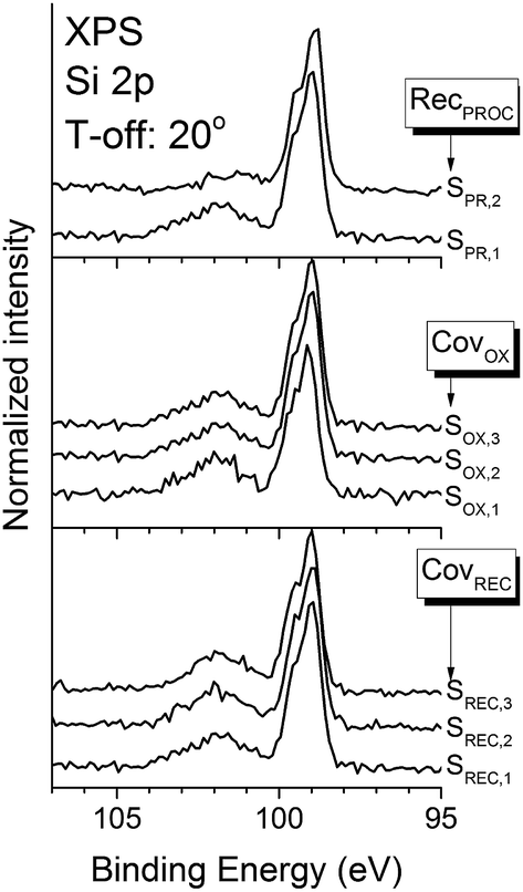 | ||
| Fig. 1 XPS spectra of the Si 2p region for all the samples studied. Take-off angle of all the spectra: 20°. | ||
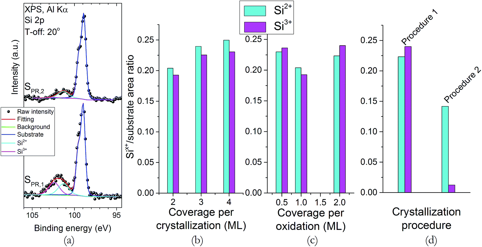 | ||
| Fig. 2 (a) XPS, Si 2p region spectra fittings for samples SPR,1 and SPR,2. (b–d) Normalized (with respect to the bulk substrate signal) intensity of the Si2+ and Si3+ contributions for all samples. | ||
The XRR spectra can be seen in Fig. 3, along with the model used for the fittings. This model assumes, aside from STO and interface layers, an additional Si layer with less density than the substrate, in order to simulate possible ion implantation due to the energetic nature of the PLD deposition.3 For the interface layer, strontium silicates (SrSiO3 and Sr2SiO4) and silicon oxides were tested: the best results were obtained using a strontium silicate, with no definite improvements found when one of them was used over the other. A model without this interface layer was also tested, but the fittings quality decreased noticeably. The results of these fittings for the interface layer can be seen in Table 3. For all samples, the density of the strontium silicate ranges from 3.8 to 4.1 g cm−3, which are close to the nominal density of both SrSiO3 and Sr2SiO4 (3.65 and 3.84 g cm−3, respectively29). The thickness ranges from 1.2 to 1.6 nm, except for sample SPR,2 which shows a thickness of around 0.9 nm. These values all agree with what has been observed by XPS, and confirm that the interface sharpness is improved once the thermal budget of the experiment is minimized.
 | ||
| Fig. 3 XRR spectra for all the samples studied in this work. | ||
| Interface layer | ||
|---|---|---|
| Sample | Thickness (nm) | Density (g cm−3) |
| SREC,1 | 1.2 ± 0.2 | 4.0 ± 0.3 |
| SREC,2 | 1.5 ± 0.1 | 3.9 ± 0.2 |
| SREC,3 | 1.6 ± 0.2 | 4.1 ± 0.3 |
| SOX,1 | 1.3 ± 0.1 | 3.8 ± 0.2 |
| SOX,2 | 1.3 ± 0.2 | 4.0 ± 0.3 |
| SOX,3 | 1.2 ± 0.1 | 3.8 ± 0.4 |
| SPR,1 | 1.2 ± 0.1 | 3.8 ± 0.4 |
| SPR,2 | 0.9 ± 0.1 | 4.0 ± 0.5 |
3.2 SrTiO3 layer
The surface crystallinity of the STO layer was examined with in situ RHEED. Previous results by our group showed that, using similar conditions, STO grows on 1/2 ML Sr/Si(100) surfaces with in-plane [110] and out-of-plane (100) orientations, which agrees with previous results on similar MBE growths of STO on Si using a Sr buffer layer.30,31 Fig. 4 shows the RHEED patterns obtained after the final crystallization for the SREC and SOX samples. Results from sample SPR,2 are not presented, since the crystallization is stopped once the slightest hint of streaks is observed, which makes the RHEED data from that sample not directly comparable with the rest. Samples SREC and SOX show streaks in both azimuths, which means that the growth has a high degree of epitaxy, and that the orientations of these samples are congruent with the consulted literature and with our previous results. The [110] azimuth shows some streak modulation, which is consistent with previous results for epitaxial MBE growths of STO on Si27 but indicates that the growth on this direction is not as smooth as in the [100] azimuth.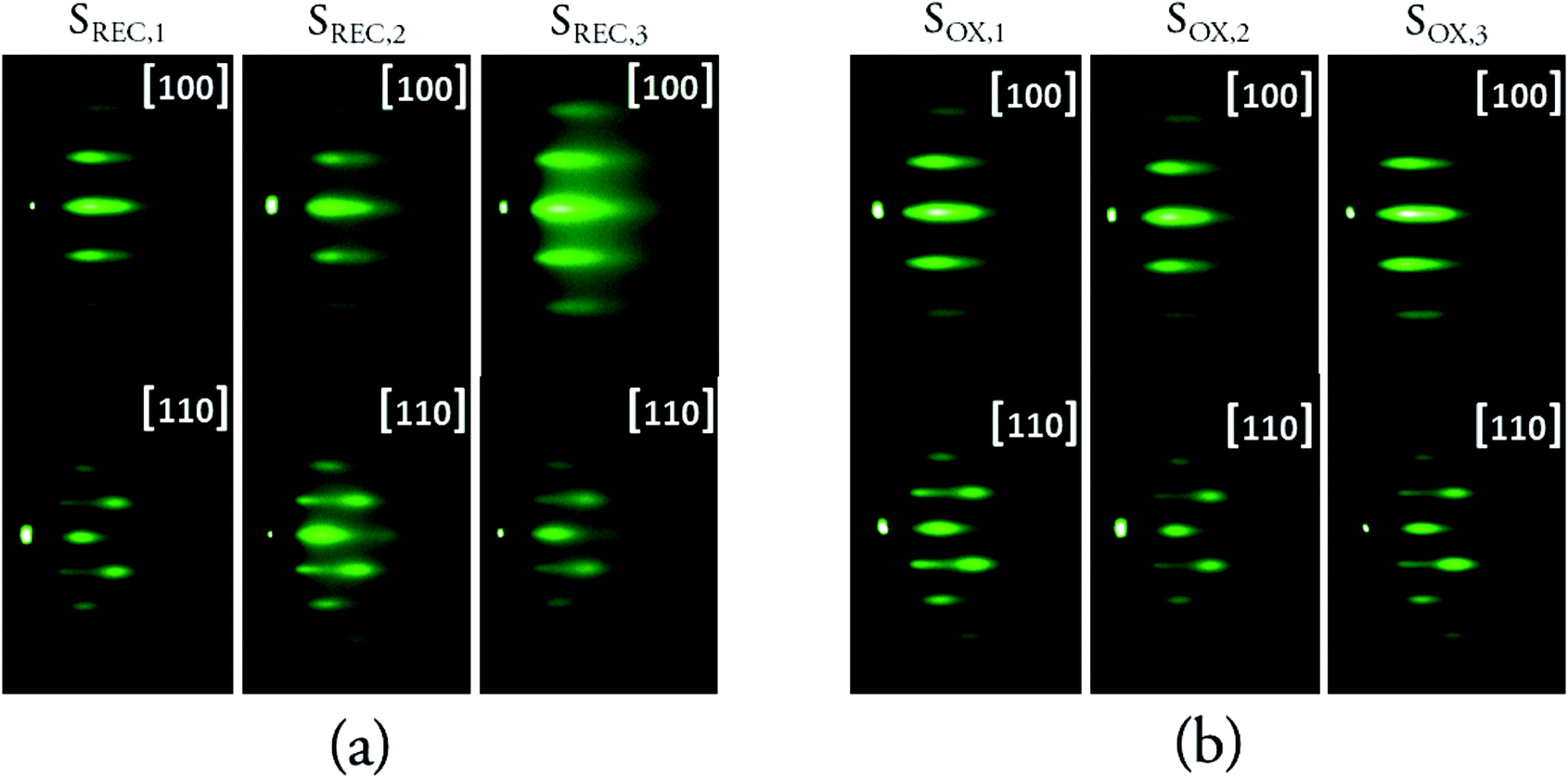 | ||
| Fig. 4 RHEED profiles for the SREC and SOX samples, after the final crystallization. The respective coverages can be found in Table 1. | ||
In order to extract more information from these patterns, line profiles were taken for the [100] azimuth, and the properties of the [00] streak were assessed via Gaussian fittings. The results for the FWHM of this streak for each crystallization coverage of samples SREC and SOX are shown on Fig. 5, along with the temperature when the streaks start to be slightly visible in the RHEED patterns. These two sets of data serve as a qualitative comparison between samples, so the optimal parameters can be selected. Results from the second crystallization onwards are shown because the first one did not show any streaks in the RHEED pattern. All samples show a decrease in the temperature with the coverage, which is a common property of ultra-thin overgrowths that is caused by a combination of critical thickness, stress and interface energy effects. The graphs in Fig. 5a show that the best results are obtained when the crystallization is performed every 2 ML. This is specially noticeable at low coverages (2–6 ML), where the differences in the FWHM can be of up to 5 pixels; while for the final coverages of each sample (10–12 ML), the differences between the FWHM of the samples become lower (maximum of 2 pixels). The differences seen in the SOX samples (Fig. 5b) are less important than what can be seen in the SREC samples, but they show definite improvements when the sample is oxidized every 2 ML. This means that the coverage per crystallization is a more significant parameter in this growth than the coverage per oxidation. It is important to notice also that SOX,3 was the only sample that yielded slight signs of crystallization for a 2 ML coverage, which confirms the higher quality of this sample with respect to the others.
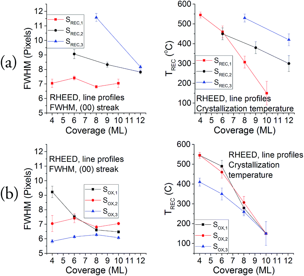 | ||
| Fig. 5 FWHM of the (00) streak and streaks appearance temperature for (a) SREC and (b) SOX samples. | ||
The morphological properties and thickness of the STO samples were explored with AFM and XRR. AFM images for samples SREC,1 and SOX,3 are shown in Fig. 6a as an example, since all samples show a similar planar morphology. Some small particles can be seen in some samples, with heights ranging from 3 to 4 nm, and widths from 50 to 110 nm: they could be attributed to small particulates from the STO deposition, or even contamination (the AFM images are performed ex situ on air). No signs of the original steps of the Si(001) substrate32 are seen in them, which can be attributed to the resolution of the AFM microscope used. The RMS values found for SREC and SOX samples (Fig. 6b) range from 0.2 to 0.45 nm, and no trend can be observed with the variation in the crystallization or oxidation coverage. It can be therefore concluded that the variation of these parameters have no impact on the morphology of the samples. The XRR fitting results (the fittings were already shown in Fig. 3) for the STO layer are shown in Table 4. The thickness of the samples are consistently around 3.1 nm, except for samples SREC,2 and SREC,,3 where 12 ML were deposited instead of 10. The densities are satisfactorily close to the nominal density of STO (5.11 g cm−3), except in the case of sample SPR,2 where the fittings yield a value of 3.66 ± 0.08 g cm−3. This smaller value is an indication that the second crystallization procedure, while it minimizes the interface reactions and increases its sharpness, does not supply enough energy to the STO layer to fully densify.
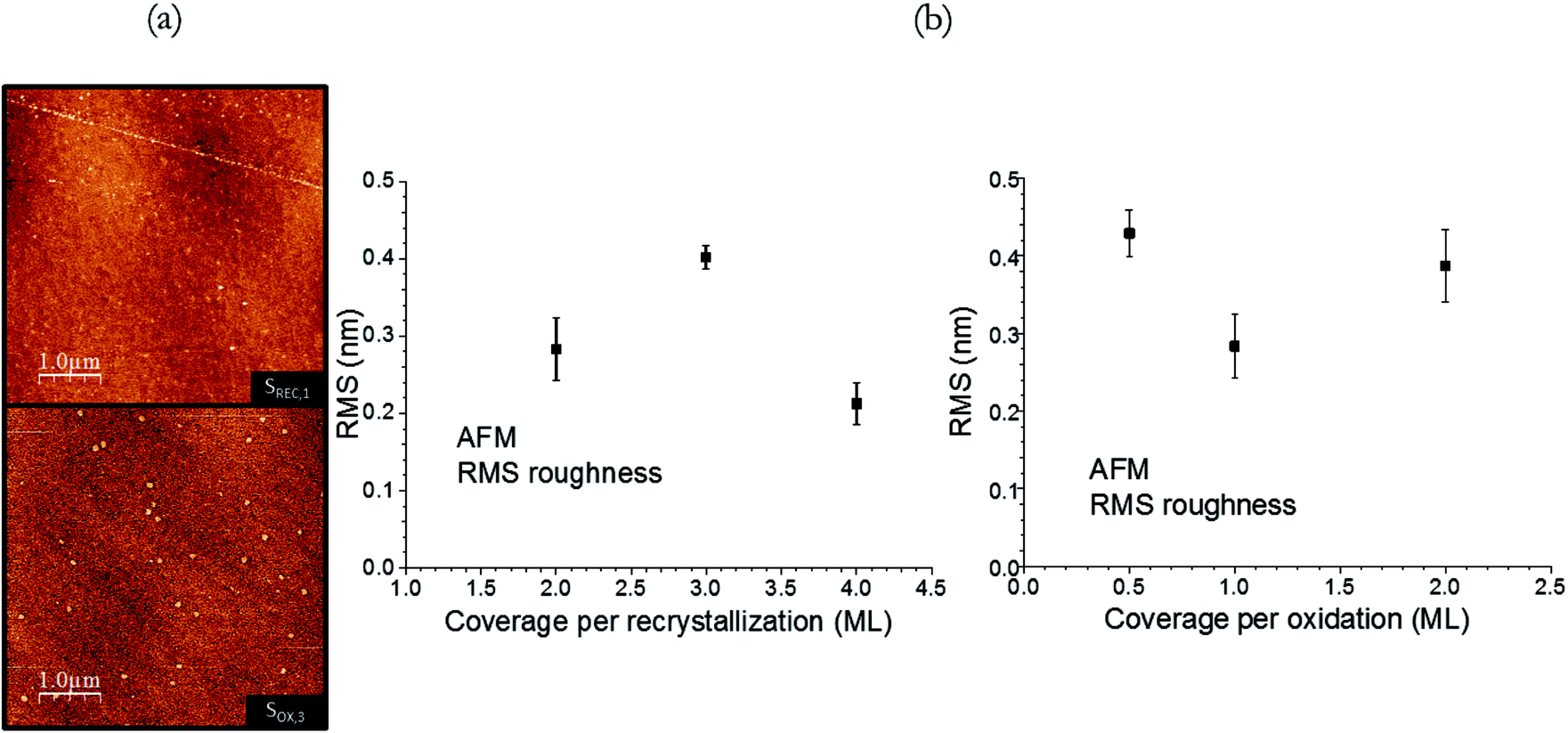 | ||
| Fig. 6 (a) AFM images for samples SREC,1 and SOX,3 (b) RMS values for SREC and SOX samples. | ||
| STO layer | ||
|---|---|---|
| Sample | Thickness (nm) | Density (g cm−3) |
| SREC,1 | 3.1 ± 0.2 | 5.1 ± 0.3 |
| SREC,2 | 3.3 ± 0.3 | 5.1 ± 0.4 |
| SREC,3 | 3.4 ± 0.1 | 4.9 ± 0.4 |
| SOX,1 | 3.1 ± 0.1 | 5.1 ± 0.1 |
| SOX,2 | 3.1 ± 0.2 | 5.1 ± 0.3 |
| SOX,3 | 3.1 ± 0.3 | 5.1 ± 0.5 |
| SPR,1 | 3.1 ± 0.3 | 5.1 ± 0.5 |
| SPR,2 | 3.1 ± 0.3 | 3.6 ± 0.5 |
The composition of the samples was assessed using XPS. Fig. 7 shows the XPS spectra for the Sr 3d, Ti 2p and O 1s regions, all taken at a 20° take-off angle. All the spectra show the expected STO contributions in these three regions (O 1s: 529.5 eV; Ti 2p3/2: 458.3 eV; Sr 3d5/2: 132.9 eV (ref. 33)). The O 1s region also shows an extra contribution at ∼531 eV, and a small shoulder at 533 eV: both of these contributions can be assigned to atmospheric contamination during the sample transport from the PLD to the XPS chamber.34 Fittings were performed in all spectra in order to assess these contributions: Fig. 8a shows them for sample SREC,1. Aside from the previously discussed STO peaks, an extra contribution appears in the Sr 3d (133.6 eV), which is attributed to surface SrCO3.35 The formation of SrCO3 at the surface is caused by the on-air sample transportation from the PLD chamber to the XPS equipment, and it's attributed to the reaction of the topmost Sr atoms of the STO surface with CO2. The composition of the STO layers was calculated using the STO contribution peaks, and the atomic sensitivity factors supplied by the spectrometer manufacturer were corrected by measuring a stoichiometric STO substrate cleaned in UHV conditions. Fig. 8b shows the results for all samples studied. All of them show atomic fractions close to the stoichiometric STO composition (60% O, 20% Sr and 20% Ti). Samples SREC,1 and SOX,3 show less differences in the Sr/Ti ratio than the rest, which correlates nicely with the improved surface crystallinity properties seen in Fig. 4. Meanwhile, SPR samples show almost no differences in their composition, which means that the crystallization procedure has an important effect in the density of the layer, but not on its composition.
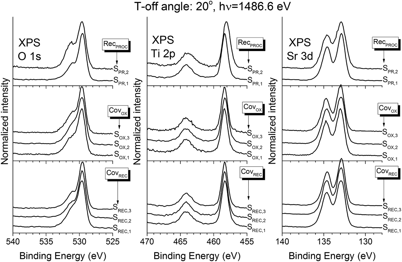 | ||
| Fig. 7 XPS spectra of the O 1s, Sr 3d and Ti 2p regions of all the samples, taken at a take-off angle of 20°. | ||
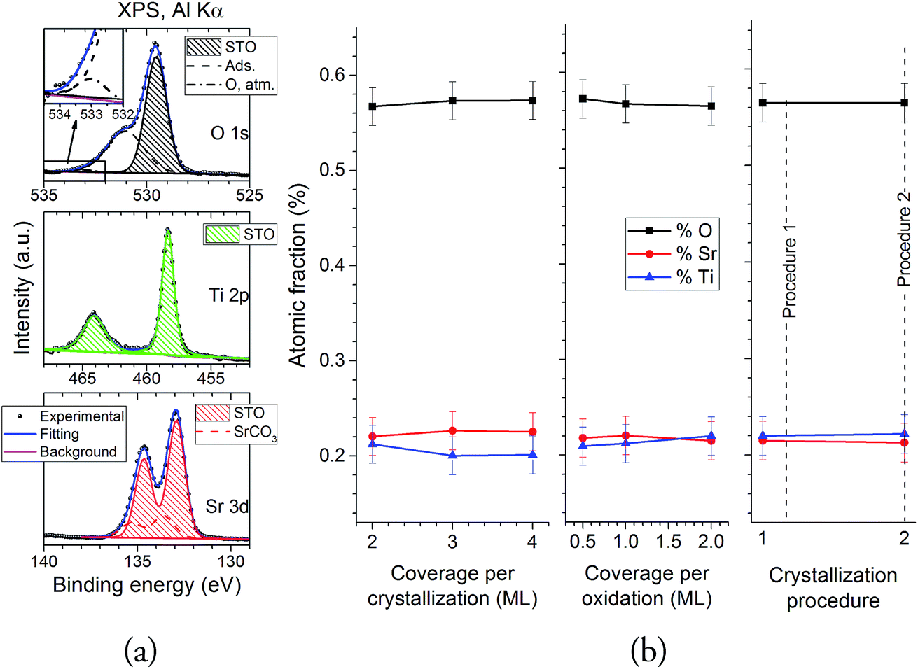 | ||
| Fig. 8 (a) Sample fittings for the O 1s, Ti 2p and Sr 3d spectra of sample SREC,1. (b) O, Sr and Ti atomic fractions for all the samples studied. | ||
All of these results indicate that the best combination for the growth of the highest quality STO samples is the deposition of 2 ML of amorphous STO, oxidation of these 2 ML, and crystallization of this oxidized 2 ML at a temperature of 545 °C for 15 min. They also show that decreasing the thermal budget leads to an interface sharpness improvement, but that decreasing it too much causes the STO layer to not be fully densified. These results can be explained as a result of the necessary balance between the minimization of the thermal budget, critical crystallization thickness, and sufficient coverage of the buffer layer. As it was clear from the XPS results of the interface, the thermal budget has to be minimized as much as possible in order to increase the interface sharpness, but the decrease in the density of sample SPR,2 means that a minimum amount of time and temperature needs to be applied to the sample in order to fully densify the STO layer. The results shown in this work suggests that a UHV heating of 545 °C for 15 min fulfills these two conditions satisfactorily. Meanwhile, the combination of 2 ML for the crystallization and oxidation stages can also be explained in the same terms. More coverage needs more energy to recrystallize, so this amount should be minimized as much as possible; but a certain amount of material should be deposited so the coverage is above the critical thickness. The results show that 2 ML is the best amount of amorphous STO in order to achieve this balance on the crystallization phase. Meanwhile, the amount of material before the oxidation stage must be as high as this coverage before the crystallization phase allows, so a full coverage of the Sr buffer layer is ensured, and possible reactions of bare buffer layer parts are minimized.
4 Conclusions
The impact of three key parameters (coverage per crystallization, coverage per oxidation and crystallization procedure) on the multi-staged growth of epitaxial ultra-thin STO layers on Si(001) by PLD has been explored using an array of in and ex situ techniques. The main results and conclusions can be summarized as follows:(1) The minimization of the thermal budget during the crystallization phase increases the interface sharpness, although a certain energy has to be supplied to the system in order to ensure an adequate density of the STO layer.
(2) A coverage of 2 ML before every crystallization phase yields the best results in terms of crystallization starting temperature, surface crystalline quality and stoichiometry.
(3) The optimal coverage at the oxidation phase must be the highest that the crystallization phase coverage allows (2 ML).
These results are explained in terms of the necessary balance between critical thickness and crystallization energy minimization, and the need to ensure enough STO coverage of the buffer layer so any possible reactions during the oxidation phase are discarded. Overall, they showcase that PLD is a powerful and more versatile technique than MBE, and that proper optimization of all growth parameters lead to ultra-thin oxide samples with properties comparable to those obtained by using MBE. In addition, these results represent an important step towards the goal of creating high-quality STO templates with PLD, improving the general knowledge about the physics behind oxide/silicon interfaces grown by this technique, and allowing us to further explore novel ways for the integration of complex oxides on silicon technologies.
Acknowledgements
This research has been funded by the ENPIEZO international project (M-ERA.NET 3330-14-500197) and by the National project “Growth of high quality piezoelectric thin films on silicon using pulsed laser deposition” (code number: J2-6759). The authors would like to express their gratitude to Urška Gabor (Advanced Materials department, Jožef Stefan Institute, Ljubljana, Slovenia) and Tatjana Filipič (Department of Surface Engineering and Optoelectronics, Jožef Stefan Institute, Ljubljana, Slovenia) for their invaluable help and assistance in the sample growth and XPS measurements, respectively.References
- R. A. McKee, F. J. Walker and M. F. Chisholm, Phys. Rev. Lett., 1998, 81, 3014–3017 CrossRef CAS.
- Z. Yu, J. Ramdani, J. A. Curless, C. D. Overgaard, J. M. Finder, R. Droopad, K. W. Eisenbeiser, J. A. Hallmark, W. J. Ooms and V. S. Kaushik, J. Vac. Sci. Technol., B: Microelectron. Nanometer Struct.--Process., Meas., Phenom., 2000, 18, 2139–2145 CrossRef CAS.
- Z. Jovanović, M. Spreitzer, J. Kovac, D. Klement and D. Suvorov, ACS Appl. Mater. Interfaces, 2014, 6, 18205–18214 Search PubMed.
- Z. Jovanović, M. Spreitzer, U. Gabor and D. Suvorov, RSC Adv., 2016, 6, 82150–82156 RSC.
- W. Kern and D. Puotinen, RCA Rev., 1970, 31, 187–206 CAS.
- M. Spreitzer, R. Egoavil, J. Verbeeck, D. H. Blank and G. Rijnders, J. Mater. Chem. C, 2013, 1, 5216–5222 RSC.
- T. Takahagi, I. Nagai, A. Ishitani, H. Kuroda and Y. Nagasawa, J. Appl. Phys., 1988, 64, 3516–3521 CrossRef CAS.
- D. Klement, M. Spreitzer and D. Suvorov, Appl. Phys. Lett., 2015, 106, 071602 CrossRef.
- B. K. Moon and H. Ishiwara, Jpn. J. Appl. Phys., Part 1, 1994, 33, 1472 CrossRef CAS.
- G. Z. Liu, Q. Y. Lei and X. X. Xi, Appl. Phys. Lett., 2012, 100, 202902 CrossRef.
- C.-H. Liu, X. Zhen Liu and Y. Fu, Trans. Mater. Heat Treat., 2007, 2, 26–29 Search PubMed.
- F. Hanzig, J. Hanzig, E. Mehner, C. Richter, J. Veselý, H. Stöcker, B. Abendroth, M. Motylenko, V. Klemm, D. Novikov and D. C. Meyer, J. Appl. Crystallogr., 2015, 48, 393–400 CrossRef CAS PubMed.
- A. Imanaka, T. Sasaki, Y. Hotta and S. Ichi Satoh, Extended Abstracts of the 2013 International Conference on Solid State Devices and Materials, Fukuoka, 2013, pp. 274–275 Search PubMed.
- F. Sánchez, C. Ocal and J. Fontcuberta, Chem. Soc. Rev., 2014, 43, 2272–2285 RSC.
- S.-B. Mi, C.-L. Jia, V. Vaithyanathan, L. Houben, J. Schubert, D. G. Schlom and K. Urban, Appl. Phys. Lett., 2008, 93, 101913 CrossRef.
- W. Press, S. Teukolsky, W. Vetterling and B. Flannery, Numerical Recipes in C++: The Art of Scientific Computing, Cambridge University Press, 2002, p. 699 Search PubMed.
- S. Tanuma, C. J. Powell and D. R. Penn, Surf. Interface Anal., 2011, 43, 689–713 CrossRef CAS.
- I. Horcas, R. Fernández, J. M. Gómez-Rodríguez, J. Colchero, J. Gómez-Herrero and A. M. Baro, Rev. Sci. Instrum., 2007, 78, 013705 CrossRef CAS PubMed.
- D. Klement, Ph.D. thesis, Mednarona Podiplomska Šola Jožefa Stefana, 2015.
- L. Goncharova, D. Starodub, E. Garfunkel, T. Gustafsson, V. Vaithyanathan, J. Lettieri and D. Schlom, J. Appl. Phys., 2006, 100, 014912 CrossRef.
- G. Saint-Girons, R. Bachelet, R. Moalla, B. Meunier, L. Louahadj, B. Canut, A. Carretero-Genevrier, J. Gazquez, P. Regreny and C. Botella, et al., Chem. Mater., 2016, 28, 5347–5355 CrossRef CAS.
- R. Pérez-Casero, J. Perrière, A. Gutiérrez-Llorente, D. Defourneau, E. Millon, W. Seiler and L. Soriano, Phys. Rev. B: Condens. Matter Mater. Phys., 2007, 75, 165317 CrossRef.
- P. Ahmet, T. Koida, M. Yoshimoto, H. Koinuma and T. Chikyow, MRS Proceedings, 2001, 700, S3.4 CrossRef.
- J. W. Park, S. H. Baek, C. W. Bark, M. D. Biegalski and C. B. Eom, Appl. Phys. Lett., 2009, 95, 061902 CrossRef.
- X. Y. Zhou, J. Miao, X. B. Lu, P. F. Lee, J. Y. Dai, H. L. W. Chan, C. L. Choy and Y. Wang, Integr. Ferroelectr., 2006, 86, 109–116 CrossRef.
- R. Z. Bakhtizin, J. Kishimoto, T. Hashizume and T. Sakurai, J. Vac. Sci. Technol., B: Microelectron. Nanometer Struct.--Process., Meas., Phenom., 1996, 14, 1000–1004 CrossRef CAS.
- L. Ji, M. D. McDaniel, S. Wang, A. B. Posadas, X. Li, H. Huang, J. C. Lee, A. A. Demkov, A. J. Bard and J. G. Ekerdt, et al., Nat. Nanotechnol., 2015, 10, 84–90 CrossRef CAS PubMed.
- A. Thøgersen, J. H. Selj and E. S. Marstein, J. Electrochem. Soc., 2012, 159, D276–D281 CrossRef.
- I. McColm, Dictionary of Ceramic Science and Engineering, Springer, Netherlands, 2013 Search PubMed.
- G. Niu, G. Saint-Girons, B. Vilquin, G. Delhaye, J.-L. Maurice, C. Botella, Y. Robach and G. Hollinger, Appl. Phys. Lett., 2009, 95, 062902 CrossRef.
- M. Choi, A. Posadas, R. Dargis, C.-K. Shih, A. A. Demkov, D. H. Triyoso, N. David Theodore, C. Dubourdieu, J. Bruley and J. Jordan-Sweet, J. Appl. Phys., 2012, 111, 064112 CrossRef.
- R. G. Dixson, N. G. Orji, J. Fu, V. Tsai, E. D. Williams, R. Kacker, T. V. Vorburger, H. L. Edwards, D. Cook and P. E. West, et al., 26th Annual International Symposium on Microlithography, 2001, pp. 157–168 Search PubMed.
- R. P. Vasquez, Surf. Sci. Spectra, 1992, 1, 129–135 CrossRef CAS.
- F. Amy, A. Wan, A. Kahn, F. J. Walker and R. A. McKee, J. Appl. Phys., 2004, 96, 1601–1606 CrossRef CAS.
- F. Hanzig, J. Hanzig, E. Mehner, C. Richter, J. Veselý, H. Stöcker, B. Abendroth, M. Motylenko, V. Klemm, D. Novikov and D. C. Meyer, J. Appl. Crystallogr., 2015, 48, 393–400 CrossRef CAS PubMed.
| This journal is © The Royal Society of Chemistry 2017 |