
 Open Access Article
 This Open Access Article is licensed under a Creative Commons Attribution-Non Commercial 3.0 Unported Licence
Non-equilibrium synthesis and characterization of n-type Bi2Te2.7Se0.3 thermoelectric material prepared by rapid laser melting and solidification†
Yu Maoa,
Yonggao Yan*a,
Keping Wua,
Hongyao Xiea,
Zekun Xiua,
Jihui Yang b,
Qingjie Zhanga,
Ctirad Uherc and
Xinfeng Tang*a
b,
Qingjie Zhanga,
Ctirad Uherc and
Xinfeng Tang*a
aState Key Laboratory of Advanced Technology for Materials Synthesis and Processing, Wuhan University of Technology, Wuhan, Hubei 430070, China. E-mail: yanyonggao@whut.edu.cn; tangxf@whut.edu.cn
bDepartment of Materials Science and Engineering, University of Washington, Seattle, Washington 98195, USA
cDepartment of Physics, University of Michigan, Ann Arbor, Michigan 48109, USA
First published on 18th April 2017
Abstract
Commercial production of thermoelectric (TE) modules features energy-intensive and time-consuming processes. Here, we propose a rapid, facile and low cost fabrication process for n-type single phase Bi2Te2.7Se0.3 that combines self-propagating high-temperature synthesis (SHS) with the laser non-equilibrium 3D printing method based on selective laser melting (SLM). The optimal SLM processing window for high quality single layers has been determined. Results show that the chemical composition of the sample is very sensitive to the laser energy density (EV) due to the selective vaporization of Se and Te. For energy densities EV of less than 33.3 J mm−3, the composition of the SLM-processed samples is relatively stable. However, as EV exceeds 33.3 J mm−3 and increases further, the vaporization rate of Te and Se significantly increases and is much higher than that of Bi. Empirical formulae relating the chemical composition of the resulting materials with the values of EV are obtained and are used to predict the composition of the SLM-processed material. Most importantly, the temperature dependent TE properties of the SLM-fabricated bulk sample result in a maximum ZT value of 0.84 at 400 K, which is comparable to that of the commercially available material. The work has laid a foundation for the future utilization of this technique for the fabrication of Bi2Te3-based thermoelectric modules.
Introduction
TE technology realizes the direct conversion of heat into electricity via the Seebeck effect and heat pumping via the Peltier effect.1,2 Compared with other energy conversion technologies, TE conversion has advantages of no moving parts, long life, exceptional reliability, noise-free operation and no pollution of the environment.3,4 Bi2Te3-based solid solutions possess the best TE performance near room temperature and have been extensively used in the commercial TE applications, such as power generation and refrigeration.5–8 The usual fabrication route of commercial bulk thermoelectric modules based on Bi2Te3 includes zone melting (ZM) of ingots followed by a series of processes, such as slicing, plating, cleaning and soldering. The process is generally time-consuming with considerable material loss and has a high cost, especially when manufacturing micro TE devices.9,10 Therefore, it is of great significance to develop new preparation methods, which are simple, require low energy consumption and preserve a high raw material utilization rate.Unlike the traditional manufacturing methods, selective laser melting (SLM) is an example of the additive manufacturing technology, in which a thin layer of powder is melted using a laser beam and subsequently rapidly solidifies. In this way, 3D objects of full density and virtually any shape can be built by successive steps of powder deposition followed by laser-induced melting.11–13 The SLM process features rapid heating and cooling rates during the non-equilibrium laser processing and as such, the technique is able to produce materials with fine nanostructures. Moreover, the raw materials are utilized more efficiently and there is no need for post-processing. With the above advantages, SLM has been widely employed in the manufacture of metallic parts for the aerospace and automobile industries.12,14–16 If one could use SLM in the parallel production of p- and n-type TE legs, as well as in rapid joining of TE legs to electrodes and insulating substrates, the fabrication of TE modules would be carried out in just one integrated step with much improved efficiency and reduced cost. The key element in the SLM-based technique of TE module manufacturing is the fabrication of TE legs with good control over their chemical composition, phase, microstructure and TE performance.
The SLM technique has been successfully used in the preparation of structural materials, mostly metals and alloys, which have rather high melting points.16–19 Moreover, physical properties of structural materials are mainly affected by the microstructure and the forming quality. In contrast, thermoelectric materials are semiconductors that usually possess a lower melting point, lower thermal conductivity, poor ductility and weak thermal shock resistance. All of the above are likely to contribute to the formation of macro and micro defects during SLM processing of semiconductors. Even more important, since the properties of TE materials are more sensitive to their chemical composition, phase structure and microstructure, it is a considerable challenge to obtain p/n TE legs of desirable composition, free of defects and with high TE performance via the laser non-equilibrium technique. Indeed, there are very few reports in the literature employing the SLM technique in the preparation of thermoelectric materials. In 2016, El-Desouky et al.20,21 tried to process Bi2Te3 by the SLM technique, and explored the effect of various processing parameters on the depth of the molten pool and on the resulting microstructure. However, the chemical composition and thermoelectric properties of their SLM-processed samples were not studied. As the TE properties of Bi2Te3-based materials are very sensitive to their chemical composition, it is of vital importance to assess changes in the chemical composition arising during the SLM process. For example, a slight change in the ratio of Te to Se in n-type Bi2Te3−xSex can greatly affect the final electronic properties of the material.22–24
In this study, n-type Bi2Te2.7Se0.3 powder, prepared by the ultra-fast and low-cost self-propagating high-temperature synthesis (SHS),25 was used in SLM experiments. The influence of the laser volumetric energy density on the macroscopic defects, chemical composition, phase structure and thermoelectric properties was systematically studied. As a result, the optimal processing parameters have been determined. In addition, we have proposed empirical formulas to predict and achieve the precise control over the actual composition of samples following the SLM process. Based on these formulas, the content of Te in the raw material has been modified to fabricate SLM samples having a similar composition and comparable TE performance to n-type Bi2Te3-based materials prepared by the traditional synthesis routes. The work demonstrates the viability of SLM as a rapid fabrication technique of TE materials and perhaps even future TE modules.
Experimental
High purity powders of Bi (99.99%, 200 mesh), Te (99.999%, 200 mesh) and Se (99.999%, 200 mesh) were used to synthesize the Bi2Te2.7Se0.3 compound by SHS. Details concerning the SHS process can be found elsewhere.24 The SHS-prepared ingot was ground into powder (300 mesh) by a planetary ball mill (300 rpm for 6 h). The morphology and size distribution of the powder are shown in Fig. 1, which documents that the average particle size is 3.4 μm. A small part of the powder was sintered by spark plasma sintering (SPS) to obtain substrates of 20 mm in diameter and 3 mm thickness for subsequent SLM experiments. The rest of the powder was mixed with alcohol (a solid content of 17 vol%) to obtain a slurry, which was then spread on the substrate by a scraper. A commercial fiber laser (MFSC-100W) was used for SLM processing. The maximum output power, wavelength and spot size of the laser were 100 W, 1064 nm and 100 μm, respectively. All experiments were carried out under high-purity argon of 0.5 atm.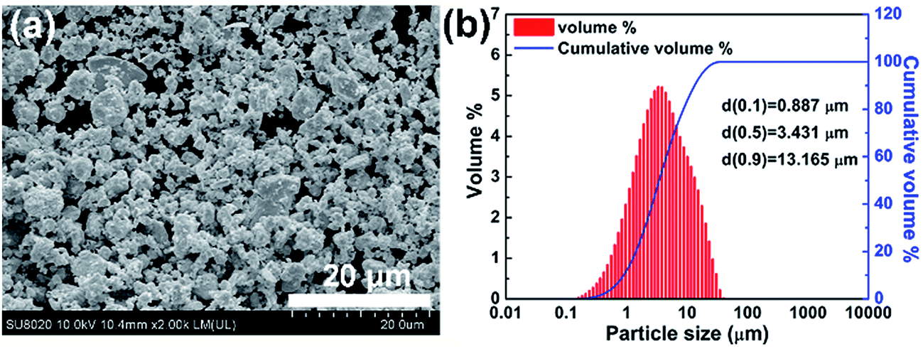 | ||
| Fig. 1 (a) SEM image and (b) particle size distribution for the SHS-prepared Bi2Te2.7Se0.3 powder used for SLM. | ||
The particle size was measured by a laser diffraction technique (Marlven, Mastersizer 2000). The surface morphology and microstructure of the samples were characterized by field emission scanning electron microscopy (Hitachi FESEM, SU8020). The phase identification was performed by an X-ray diffraction (PANalytical Empyrean) apparatus operating with a Cu Kα radiation at 40 kV and 40 mA. The actual chemical composition of samples was analyzed by electron probe micro-analysis (JEOL EPMA, JXA-8230). The spatially resolved Seebeck coefficient was measured by a potential-Seebeck-microprobe instrument (Panco PSM) with a spatial resolution of 20 μm. The temperature dependent electrical conductivity (σ) and Seebeck coefficient (α) for SLM bulk samples were measured simultaneously using commercial equipment (ZEM-3, Ulvac Riko, Inc.) under a low pressure He atmosphere in the temperature range of 300–550 K. The thermal conductivity (κ) of the SLM bulk samples was calculated from the relationship κ = DCpd, where D is the thermal diffusivity obtained by the laser flash method (LFA-457, Netzch, German), Cp is the specific heat measured by a differential scanning calorimeter (DSC Q20, TA Instrument, USA), and d is the density measured by the Archimedes method. The Hall coefficient (RH) at room temperature was determined by a Physical Properties Measurements System (PPMS-9, Quantum Design, USA) with the magnetic field of 1 T. The corresponding carrier concentration (n) and carrier mobility (μH) were calculated by the following equations: n = 1/eRH and μH = σRH.
Results and discussion
Processing window
Fig. 2 shows the influence of the SLM process parameters on the forming quality of a single layer. Laser volumetric energy density EV is being used to quantify the effect of laser energy impinging on a layer of powder and is defined as26
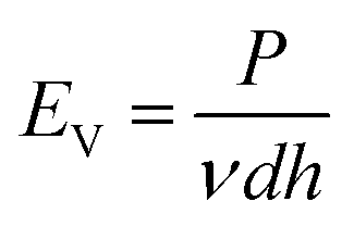 | (1) |
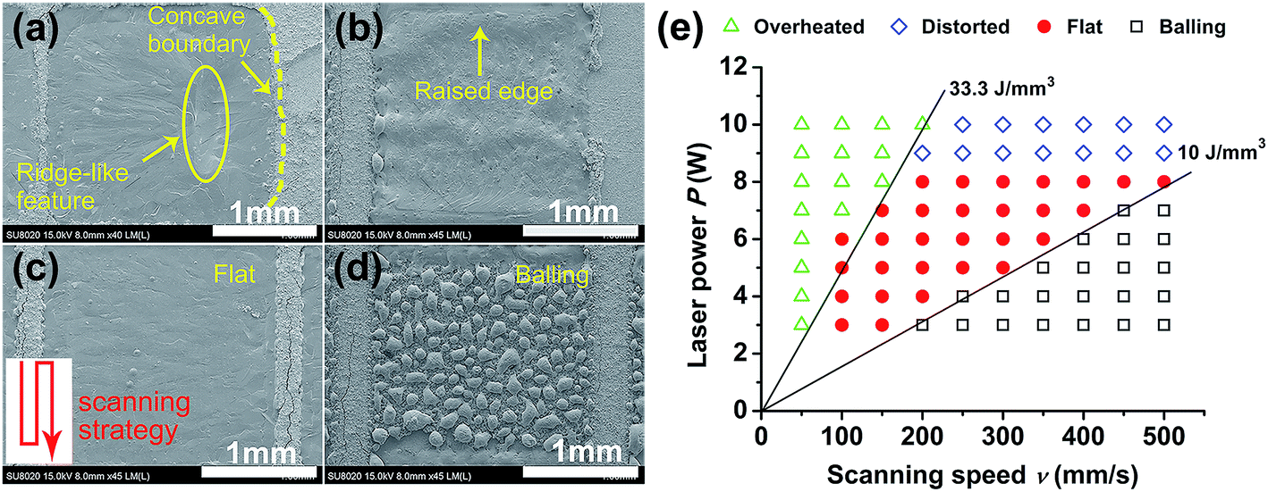 | ||
| Fig. 2 SEM images of four typical surface morphologies of SLM-prepared layers: (a) overheated; (b) distorted; (c) flat; and (d) balling. (e) Processing map for the first layer of Bi2Te2.7Se0.3. | ||
Fig. 2(a)–(d) show four typical morphologies (overheated, distorted, flat and balling) of the single layers (2 × 2 mm2) obtained under different laser power (P = 3–10 W) and scanning speed (ν = 50–500 mm s−1). Meanwhile, the hatch spacing and powder layer thickness were set at 0.05 mm and 0.03 mm, respectively. The scanning strategy is sketched with a red line in Fig. 2(c).
Based on the above four typical morphologies, the processing parameters can be divided into four groups delineated in Fig. 2(e). At high laser powers (P > 8 W) and low scanning speeds (ν < 200 mm s−1), resulting in EV > 33.3 J mm−3, the boundary region between the processed and unprocessed layer of powder develops a distinct concave profile, as shown in Fig. 2(a). When such a high EV is applied, the temperature of the molten pool increases and the heat-affected zone is large. Eventually, the powder outside the laser irradiated region also melts and the concave boundary forms. At the same time, the viscosity of the melt decreases with the increasing molten pool temperature, leading to an increasing liquid flow rate driven by Marangoni effect.27 Therefore, a ridge-like feature forms inside the layer.
When the same laser power (P > 8 W) is coupled with a high scanning speed (ν > 200 mm s−1), EV decreases to around 10–33.3 J mm−3, and the concave boundary layer disappears. However, a raised edge is found at both ends of the laser scanning path, which is mainly due to the fact that the actual scanning speed at the start and end points of the laser path is much lower than the speed over the central region. Consequently, the laser beam has interacted with the powder for a longer time at both ends of the path, the temperature of the molten pool has increased, giving rise to raised edges at both ends, as shown in Fig. 2(b). This phenomenon becomes more pronounced when the scanning speed is higher.
Fig. 2(c) shows a layer with a flat surface finish obtained when the laser power decreased to P ≤ 8 W yet EV was maintained in the range 10–33.3 J mm−3. In this case, the boundary becomes straight with no ridge-like feature observed on the surface. This demonstrates that the laser power is the dominant factor in determining the quality of each layer.
When the laser power is so low or the scanning speed is so high that the energy density falls below 10 J mm−3, the laser beam is unable to melt the powder bed completely. Lower temperature of the melt and its higher viscosity results in a large wetting angle between the molten pool and the substrate and, eventually, it gives rise to balling,28 as seen in Fig. 2(d).
The above results imply that, in order to obtain a high quality n-type Bi2Te3 material, the laser power should be below 8 W, while EV should be controlled between 10 and 33.3 J mm−3. Of course, as the powder layer thickness is altered, the optimal processing window also changes. Nevertheless, the optimal processing window obtained here serves as a good starting point for further optimization to ensure successful fabrication of Bi2Te3-based thermoelectric materials.
Chemical composition
For TE materials, it is also essential to consider changes in the chemical composition that might take place during the SLM process, and that might directly influence the TE performance. To shed the light on this issue, we studied what effect a variation of the laser energy density EV set above 10 J mm−3 (the level above the region where balling dominates) has on the chemical composition of the resulting material. Table 1 lists the SLM processing parameters and the actual chemical composition of the processed samples. From the data it follows that relative contents of Se and Te in the SLM samples are both reduced compared to the raw powder (Bi2Te2.7Se0.3). Moreover, the loss of Te and Se increases sharply with the increasing EV.| Sample | EV (J mm−3) | P (W) | ν (mm s−1) | D (mm) | H (mm) | Actual composition |
|---|---|---|---|---|---|---|
| 1 | 12.5 | 6 | 200 | 0.08 | 0.03 | Bi2Te2.60Se0.23 |
| 2 | 20.0 | 6 | 200 | 0.05 | 0.03 | Bi2Te2.49Se0.20 |
| 3 | 26.7 | 4 | 100 | 0.05 | 0.03 | Bi2Te2.44Se0.22 |
| 4 | 33.3 | 6 | 200 | 0.03 | 0.03 | Bi2Te2.42Se0.21 |
| 5 | 40.0 | 6 | 100 | 0.05 | 0.03 | Bi2Te2.24Se0.18 |
| 6 | 44.4 | 8 | 200 | 0.03 | 0.03 | Bi2Te2.27Se0.19 |
| 7 | 53.3 | 4 | 50 | 0.05 | 0.03 | Bi2Te2.04Se0.16 |
| 8 | 66.7 | 6 | 100 | 0.03 | 0.03 | Bi2Te1.98Se0.11 |
| 9 | 80.0 | 6 | 50 | 0.05 | 0.03 | Bi2Te2.05Se0.11 |
| 10 | 88.9 | 8 | 100 | 0.03 | 0.03 | Bi2Te1.99Se0.10 |
Based on the Langmuir formula,29 the vaporization rate Ji (g cm−2 s−1) of element i in a molten pool of an alloy can be calculated as
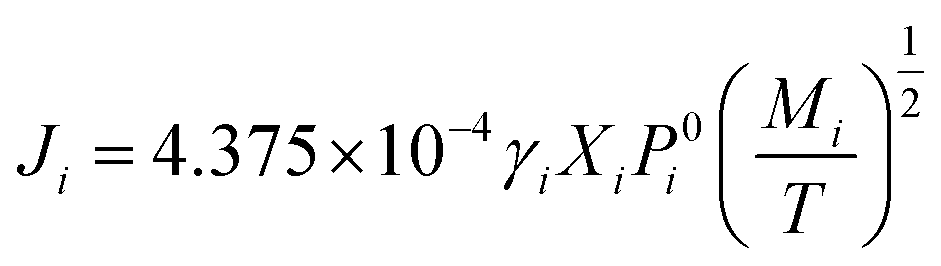 | (2) |
 | (3) |
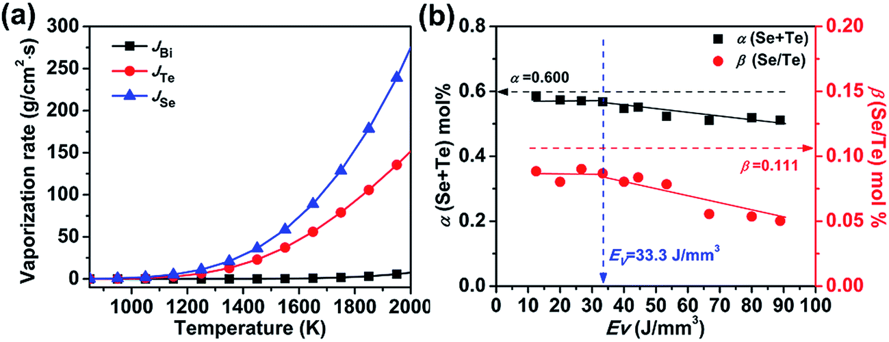 | ||
| Fig. 3 (a) Calculated vaporization rates of Se, Te and Bi; (b) dependence of parameters α and β dependence on the laser energy density EV. | ||
Since the vaporization rate of Bi during the SLM process is relatively low, we have chosen the combined total molar ratio of Te and Se in Bi2Te2.7Se0.3 (designated as α) and the relative molar ratio of Se with respect to Te (designated as β) to characterize the chemical composition of each sample. Fig. 3(b) shows the dependence of α and β on EV, where the black and red dashed lines show α (0.6) and β (0.111) of the raw powder, while the blue dashed line is located at EV = 33.3 J mm−3. The results suggest that both α and β of the SLM samples are significantly lower than those of the raw powder due to preferential vaporization of Se and Te during the SLM process. In fact, the data suggest that the loss of Se is more serious than the loss of Te, consistent with the higher vapor pressure of Se compared to Te. When EV is less than 33.3 J mm−3, α and β show little fluctuation because the molten pool's temperature is low under such a low energy density, and the vaporization rate is, consequently, also low. As EV increases above 33.3 J mm−3, α and β decrease rapidly, corresponding to an enhanced vaporization of Se and Te. A linear fit to the data in Fig. 3(b) yields empirical formulas for α and β with EV in the range of EV > 33.3 J mm−3:
| α = −0.00113EV + 0.600 | (4) |
| β = −0.000712EV + 0.111 | (5) |
Microstructure and phase composition
Fig. 4 shows SEM images of pores and their distribution that form in the SLM samples processed under different EV. At low EV = 20 J mm−3, there are no pores present on the polished surface. A few micro pores appear when the laser energy density EV is 40 J mm−3. As EV increases, the pores become gradually larger and their density increases. This is clearly evident in Fig. 4(c) and (d) where EV has reached values of 66.7 and 80 J mm−3, respectively. The density of pores has now increased markedly and their diameter is mostly in the range of 10 to 50 μm. The presence of the pores coincides with the much enhanced rates of vaporization of Se and Te observed at these high laser energy densities EV.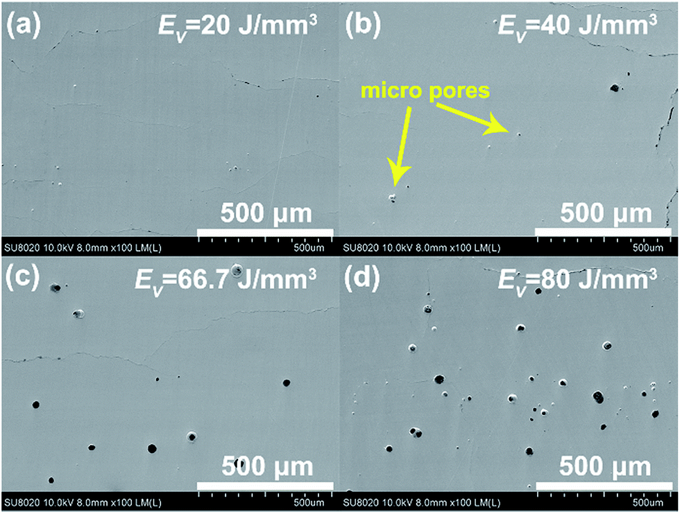 | ||
| Fig. 4 SEM images showing size and distribution of pores on polished SLM samples under different energy densities EV. | ||
Fig. 5 shows XRD patterns obtained on the SLM-processed layers at different EV. At low applied EV of 20 J mm−3, a single phase Bi2Te3 is obtained. However, as the laser energy density increases to 40 J mm−3, a second phase with composition Bi4Te5 appears. As EV increases to 66.7 J mm−3 and 80 J mm−3, the vaporization rate increases sharply and α is reduced to 0.53 and 0.51, respectively, resulting in the formation of BiTe. One can conclude that the enhanced vaporization of Se and Te leads to significant deviations in the stoichiometric ratio, which, in turn, brings about the formation of secondary phases and phase segregation. Therefore, as long as the form quality is acceptable, one should try to use the lowest possible laser energy density EV to avoid excessive losses of anion elements.
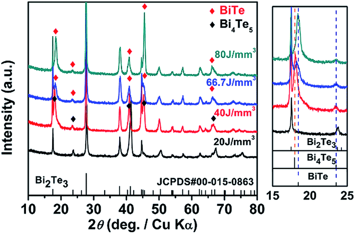 | ||
| Fig. 5 XRD patterns of SLM samples prepared with different energy densities. | ||
Transport properties
Based on the data in Fig. 3(b), some vaporization of Te and Se takes place even under the lowest laser energy density. In order to maintain the chemical composition of the SLM samples close to the traditionally desired n-type Bi2Te2.7Se0.3, it is necessary to adjust the composition of the starting raw material to compensate for the loss of Te and Se. Fig. 6 shows the XRD pattern and the Seebeck coefficient of the SLM sample containing a 10 mol% excess of Te in the starting powder prior to SHS and processed with the laser energy density EV of 20 J mm−3 (P = 6 W, ν = 200 mm s−1, d = 0.05 mm, h = 0.03 mm). As Fig. 6(a) attests to, the sample shows good phase purity. The actual composition after SLM is Bi2Te2.94Se0.09, i.e., α = 0.6024 and close to the nominal 0.6, indicating that excellent control of the composition in the SLM process can be achieved via carefully manipulating the processing parameters combined with an adjustment of the starting composition. The SLM-processed sample was subsequently annealed at 673 K for 24 h to eliminate residual stress and compositional inhomogeneity, if any. Fig. 6(b) presents average values of the Seebeck coefficient measured at room temperature. While the magnitude of the Seebeck coefficient of about 155 μV K−1 obtained on the SLM-processed sample is slightly lower than the Seebeck coefficient of zone-melted (ZM) samples,23 it is significantly superior to samples fabricated by the self-propagating high-temperature synthesis followed by spark plasma sintering (SHS-SPS)24 and to samples synthesized by melt spinning followed by spark plasma sintering (MS-SPS).31 Fig. 6(c) and (d) show the Seebeck coefficient distribution measured on the layer surface. The distribution of the Seebeck coefficients is reasonably homogeneous with the values falling between −145 μV K−1 and -165 μV K−1, with a standard deviation of 5.29 μV K−1. This confirms that the chemical composition is substantially uniform in the SLM sample.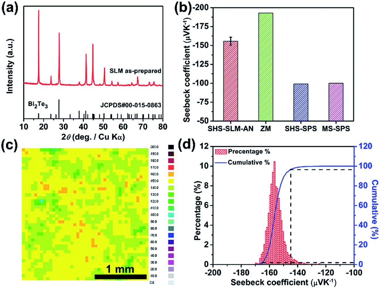 | ||
| Fig. 6 (a) XRD pattern of Te-compensated n-type SLM sample. (b) Average Seebeck coefficient of nominal Bi2Te2.7Se0.3 samples prepared by various techniques. (c and d) Spatially resolved Seebeck coefficient at room temperature. | ||
The Te-compensated n-type Bi2Te2.7Se0.3 bulk sample of 1.5 mm thickness was fabricated by stacking 60 layers on top of each other. The bulk sample shows a 97% relative density and is shown in Fig. S1 of the ESI.† The carrier concentration calculated from the measured RH of this sample is 3.18 × 1019 cm−3 with the Hall mobility of 154 cm2 V−1 s−1, both values very close to those of the SHS-prepared samples.24 Fig. 7(a)–(d) show the temperature dependent TE transport properties of the SLM bulk sample after annealing at 673 K for 36 h. Properties of the SHS-prepared Bi2Te2.85Se0.15 sample and of the ZM Bi2Te2.79Se0.21 sample24 are shown for comparison. Compared to the ZM sample, the SLM bulk sample shows modest electronic properties but a lower thermal conductivity at high temperatures due to limited intrinsic excitation.
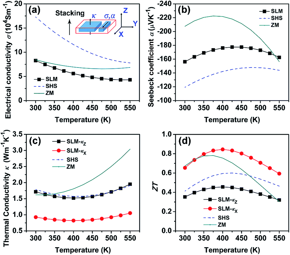 | ||
| Fig. 7 Temperature dependence of thermoelectric properties of SLM-prepared bulk sample: (a) electrical conductivity, (b) Seebeck coefficient, (c) thermal conductivity, and (d) ZT. The SHS and ZM data are from (ref. 24). | ||
It is important to note that, the thermal conductivity of the SLM bulk sample was measured parallel to the stacking direction z, while the electrical conductivity was measured in the xy plane (σxy), perpendicular to the stacking direction, as depicted in Fig. 7. The thermal and electrical conductivity along the same direction could not be obtained for the time being due to the limited thickness of samples our customized SLM apparatus can handle. However, by using a relationship curve proposed by Shen et al.,32 the thermal conductivity in the xy plane (κx) could be deduced from the measured thermal conductivity (κz) and the orientation factor F of (00l) diffractions observed on the SLM bulk sample. The XRD pattern (Fig. S2†) collected from the xy plane of the SLM bulk sample shows strong texture along the (110) direction, while the XRD pattern collected from the xz plane shows strong texture along the (00l) direction. Therefore, the measured thermal conductivity κz is almost along the ab plane of Bi2Te3, which is about two times higher than κx along the c axis.32 The calculated ZT value (solid black square in Fig. 7(d)) using κz and σxy thus greatly underestimates the TE performance of our sample. The F value is calculated to be 0.79, approaching the value of ZM Bi2Te3 (F = 1). This highly textured structure is confirmed by the SEM photos (Fig. S3†) of the cross section of the SLM bulk. According to Shen's relationship curve,32 κx/κz = 0.54. κx and ZT for the SLM bulk sample is then calculated and shown in Fig. 7(c) and (d), respectively. The calculated ZT using κx shows a maximum value of 0.84 at 400 K and is higher than the ZT values of the ZM and SHS-prepared samples in the whole temperature range measured. To sum up, the SLM bulk sample exhibits comparable, if not superior, TE performance compared to bulk samples prepared by the traditionally synthesis routes, such as ZM or SHS.24 Moreover, the content of Se in the SLM bulk sample could be adjusted to further optimize its ZT value.
These results demonstrate that the Bi2Te3-based material with a homogeneous composition and excellent TE performance can be prepared via the SLM technique under an appropriate control of the processing parameters and the starting composition.
Conclusions
In this work, n-type Bi2Te2.7Se0.3 thermoelectric material was prepared for the first time using a novel laser non-equilibrium heating technique. Results show that the laser energy density has a significant effect on the forming quality, stoichiometric ratio, microstructure, phase composition and thermoelectric properties. The optimal laser energy density for high formation quality Bi2Te2.7Se0.3 layers is in the range 10–33.3 J mm−3. Deviating significantly from this range results in balling (too low laser energy density) or vaporization of anion species (too high laser energy density). Some vaporization of Se and Te during the SLM process is unavoidable even at low laser energy density of less than 33.3 J mm−3, but its effect seems minimal as the single phase Bi2Te3 structure is maintained. However, secondary phases of Bi4Te5 and BiTe gradually form as the laser energy density exceeds 33.3 J mm−3 and the evaporation of Te and Se becomes a serious problem. By modifying the content of Te and Se in the starting raw material and selecting appropriate laser processing parameters, the composition of n-type Bi2Te2.7Se0.3 samples prepared by SLM can be controlled, resulting in a material with the maximum ZT value of 0.84 at 400 K, the value comparable to ZT values of zone-melted (ZM) samples. Our work demonstrates that the SLM process can be a promising synthesis route for fabrication of TE materials. With appropriate modifications, the techniques might even be used in the future fabrication of TE modules.Acknowledgements
We wish to acknowledge support from the National Basic Research Program of China (973 program) under project 2013CB632502, the Natural Science Foundation of China (Grant No. 51521001, 51401153) and the 111 project of China (Grant No. B07040).References
- T. M. Tritt and M. A. Subramanian, MRS Bull., 2006, 31, 188–194 CrossRef.
- L. E. Bell, Science, 2008, 321, 1457–1461 CrossRef CAS PubMed.
- Y. Zhang, M. Cleary, X. Wang, N. Kempf, L. Schoensee, J. Yang, G. Joshi and L. Meda, Energy Convers. Manage., 2015, 105, 946–950 CrossRef.
- Q. H. Zhang, X. Y. Huang, S. Q. Bai, X. Shi, C. Uher and L. D. Chen, Adv. Eng. Mater., 2016, 18, 194–213 CrossRef CAS.
- R. Venkatasubramanian, E. Siivola, T. Colpitts and B. O'Quinn, Nature, 2001, 413, 597–602 CrossRef CAS PubMed.
- M. A. Karri, E. F. Thacher and B. T. Helenbrook, Energy Convers. Manage., 2011, 52, 1596–1611 CrossRef CAS.
- L. W. da Silva and M. Kaviany, In. J. Heatd Mass Transfer, 2004, 47, 2417–2435 CrossRef CAS.
- W. Glatz, E. Schwyter, L. Durrer and C. Hierold, J. Microelectromech. Syst., 2009, 18, 763–772 CrossRef CAS.
- J. Jiang, L. Chen, S. Bai, Q. Yao and Q. Wang, J. Cryst. Growth, 2005, 277, 258–263 CrossRef CAS.
- W. Liu, Q. Jie, H. S. Kim and Z. Ren, Acta Mater., 2015, 87, 357–376 CrossRef CAS.
- J. P. Kruth, L. Froyen, J. Van Vaerenbergh, P. Mercelis, M. Rombouts and B. Lauwers, J. Mater. Process. Technol., 2004, 149, 616–622 CrossRef CAS.
- D. D. Gu, W. Meiners, K. Wissenbach and R. Poprawe, Int. Mater. Rev., 2013, 57, 133–164 CrossRef.
- E. C. Santos, M. Shiomi, K. Osakada and T. Laoui, Int. J. Mach. Tool Manufact., 2006, 46, 1459–1468 CrossRef.
- J. Dutta Majumdar and I. Manna, Int. Mater. Rev., 2013, 56, 341–388 CrossRef.
- E. Uhlmann, R. Kersting, T. B. Klein, M. F. Cruz and A. V. Borille, Procedia CIRP, 2015, 35, 55–60 CrossRef.
- Q. Shi, D. Gu, M. Xia, S. Cao and T. Rong, Opt. Laser Technol., 2016, 84, 9–22 CrossRef CAS.
- M. L. Montero Sistiaga, R. Mertens, B. Vrancken, X. Wang, B. Van Hooreweder, J.-P. Kruth and J. Van Humbeeck, J. Mater. Process. Technol., 2016, 238, 437–445 CrossRef CAS.
- J. Suryawanshi, K. G. Prashanth, S. Scudino, J. Eckert, O. Prakash and U. Ramamurty, Acta Mater., 2016, 115, 285–294 CrossRef CAS.
- Z. Sun, X. Tan, S. B. Tor and W. Y. Yeong, Mater. Des., 2016, 104, 197–204 CrossRef CAS.
- A. El-Desouky, M. Carter, M. A. Andre, P. M. Bardet and S. LeBlanc, Mater. Lett., 2016, 185, 598–602 CrossRef CAS.
- A. El-Desouky, M. Carter, M. Mahmoudi, A. Elwany and S. LeBlanc, J. Manuf. Process, 2017, 25, 411–417 CrossRef.
- J. Y. Yang, T. Aizawa, A. Yamamoto and T. Ohta, J. Alloys Compd., 2000, 312, 326–330 CrossRef CAS.
- S. Wang, G. Tan, W. Xie, G. Zheng, H. Li, J. Yang and X. Tang, J. Mater. Chem., 2012, 22, 20943 RSC.
- G. Zheng, X. Su, T. Liang, Q. Lu, Y. Yan, C. Uher and X. Tang, J. Mater. Chem. A, 2015, 3, 6603–6613 CAS.
- X. Su, F. Fu, Y. Yan, G. Zheng, T. Liang, Q. Zhang, X. Cheng, D. Yang, H. Chi, X. Tang, Q. Zhang and C. Uher, Nat. Commun., 2014, 5, 4908 CrossRef CAS PubMed.
- L. Thijs, F. Verhaeghe, T. Craeghs, J. V. Humbeeck and J. P. Kruth, Acta Mater., 2010, 58, 3303–3312 CrossRef CAS.
- H. Yin and T. Emi, Metall. Mater. Trans. B, 2003, 34, 483–493 CrossRef.
- R. Li, J. Liu, Y. Shi, L. Wang and W. Jiang, Int. J. Adv. Des. Manuf. Technol., 2011, 59, 1025–1035 CrossRef.
- A. Block-Bolten and T. W. Eagar, Metall. Trans. B, 1984, 15, 461–469 CrossRef.
- E. Brandes and G. Brook, Smithells Metals Reference Book, Elsevier Butterworth-Heinemann, Oxford and Boston, 1998 Search PubMed.
- S. Wang, W. Xie, H. Li and X. Tang, Intermetallics, 2011, 19, 1024–1031 CrossRef CAS.
- J. J. Shen, L. P. Hu, T. J. Zhu and X. B. Zhao, App. Phys. Lett., 2011, 99, 124102 CrossRef.
Footnote |
| † Electronic supplementary information (ESI) available. See DOI: 10.1039/c7ra02677c |
| This journal is © The Royal Society of Chemistry 2017 |