DOI:
10.1039/C7RA02668D
(Paper)
RSC Adv., 2017,
7, 37402-37411
Local structural studies on Co doped ZnS nanowires by synchrotron X-ray atomic pair distribution function and micro-Raman shift†
Received
4th March 2017
, Accepted 20th June 2017
First published on 28th July 2017
Abstract
Micro-flowers consisting nanowires of pure and cobalt-doped ZnS samples were synthesized via a hydrothermal method. The atomic structures of the obtained nanowires (NWs) were studied by X-ray atomic pair distribution function (PDF) analysis and total synchrotron X-ray scattering. The PDF method was used to describe the wurtzite structure of the as-synthesized samples and the results suggested that a cation–cation (Zn2+–Zn2+) distance of 3.8343–3.7733 Å with a coordination number ∼4 for the wurtzite structure. The diameters of the samples were evaluated using the PDF data and were in good agreement with the TEM results. Raman spectra of the Co-doped ZnS NWs exhibited a first-order phonon mode at 349.34, 347.08, and 344.70 cm−1, corresponding to the A1/E1 longitudinal-optical-phonon vibration mode, in addition to the strong surface optical (SO) phonon mode observed at 330 and 333 cm−1. In the Raman spectra, the peak position of the longitudinal-optical-phonon plasmon coupled mode was shifted to higher frequencies with increasing the cobalt concentration. It was observed that the energy band gap kept on decreasing with increases in the cobalt content. XPS analysis revealed that the chemical state and S vacancies could be controlled by varying the amount of cobalt content in the NWs. The FTIR spectra demonstrated that the sharp peaks were mainly due to all manner of bending vibrations within the NWs observed in the fingerprint region (400–1500 cm−1). The peaks observed at 1038.5, 1163; 1027, 1150; 1011, 1150; 1019.4, 1133 cm−1; and 1011, 1158 cm−1 were due to the formation of a microstructure for the pure and Co-doped ZnS samples, respectively.
Introduction
The diluted magnetic semiconductor (DMS) materials II–VI, such as CdS, CdSe, ZnS, and ZnSe, have been the subject of intensive research because their energy band gap falls into the visible spectrum and can be tunable with transition metals when the particle size is reduced below ∼10 nm.1,2 In recent years, semiconductor nanomaterials have attracted significant interest due to their unique properties, which are different from those of the bulk materials. Nowadays, sulfide DMSs have attracted significant attention due to their versatile and novel potential application in electronics and optoelectronic, because of their direct band gap. ZnS is one of the most well-known host materials for efficient phosphors. ZnS is an impotent DMS material with a direct wide band gap of 3.77 eV for its wurtzite structure,3 and 3.72 eV for its cubic4 structure at 300 K together with a large exciton binding energy (∼40 meV). ZnS has been used as a base material for cathode ray tubes (CRTs) and field emission display (FED) phosphors,5,6 electroluminescent devices, light emitting diodes (LEDs),7 infrared (IR) window,8 field effect transistors (FETs),9 and gas and photosensors.10,11
In the last two decades, much attention has been focused on the synthesis, physical properties, and applications of one-dimensional (1D) nanostructured materials, such as nanorods,12,13 nanowires,14–16 nanoribbons,17 and nanotubes.18 For the preparation of 1D materials, there are various effective techniques, such as the hydrothermal method,16,19–22 thermal evaporation method,23 pulse laser deposition,24 electrochemical deposition,25 molecular beam epitaxy (MBE),26 microwave assisted technique,27 and chemical vapor deposition.28
ZnS is also applicable in photocatalysis because of its electron–hole pair generation capability by photoexcitation without any co-agent. The cubic (sphalerite) ZnS structure can be obtained under mild conditions and is very stable at room temperature. The hexagonal ZnS structure has been obtained at very high temperature, but very few reports show it at low temperature.29,30 The determination of the crystal structure (CS) is a key part of materials science. For the purpose of determining the structure and microstructure of crystalline solids, the powder diffraction method is widely used. It is an excellent and existing challenge for the determination of local structure of complex materials. Nowadays, synchrotron X-ray powder diffraction (SCXRPD) with fast computing methods has been used for the determination of the atomic-scale structure of materials. SCXRPD with the pair distribution function (PDF) is one of the most powerful tools to attain the local structure of atoms with shorter length scales.31,32 PDF gives a histogram of interatomic separations in a nanomaterial and represents a weighted bond length distribution. SCXRPD is used for the determination of the crystal structure of nanocrystals, whereby it acts as a grating system and produces a diffraction pattern (Braggs peaks) of the crystal structure. Bragg peaks arise due to the translational symmetry present in the samples. Recently, rapid developments in nanoscience and nanotechnology have posed new challenges for the study of atomic-scale structures using SCXRPD. Owing to the nanocrystalline nature of certain materials, it does not always act as a perfect grating, therefore the SCXRPD patterns can show both Bragg peaks and diffuse components.31 PDF uses both the Bragg peaks and diffuse components to reveals the total scattering in the SCXRPD data. PDF is obtained from a total scattering powder diffraction pattern via Fourier transform analysis. Since the total scattering pattern is composed of Braggs as well as diffuse scattering contributions, PDF contains local, medium-range, and long-range structural information. PDF reveals three types of information about a pair of atoms in the structure: (i) the peak position contributes to the average distance separation of the pair; (ii) the integrated intensity of each peak reveals the number of coordinate atoms; and (iii) the width and shape of the peak indicate the static or dynamic disorder in the pair.32
Raman spectroscopy is a vibrational technique routinely used to provide local structural information at the atomic scale. Nanostructure materials with a large surface to volume ratio and local surface modulation lead to the observation of an extraordinary phonon mode known as the surface optical (SO) phonon mode, which is not observed for their bulk counterparts.33 Recently, longitudinal-optical-phonon and plasmon coupling (LOPC) were investigated using Raman scattering to characterize the hole as well as electron concentrations in GaMnAs and Cl–ZnSe, respectively.34,35 The strong interaction between LO phonons and collective excitation plasmons via their associated macroscopic electric fields has also been extensively studied in other compound semiconductors, such as SiC, GaAs, and GaN.36
In this paper, we applied the PDF method to study the local structure, size, and strain in pure and Co-doped ZnS nanowires as a function of the nanowire diameters. The core structure of the studied nanowire can be described by a mixed crystalline structure intermediate between zinc blende and wurtzite. In the Raman spectra, the LOPC mode for the samples was attributed to the existence of free electrons by Co+ ions. The energy band gap kept on decreasing with an increasing cobalt content. XPS analysis revealed the chemical state and S vacancies, which could be controlled by varying the amount of cobalt content in the NWs. Hence, we undertook to tackle this problem to investigate the diverse facets of Co-doped ZnS NWs. We report herein on the different studies we carried out, such as SCXRPD, PDF, TEM, FE-SEM, micro-Raman, XPS, FTIR, and UV-Vis into the Co-doped ZnS NWs.
Experimental details
Preparation of samples
A hydrothermal synthesis method was employed for the synthesis of Zn1−xCoxS NWs with nominal compositions (x = 0.00, 0.02, 0.06, 0.08, 0.10). In a typical synthesis process, a 100 ml Teflon-lined stainless steel autoclave was used. All of the chemicals were analytical grade and used without any further purification. The appropriate amount of zinc nitrate (10 mM), cobalt nitrate (10x) mM, and thiourea (20 mM) were dissolved in a 75 ml deionized (DI) water and ethylenediamine (1![[thin space (1/6-em)]](https://www.rsc.org/images/entities/char_2009.gif) :1 ratio) solution. Then, the mixture was stirred for 20 min at room temperature and these transparent solutions were transferred to an autoclave. The autoclave was sealed and kept on a hot plate at a temperature of 185 °C for 12 h and then allowed to cool naturally. The obtained product was purified, washed several times by ethanol and DI water, and then filtered. The final product was dried in vacuum at 60 °C for 2 h.
:1 ratio) solution. Then, the mixture was stirred for 20 min at room temperature and these transparent solutions were transferred to an autoclave. The autoclave was sealed and kept on a hot plate at a temperature of 185 °C for 12 h and then allowed to cool naturally. The obtained product was purified, washed several times by ethanol and DI water, and then filtered. The final product was dried in vacuum at 60 °C for 2 h.
Samples characterizations
The as-synthesized samples were characterized using different techniques, such as SCXRPD. Raman spectra were obtained using a micro-Raman system from Jobin Yvon Horiba LABRAM-HR in the visible region (400–1100 nm). Field emission scanning electron microscopy (FE-SEM) images and energy-dispersive spectra (EDS) were collected using the JEOL JSM-6360 SEM instrument. Transmission electron microscopy (TEM) measurements were employed with an accelerating voltage of 200 kV, while selected-area electron diffraction (SAED) patterns were carried out with a Tecnai G2 20 at an accelerating voltage of 200 kV. Fourier transform infrared (FTIR) absorption spectra were obtained using the Bruker Vertex 70 spectrometer. UV-Vis absorption spectra were obtained using a Perkin-Elmer Lambda-950 UV-Vis spectrophotometer. Electron spectroscopy for chemical analysis (ESCA) was performed with X-ray photon energy of Al Kα: 1486.61 eV, 13 kV, and 300 W using an ESCA spectrometer (SPECS Surface Nano Analysis GmbH, Germany).
Synchrotron radiation scattering experiments
Synchrotron X-ray powder diffraction patterns were recorded with mode angle dispersive X-ray diffraction (ADXRD) from the beamline (BL-11) at INDUS-2, Raja Ramanna Center for Advanced Technology (RRCAT) Indore, India, at room temperature and atmospheric pressure. The SCXRPD patterns of nanowires were produced using a wavelength of 0.378377 Å with energy of ∼33 keV. All the samples were sealed in kapton foils for the SCXRPD measurements. The 2D images were recorded using a 2D image plate (IP) camera MAR-345 having a diameter of 345 mm. The sample was mounted orthogonally in the path of beam having a distance between the samples and detector of 211 mm. The IP was exposed for each sample at 100 s and then a long 5400 s to obtain the total scattering data signals. These 2D images were calibrated using a standard CeO2 sample. The obtained scattering signal of the samples was measured independently and subtracted from the background (kapton foils, air) in the data. Then, the collected 2D diffraction images were combined and subjected to geometric correction, before being integrated and converted to intensity verses 2θ plots using the FIT2D program.
Results and discussion
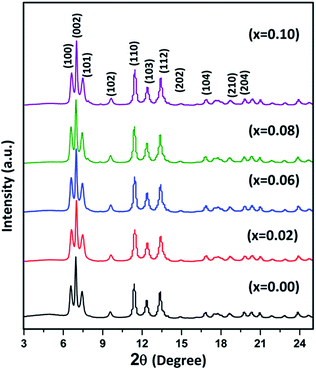
Synchrotron X-ray powder diffraction study
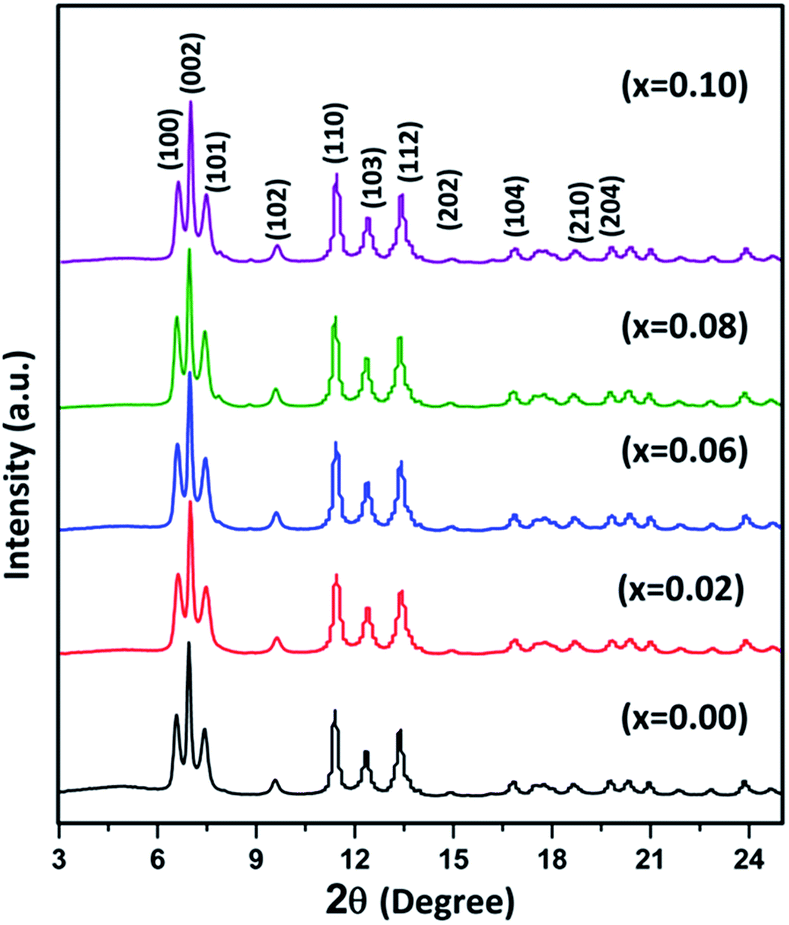
The synchrotron X-ray powder diffraction (SCXRPD) patterns of the pure and Co-doped ZnS NWs are shown in Fig. 1. The powder diffraction data were collected at a higher wave vector Q = 10.2 Å−1, which was recorded in the transmission mode using a shorter X-ray wavelength of 0.378377 Å at high energy ∼33 keV from beamline BL-11, AD/ED-XRD at RRCAT, Indore. The SCXRPD measurements were achieved with a highly monochromatic synchrotron beam using a Si (111) channel cut monochromator. The full scan SCXRPD is provided in the ESI Fig. S3.†
 |
| | Fig. 1 SCXRPD patterns of the Co-doped ZnS NWs. | |
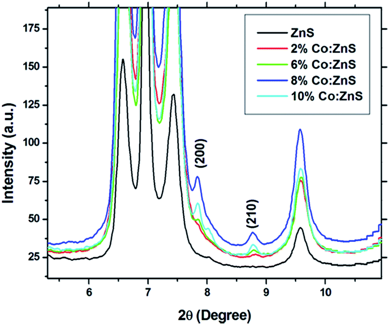
SCXRPD revealed the high resolution diffraction for the structural refinement. The entire diffraction peaks of the sample can be readily indexed as a wurtzite structure with the JCPDS card no. 36-1450. Secondary phases and extra peaks of the alloy or sulfide phases were detected in the case of the Co-doped ZnS samples due to the enhancement in solubility limit. It can be clearly observed from Fig. 2 that the peaks (200) and (210) for the CoS phases have a cubic structure and its plane values are indexed in accordance with the JCPDS card no. 83-0573. The intensity of the secondary phases is very low compared to the other peaks. The intensity of the secondary phase peaks for 8% Co doping is more than for 10% Co doping. When the dopant concentration reaches the maximum value of 10% and is reasoned as indicating an excess amount of Co2+, it readily reacts with the S2− ions in the medium, since the solubility and ionic product constants of CoS are greater than the solubility and ionic product constants of ZnS.
 |
| | Fig. 2 Magnified view (5°–11°) of Fig. 1 showing CoS phases with hkl (200) and (210) planes in the SCXRPD patterns of the Co-doped ZnS NWs. | |
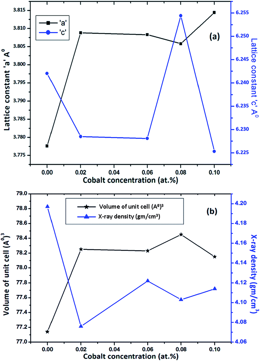
It can be noticed from Fig. 1 that the (002) peak becomes broadened in all the cases, and also this broadening can clearly be seen in Fig. 2 when this peak was magnified along with the relative intensity of peak (002), suggesting that the crystallinity of ZnS was degraded as a result of Co doping. It also indicates that the nanowires are grown in the (002) direction, which is further evidenced by the TEM analysis. The lattice constant, volume of unit cell, and X-ray density were calculated using the SCXRPD data and their values are plotted in Fig. 3. The volume of the unit cell increased while the X-ray density decreased in the pure and cobalt-doped ZnS samples. The values of 2θ in the XRD were shifted toward a lower angle side, which reflects the lattice expansion in the crystals. The lattice expansion can also be observed when the Co2+ ions substitute for the Zn2+ sites, since the ionic radius of the Co2+ ions (0.79 Å) is larger than that of the Zn2+ ions (0.75 Å).
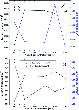 |
| | Fig. 3 (a) Lattice constant and (b) volume of unit cell and X-ray density for the pure and cobalt-doped ZnS NWs. | |
Atomic pair distribution function analysis
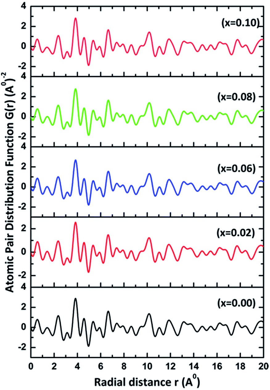
In order to obtain information on the local structure of the pure and Co-doped ZnS nanowires, SCXRPD and PDF techniques were employed in combination. The SCXRPD data were employed to obtain the PDF from the AD/ED-XRD BL-11 beamline at RRCAT, Indore. It can be seen in Fig. 4 that the as-synthesized nanowires show a series of well-defined peaks up to quite long real space distance, which means that the nanowires exhibit a medium-range periodic atomic order.16,30,37 The SCXRD patterns of the crystalline pure and Co-doped ZnS show well-defined Braggs peaks at Q = 10.2 Å−1. For manifestation of the pair distribution functions, the obtained data were corrected and normalized using the program PDFGetX3-1.1.38,39 The manifestation of the pair distribution function G(r) is the probability of finding a nearest neighbor at a certain distance ‘r’ between atoms.40,41 From the PDF patterns, spheralite and hexagonal structures were confirmed with the space groups F![[4 with combining macron]](https://www.rsc.org/images/entities/char_0034_0304.gif) 3m and P63mc, respectively. Sulfide and selenide semiconductor materials show two well-known structures, namely zinc blende and wurtzite structures, with identical shared tetrahedral bonding for different stacking sequences. The close-packed stacking sequence for the wurtzite structure is ABABAB… along the (001) orientation whereas for the zinc blende structure the close-packed stacking sequence is ABCABC… along the (111) orientation. Yang et al.43 and Masadeh et al.44 reported that CdSe nanoparticles show a mixed state of crystalline structures between zinc blende and wurtzite structures.42
3m and P63mc, respectively. Sulfide and selenide semiconductor materials show two well-known structures, namely zinc blende and wurtzite structures, with identical shared tetrahedral bonding for different stacking sequences. The close-packed stacking sequence for the wurtzite structure is ABABAB… along the (001) orientation whereas for the zinc blende structure the close-packed stacking sequence is ABCABC… along the (111) orientation. Yang et al.43 and Masadeh et al.44 reported that CdSe nanoparticles show a mixed state of crystalline structures between zinc blende and wurtzite structures.42
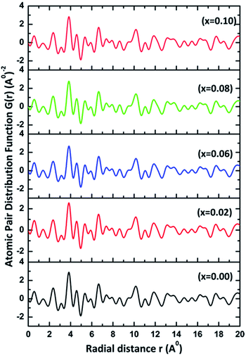 |
| | Fig. 4 The experimental pair distribution function G(r) of the pure and Co-doped ZnS NWs. | |
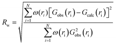
We obtained both the phases in the pure and Co-doped ZnS NWs after refinement/modeling due to inhomogeneity in the crystal structure at the nanoscale with constrain isotropic ADPs for the spheralite structure and anisotropic ADPs for the wurtzite structure. Also the results for the modeling of structures of the samples with respect to the unit cell parameter, ADPs, z-coordinate of S, scale factor, resolution damping factor (Qdamp), and resolution peak broadening factor (Qbroad) are depicted in Table 1. The sharp and well-resolved peaks in PDF suggest a high symmetry and a well-defined local structure of the NW samples. These peaks are broader, reflecting the presence of a considerable local structural disorder and strain in the as-synthesized samples. The PDFs are shown in Fig. 4, which also gives the interatomic distances from the peak values. From Fig. 5, the first nearest cation–anion, second cation–cation, and third anion–anion neighboring distances of the pure and Co-doped ZnS NWs are tabulated in Table 1. The cation–anion distance of the Zn2+–S2− bonded pair is between 2.3050 and 2.3369 Å for the hexagonal and 2.3466 to 2.3511 Å for the spheralite covalently bonded pair in the samples. From the first neighbor, it can be predicted that these bond length values are highly correlated. The second strong and intense peak is of the metal–metal bonding distance at 3.7733 to 3.835 Å, which reflects the cation–cation Zn2+/Co2+–Zn2+ neighbors of the pure and Co-doped ZnS samples. It was visualized that the finite particle size or diameter is evident in a fall-off in the intensity of the structural features with increasing the radial distance. The average diameters of the pure and Co-doped ZnS NWs were also extracted from the refined PDF and are depicted in Table 1. Quantitative structural information can be extracted from refinement of PDF by comprising data from the observed PDF and the calculated PDF from the models. The PDFgui53 computer program was used to fit and simulate the structural model to the experimental PDF, as shown in Fig. 5. Fig. 5 reflects the wurtzite structure over the wurtzite modeling using isotropic ADPs. These give a best fit for structures from the experimental and calculated PDFs from refinement, which is in agreement with the residual function. It was corroborated from Fig. 5 the good fit of the wurtzite structure model over the wurtzite structure. In Fig. 5, we observed some peaks matched to a certain extent of ‘r’, which means that there is possibility of multi-phases for the same structures at certain neighboring distance. The values of the refined parameters are summarized in Table 1 for their respective fit manifested in Fig. 5. The refinement of the calculated PDF to the experimental PDF was characterized by the residual function (Rw)43 using eqn (1):
| |
 | (1) |
where
Gobs is the PDF extracted from the diffraction data,
Gcal is the PDF calculated from the model, and
ω(
ri) is the weight. The structural parameters of the model were the unit cell parameter, and the anisotropic atomic displacements (ADPs) for Zn and S. A generated simulated PDF from calculated data which is well matched with the experimental data. The resulting very low residual signal intensity across the fitting range for pure and Co-doped ZnS NWs for hexagonal structure showed
Rw = 0.247, 0.282, 0.267, 0.258, and 0.297 (with the fitting range of 1.7 to 20 Å), respectively. The
Rw values and their respective refined parameter results are listed in
Table 1.
Fig. 5 explicitly shows the wurtzite model, which gives a better fit. The as-synthesized NWs structures do not purely belong to wurtzite or spheralite structures, but reflect intermediate structures/mixed structures.
Table 1 The refined parameters of the pure and Co-doped ZnS NWs obtained using PDF analysis
| Structures |
Structural parameters |
Pure ZnS |
2% Co:ZnS |
6% Co:ZnS |
8% Co:ZnS |
10% Co:ZnS |
| Hexagonal |
a (Å) |
3.8343(5) |
3.8340(6) |
3.8305(4) |
3.8356(4) |
3.8109(4) |
| c (Å) |
6.2708(2) |
6.2938(2) |
6.2619(1) |
6.2755(1) |
6.2576(1) |
| Unit cell volume |
79.84(4) |
80.12(5) |
79.57(4) |
79.95(3) |
78.16(4) |
Co/Zn U11![[double bond, length as m-dash]](https://www.rsc.org/images/entities/char_e001.gif) U22 U22 |
0.0059(2) |
0.0065(2) |
0.0052(1) |
0.00518(1) |
0.0033(1) |
| U33 |
0.0080(4) |
0.0165(8) |
0.0049(1) |
0.00641(2) |
0.0041(3) |
| S U11U22 |
0.0012(3) |
0.0012(4) |
0.0013(1) |
0.0012(1) |
0.0012(2) |
| U33 |
0.0639(4) |
0.0023(1) |
0.0568(2) |
0.0688(2) |
0.0086(8) |
| S Zfrac |
0.3862(6) |
0.3873(6) |
0.3850(2) |
0.3810(5) |
0.3781(6) |
| Qdamp |
0.0436(2) |
0.0900(1) |
0.0427(2) |
0.0317(2) |
0.1594(7) |
| Qbroad |
0.0745(4) |
0.1235(4) |
0.1091(3) |
0.0989(3) |
0.0737(2) |
| Scale factor |
0.3052(3) |
0.3081(2) |
0.4021(3) |
0.4148(3) |
0.4536(4) |
| Zn–S |
2.3359(1) |
2.3244(1) |
2.3258(1) |
2.3269(1) |
2.3050(1) |
| Co/Zn–Zn |
3.8343(5) |
3.8340(1) |
3.8305(6) |
3.8326(8) |
3.7733(9) |
| S–S |
5.4253(1) |
5.4317(1) |
5.4191(1) |
5.4278(6) |
5.4978(3) |
| Rw |
0.247 |
0.282 |
0.267 |
0.258 |
0.297 |
| Diameter (nm) |
9.4(2) |
11.2(2) |
12.5(3) |
12.6(2) |
12.9(4) |
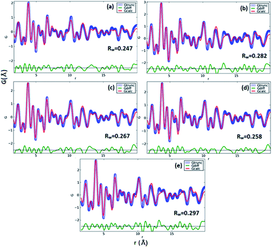 |
| | Fig. 5 The experimental PDF G(r) and calculated refined PDF with the difference curve offset given below. PDF refinement fitting using the wurtzite structure (a)–(e) model with the space group P63mc and anisotropic ADPs of the pure and Co-doped ZnS NWs, respectively. | |
The strain in nanostructures has been observed by different researchers, where alternative techniques were used to investigate the size-induced strain in nanostructured materials.43 The atomic structure of Co-doped ZnS NWs was subjected to different types of structural distortions relative to the corresponding pure ZnS NW materials. This approach was based on the first PDF-peak analysis, in terms of the position and width, where the local bonding of the basic building unit was investigated as a function of the nanowire diameter. The width and position could be extracted by fitting Gaussian functions,44 even without any knowledge about the adopted symmetry or atomic structure type. The first local bonding of the cation and anion of the tetrahedral (Zn2+/Co2+–S2−) building unit was investigated vs. the nanoparticle diameter. The nearest first neighbor peaks at r = 2.336 Å come from covalently bonded Zn2+–S2− pairs. The positions and the width of these peaks were determined by fitting a Gaussian plot of ESI Fig. S4† and the results are presented in Table 2. The results outline that there is an interesting compressive strain on this nearest-neighbor bond length, which is possible to measure with the PDF in a high accuracy. It was observed that internal strain deceases rapidly with an enhancing NW diameter. The bond length of Zn–S pairs shortens as the NWs diameters enhance, which suggest the presence of an internal stress in the NWs. The Zn–S bond lengths extracted from the PDF structural refinement were also in good agreement with those obtained from the first-peak Gaussian fit, as shown in the ESI Fig. S4.† Apparently, there was no size-dependent homogeneous strain measurable on the first peak.
Table 2 The first PDF-peak position (FPP) and width (FPW) for the pure and Co-doped ZnS nanowires
| |
Pure ZnS |
2% Co:ZnS |
6% Co:ZnS |
8% Co:ZnS |
10% Co:ZnS |
| PDF FPP |
2.3375 |
2.3320 |
2.3286 |
2.3232 |
2.3173 |
| PDF FPW |
0.4451 |
0.4359 |
0.4449 |
0.4515 |
0.4575 |
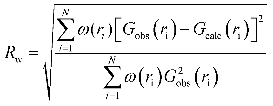
Micro-Raman spectroscopic study
Micro-Raman measurements of the as-synthesized samples were carried out using an excitation laser wavelength of argon 488 nm to study the effects of the cobalt-substituted ZnS NWs. The background subtracted/corrections Raman spectra data for the as-synthesized NWs are shown in Fig. 6. It is known that the wurtzite ZnS belongs to the symmetric space group C46ν (P63mc) in the primitive cell. The zone-center optical phonon can be classified as the following irreducible representation:| | |
Γopt = A1 + E1 + 2E2 + 2B1
| (2) |
where, A1 and E1 are polar modes and both are Raman and infrared active, while the E2 modes are nonpolar and Raman active only and the B1 modes are silent modes. The longitudinal optic (LO) peaks have been reported to center at around 350 cm−1 for both hexagonal and cubic structures of ZnS.45 For the samples of Zn1−xCoxS of NWs with Co concentrations at x = 0.02, 0.06, and 0.08, sharp peaks could be clearly observed at 246.77, 249.02, and 250.15 respectively. Jimenez-Sandoval et al.46 reported 3 peaks in the range of spectral region, i.e., transverse optic (TO) (276) to LO (350 cm−1) for the TM (Co2+, Fe2+, Mn2+, etc.)-substituted ZnS nanomaterials. In this article, only two peaks appeared in that region at 313.60, 333.16 cm−1, and 306.7, 329.90 cm−1, while the peak at 300 cm−1 was not observed for 0.02 and 0.06 respectively. In the case of 8% Co-doped ZnS, peaks at 333.16 and 302.06 cm−1 were observed. Furthermore, for all the samples, the peaks at 349.34, 347.08, and 344.70 cm−1 were assigned to strong first-order scattering from an unresolved doublet, which identifies the A1 and E1 symmetry LO phonon vibration modes. It was confirmed the E1 (LO) mode results from the lateral morphology of the Co-doped ZnS nanowires parallel to the c-axis,47 and in addition, strong surface optical (SO) phonon modes were observed at 330 and 333 cm−1.45–47 As compared to the Raman spectrum of bulk hexagonal ZnS (LO: 352 cm−1) (Brafman et al.48 and Nilsen et al.49), the peaks of the first-order LO phonons from these ZnS nanowires exhibit a shift toward lower energy. The red-shift of the LO mode in the samples indicates that a tensile strain existed in the lattice. Due to the limited solubility of Co ions in ZnS (2%), it was expected the Co ions would be located interstitially in the lattice instead of being substituted for Zn2+ as the Co concentration increased. Therefore, the gradual shift of the LO mode as well as the tensile strain with increasing Co content are believed to result from the excess incorporation of Co interstitially in the ZnS lattice. This strain effect could also be validated by observation of the broadening LO peak value with the increasing Co content, as shown in Fig. 6. This also confirmed the strain of the samples using the PDF analysis given in the ESI Fig. S4.† The minor peaks were clearly identified for the mode at ∼213.29, 222.44 and 223.69 cm−1 corresponding to the second-order longitudinal acoustic (2LA) phonon in Co:ZnS NWs,45 together with a sharp peak at 276.73 cm−1, which consists of the assigned modes of A1(TO). It is also observed that the broad peak at 673.35 in 8% Co:ZnS NWs could be assigned to second-order LO. Kumar et al.50 reported that the coupling between longitudinal phonons and charge density modes, namely L+ and L− modes, were detected. As the charge carrier concentration in the semiconductor increases, the frequency of the L+ mode increases from bulk LO mode frequency, while the frequency of the L− mode increases from zero to the TO mode frequency.50 Hence the peaks at 246.8, 249, and 250.15 cm−1 observed in the present samples can be tentatively attributed to the LOPC (L−) mode,57 which may be due to the formation of a small portion of the intermediate state due to the uncompleted conversion during the synthesis process. It can be observed from Fig. 6 that the LO mode is more altered while the peak position of the LOPC mode has shifted to higher frequencies with the increase in cobalt concentrations, which is attributed to the decrease in carrier concentration, which reveals the existence of free electrons by Co+ ions. In addition, second-order Raman scattering is seen in the range of 350–450 cm−1. This second-order scattering consist of a TO + transverse acoustic (TA) phonon mode at ∼393 cm−1 for 6% Co:ZnS NWs. It is similar to the 2LA phonon response and multiphonon response in the range of 350–450 cm−1 which is observed because the strong plasmons background fluctuations in polar semiconducting systems result in two different LOPC modes.
 |
| | Fig. 6 Room temperature micro-Raman spectra of first-order TO and LO phonons modes for 2%, 6%, 8% Co:ZnS NWs. The genuine feature of a spectral line observed at ∼250 cm−1 for the LOPC mode. | |
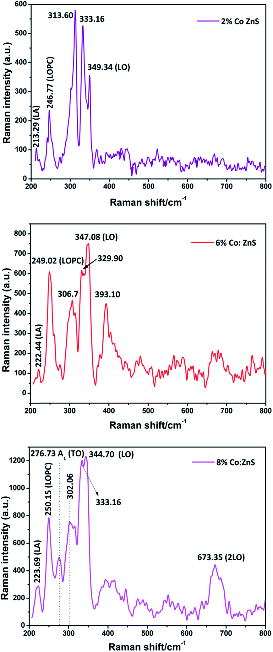
Morphological study
The nanowires assembled into micrometer-diameter-sized spheres or flowers of the pure and Co-doped ZnS samples are shown in Fig. 7. Fig. 8 shows the micrographs of the as-synthesized samples, where it is quite clear that the NWs structure is assembled into micro-flowers with a high aspect ratio. TEM images of the as-synthesized samples are shown in Fig. 8. The TEM micrographs show the extremely uniform diameter of the nanowire micro-flowers. The average diameters of the pure and Co-doped ZnS NWs were found to be 8.18, 12.31, 12.71, and 14.44 nm with lengths of tens of micrometers respectively. The average diameter of the undoped and Co-doped ZnS micro-flowers was evaluated to be 1200 nm using FE-SEM and TEM micrographs. Selected-area electron diffraction (SAED) pattern were taken from the nanowires of the micro-flowers of 6% Co:ZnS, which suggest it has a single crystal nature. The spots on the SAED patterns can be easily attributed to the [110] zone axis of the nanowires. The compositional analysis of the pure and Co-doped ZnS NWs was obtained from the energy-dispersive absorption X-ray (EDAX) and XPS spectra of the samples, as shown in the ESI Fig. S1 and S2,† respectively, and the FTIR spectra are also given in the ESI Fig. S5;† it can be noticed that the peaks of Zn, S, and Co are present. For the pure ZnS structure, qualitative analysis reveals that the atomic ratio of Zn to S is very close to 1:1 stoichiometrically. For 2% Co-doped ZnS NWs, the atomic% of Zn, Co, and S was found to be 50.55, 0.63, and 48.82, respectively, whereas for 6% and 10% Co:ZnS NWs the atomic% of the elements of Zn, Co, and S was found to be 50.88, 2.02, 46.50 and 49.75, 3.59, 46.66, respectively. The amount of Co element detected was less than that actually added during synthesis.
 |
| | Fig. 7 (a–e) FE-SEM images of the pure and Co-doped ZnS NWs. | |
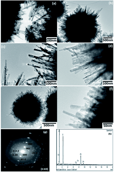 |
| | Fig. 8 TEM images of the Co-doped ZnS NWs as (a) and (b) images for pure ZnS (c) for 0.06 Co:ZnS, (d), (e) for 0.08 Co:ZnS, (f) for 0.10, (g) and (h) SAED pattern and EDAX spectra corresponding to 0.06 Co:ZnS micro-flower nanowires. | |
Optical study
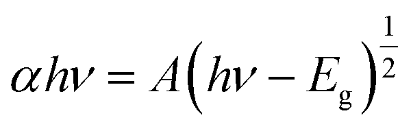
The UV-visible absorption spectra of the pure and Co-doped ZnS NWs are shown in Fig. 9. The absorption peaks were observed at 385.95 nm, 416.05 nm, 420.06 nm, 438 nm, and 448 nm for the pure and Co-doped ZnS NWs, respectively. A red-shift was observed at the absorption edge to the smaller wavelength side, which was due to exchange interactions between the d-electrons of cobalt ions and the s and p electrons of the host electron band. The pure and Co-doped ZnS samples show a red-shift comparable to bulk ZnS (345 nm). This red-shift can be attributed to the quantum confinement effect in the NWs. The energy band gap was calculated from the Tauc eqn (3):51| |
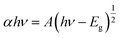 | (3) |
where α is the absorption coefficient, hν is the photon energy, A is the constant, and Eg is the energy band gap of the sample. ZnS has a direct band gap, hence the value of n is ½, because transition from the valence band to conduction band is direct. The energy band gaps of the pure and Co-doped ZnS samples were found to be 3.25, 3.05, 2.99, 2.94, and 2.83 eV, respectively. The Co2+ ions substitution in the ZnS lattice effects the sp–d exchange interaction between the band electrons and the localized d-electron of the Co2+ ions. The calculated energy bandgap of the samples was found to be decrease with the increase in Co2+ content; this was attributed to the negative and positive correction to the conduction and valence band edges, which arise from the s–d and p–d interactions, respectively, resulting in shrinkage of the bandgap.52
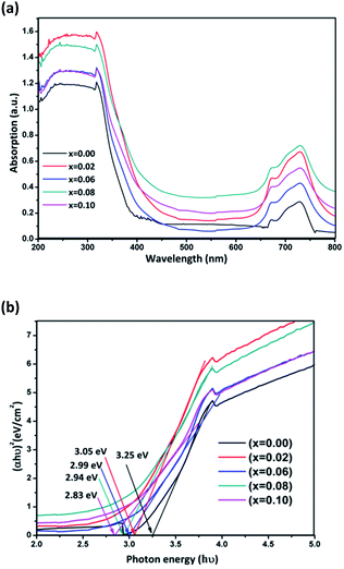 |
| | Fig. 9 (a) Absorption spectra of the pure and cobalt-doped ZnS NWs. (b) Tauc plots of the pure and cobalt-doped ZnS NWs. | |
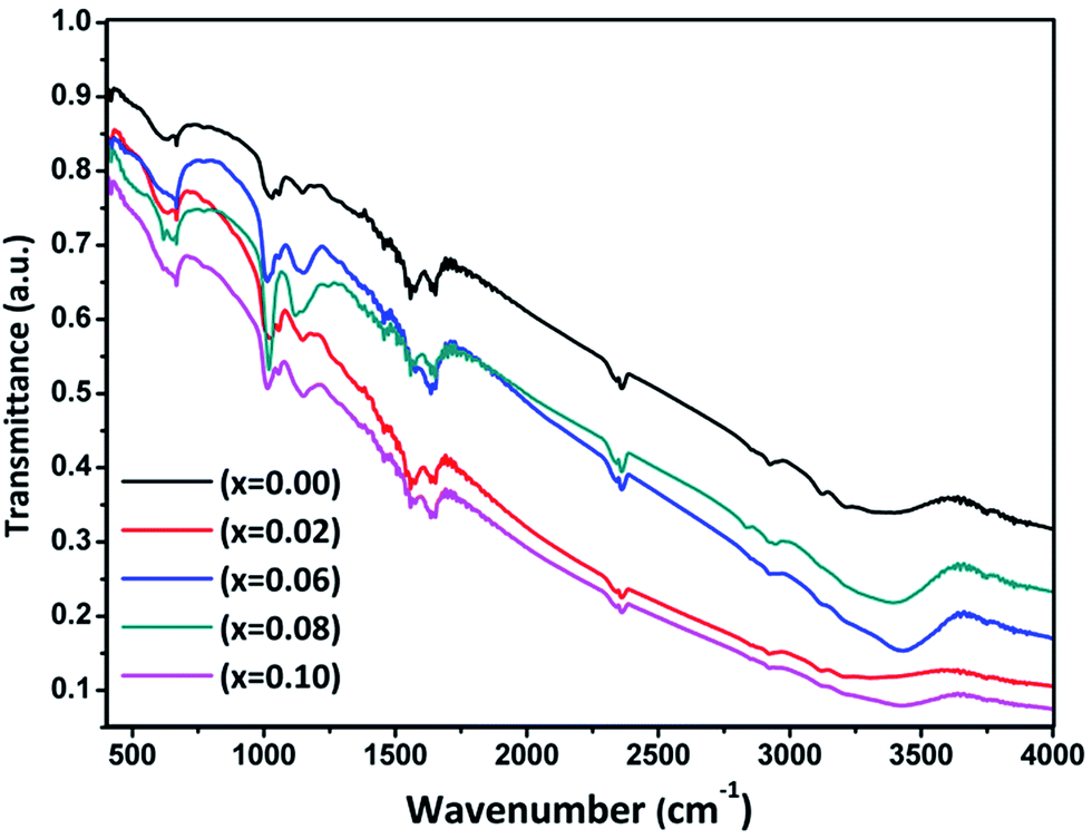
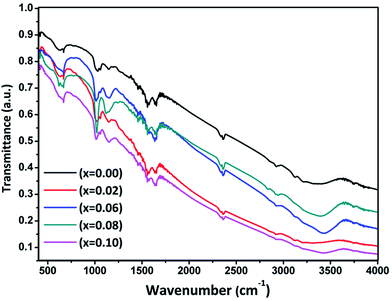
FTIR study
FTIR transmittance spectra for the pure and Co-doped ZnS samples are shown in Fig. 10. The sharp and strong peaks also show the samples were highly crystalline in nature. There were only a few peaks observed at 400–4000 cm−1. It is well known that an absorption peak at 400–650 cm−1 indicates Zn and S stretching;54 here, we also observed peaks for pure and Co-doped ZnS NWs at 416.58, 666.30 cm−1; 419.43, 670.53 cm−1; 419.33, 662; 419.43, 626.33 cm−1; and 410.97, 652.66 cm−1; respectively. This indicates the formation of pure and cobalt-doped ZnS NWs. The absorption bands at 2359 to 2923 cm−1 were attributed to –C–H vibration,55 which were observed due to the doping of cobalt. The observed values at 3215 to 3321 cm−1 indicate OH stretching. The peaks at 1038.5,1163; 1027, 1150; 1011, 1150; 1019.4, 1133 cm−1; and 1011, 1158 cm−1 were observed due to the formation of micro-structures for the pure and Co-doped ZnS samples, respectively;55,56 whereas, the –NH2 stretching, scissor vibrations, and C–N stretching vibration at 1000 to 1160 cm−1 appeared in the FTIR spectra.56 The bands at 1550 to 1658 cm−1 are due to the –CO stretching mode, arising from the absorption of atmospheric CO2 on the surface of the samples (Qadri et al.).55 The band values are in good agreement with those reported in the literature.55–58 The close similarity in the FTIR spectra of pure and Co-doped ZnS NWs outlines that Co is substituted into the ZnS lattice without altering the crystal structure.
 |
| | Fig. 10 FTIR spectra of the pure and Co-doped ZnS NWs. | |
Conclusions
In conclusion, the samples of pure and cobalt-doped ZnS micro-flower nanowires were successfully synthesized by a hydrothermal method. Synchrotron X-ray powder diffraction data were employed for analysis of the pair distribution function (PDF). The PDF was utilized to address the atomic-scale structure of the as-synthesized NWs. The interatomic distance was calculated considering the PDF analysis. Total X-ray diffraction coupled to PDF data analysis allows the determination of the presence of nanoscale inhomogeneity in the structure. The internal strain was extracted from PDF as a function diameter of the nanowires and showed that the internal strain increased with Co doping due to the enhancement in the diameter of the nanowires. It was observed from the FE-SEM and TEM image analyses that the morphology of the as-synthesized samples showed the NWs structure was assembled into micro-size flower (clusters of nanowires)-like shapes. The Raman spectra were obtained for the pure and Co-doped ZnS NWs, which exhibited second-order longitudinal acoustic (2LA) phonon modes at ∼213.29, 222.44, and 223.69 cm−1, first-order phonon modes at 349.34, 347.08, and 344.70 cm−1 corresponding to A1/E1 longitudinal-optical-phonon vibration modes, and a strong surface optical (SO) phonon mode observed at 330 to 333 cm−1. The LOPC (L−) mode was observed due to free electrons from the Co+ ions. EDAX and XPS studies showed the successful doping of cobalt. The energy band gap of cobalt-doped ZnS samples showed a red-shift as compared to the bulk ZnS band gap. Also the size of nanowires increase with the increasing cobalt content, which reduced the band gap. It was confirmed from the FTIR study that cobalt substitutes to the ZnS site. The combination of synchrotron X-ray diffraction and atomic PDF shows potential as a tool for the standardization of the atomic-scale structure of nanomaterials.
Acknowledgements
The authors are grateful to Prof. S. S. Shah for his encouragement. Also the authors are thankful to Dr K. K. Pandey High Pressure &Synchrotron Radiation Physics Division, Bhabha Atomic Research Centre, Mumbai (India) for availing beamline BL-11 for SCXRPD facility, Dr N. P. Lalla and Dr U. P. Deshpande UGC-DAE CSR, University Campus, Khandwa Road, Indore (India) for providing TEM and XPS, UV-Vis, FTIR facilities.
References
- P. Jiang, J. Jie, Y. Yu, Z. Wang, C. Xie, X. Zhang, C. Wu, L. Wang, Z. Zhu and L. Luo, J. Mater. Chem., 2012, 22, 6856 RSC.
- C. Wu, J. Jie, L. Wang, Y. Yu, Q. Peng, X. Zhang, J. Cai, H. Guo, D. Wu and Y. Jiang, Nanotechnology, 2011, 22, 069801 CrossRef.
- H. Ong and R. Chang, Appl. Phys. Lett., 2001, 79, 3612–3614 CrossRef CAS.
- T. Tran, W. Park, W. Tong, M. Kyi, B. Wagner and C. Summers, J. Appl. Phys., 1997, 81, 2803–2809 CrossRef CAS.
- Z. Zhong, Science, 2003, 302, 1377–1379 CrossRef CAS PubMed.
- Y. Cui, Z. Zhong, D. Wang, W. Wang and C. Lieber, Nano Lett., 2003, 3, 149–152 CrossRef CAS.
- O. Shirak, O. Shtempluck, V. Kotchtakov, G. Bahir and Y. Yaish, Nanotechnology, 2012, 23, 395202 CrossRef CAS PubMed.
- P. Calandra, M. Goffredi and V. Liveri, Colloids Surf., A, 1999, 160, 9–13 CrossRef CAS.
- Y. Cui, Science, 2001, 293, 1289–1292 CrossRef CAS PubMed.
- Z. Chen, L. Cheng, H. Xu, J. Liu, J. Zou, T. Sekiguchi, G. Lu and H. Cheng, Adv. Mater., 2010, 22, 2376–2380 CrossRef CAS PubMed.
- Q. Wang, B. Liu, X. Wang, S. Ran, L. Wang, D. Chen and G. Shen, J. Mater. Chem., 2012, 22, 21647 RSC.
- M. Ruedas-Rama, A. Orte, E. Hall, J. Alvarez-Pez and E. Talavera-Rodriguez, Biophys. J., 2011, 100, 468a–469a CrossRef.
- S. Acharya, N. Maheshwari, L. Tatikondewar, A. Kshirsagar and S. Kulkarni, Cryst. Growth Des., 2013, 13, 1369–1376 CAS.
- M. Limaye, S. Gokhale, S. Acharya and S. Kulkarni, Nanotechnology, 2008, 19, 415602 CrossRef PubMed.
- D. Wu, Y. Jiang, Y. Zhang, Y. Yu, Z. Zhu, X. Lan, F. Li, C. Wu, L. Wang and L. Luo, J. Mater. Chem., 2012, 22, 23272 RSC.
- J. Kim, S. Kim, D. Kim, K. Oh, W. Hong, T. Bae and H. Chung, J. Nanomater., 2016, 2016, 1–6 Search PubMed.
- U. Gawai, H. Khawal, T. Shripathi and B. Dole, CrystEngComm, 2016, 18, 1439–1445 RSC.
- S. Kar and S. Chaudhuri, J. Phys. Chem. B, 2005, 109, 3298–3302 CrossRef CAS PubMed.
- S. Acharya, S. Bhoga and K. Singh, Integr. Ferroelectr., 2010, 116, 16–22 CrossRef CAS.
- S. Pahari, A. Sinhamahapatra, N. Sutradhar, H. Bajaj and A. Panda, Chem. Commun., 2012, 48, 850–852 RSC.
- W. Xuan-Rong, Y. Qiao-Zhen, Z. Yong-Xiang and L. Yan-Luo, J. Inorg. Mater., 2016, 31, 473 CrossRef.
- M. Wei, J. Yang, Y. Yan, J. Cao, Q. Zuo, H. Fu, B. Wang and L. Fan, Superlattices Microstruct., 2013, 54, 181–187 CrossRef CAS.
- J. Cao, L. Fan, J. Yang, Y. Yan, M. Wei, L. Yang, B. Feng, D. Han, B. Wang and H. Fu, Superlattices Microstruct., 2013, 57, 58–65 CrossRef CAS.
- M. Lu, L. Chen, W. Mai and Z. Wang, Appl. Phys. Lett., 2008, 93, 242503 CrossRef.
- X. Xu, G. Fei, W. Yu, X. Wang, L. Chen and L. Zhang, Nanotechnology, 2005, 17, 426–429 CrossRef.
- R. Chen, D. Li, B. Liu, Z. Peng, G. Gurzadyan, Q. Xiong and H. Sun, Nano Lett., 2010, 10, 4956–4961 CrossRef CAS PubMed.
- C. Bradford, C. O'Donnell, B. Urbaszek, A. Balocchi, C. Morhain, K. Prior and B. Cavenett, J. Cryst. Growth, 2001, 228, 634–638 CrossRef.
- M. Navaneethan, J. Archana, K. Nisha, Y. Hayakawa, S. Ponnusamy and C. Muthamizhchelvan, Mater. Lett., 2012, 68, 78–81 CrossRef CAS.
- M. Huang, Y. Cheng, K. Pan, C. Chang, F. Shieu and H. Shih, Appl. Surf. Sci., 2012, 261, 665–670 CrossRef CAS.
- U. Gawai, H. Khawal, M. Bodke, K. Pandey, U. Deshpande, N. Lalla and B. Dole, RSC Adv., 2016, 6, 50479–50486 RSC.
- V. Petkov, Mater. Today, 2008, 11, 28–38 CrossRef CAS.
- V. Petkov, K. Rangan, M. Kanatzidis and S. Billinge, Mater. Res. Soc. Symp. Proc., 2001, 678 Search PubMed.
- C. Ho, P. Varadhan, H. Wang, C. Chen, X. Fang and J. He, Nanoscale, 2016, 8, 5954–5958 RSC.
- M. Seong, S. Chun, H. Cheong, N. Samarth and A. Mascarenhas, Phys. Rev. B: Condens. Matter Mater. Phys., 2002, 66, 033104 CrossRef.
- Y. Lin, C. Chiu, W. Fan, C. Chia, S. Yang, D. Chuu, M. Lee, W. Chen, W. Chang and W. Chou, J. Appl. Phys., 2007, 102, 123510 CrossRef.
- H. Harima, S. Nakashima and T. Uemura, J. Appl. Phys., 1995, 78, 1996–2005 CrossRef CAS.
- M. Feygenson, J. Neuefeind, T. Tyson, N. Schieber and W. Han, Inorg. Chem., 2015, 54, 11226–11235 CrossRef CAS PubMed.
- V. Petkov, T. Ohta, Y. Hou and Y. Ren, J. Phys. Chem. C, 2007, 111, 714–720 CAS.
- P. Juhás, T. Davis, C. Farrow and S. Billinge, J. Appl. Crystallogr., 2013, 46, 560–566 CrossRef.
- K. Page, T. Hood, T. Proffen and R. Neder, J. Appl. Crystallogr., 2011, 44, 327–336 CrossRef CAS.
- S. Billinge and M. Kanatzidis, ChemInform, 2004, 35, 345–360 CrossRef.
- T. Egami and S. Billinge, Mater. Today, 2003, 6, 57 CrossRef.
- X. Yang, A. Masadeh, J. McBride, E. Božin, S. Rosenthal and S. Billinge, Phys. Chem. Chem. Phys., 2013, 15, 8480 RSC.
- A. Masadeh, E. Božin, C. Farrow, G. Paglia, P. Juhas, S. Billinge, A. Karkamkar and M. Kanatzidis, Phys. Rev. B: Condens. Matter Mater. Phys., 2007, 76, 113101 CrossRef.
- J. Kim, H. Rho, J. Kim, Y. Choi and J. Park, J. Raman Spectrosc., 2012, 43, 906–910 CrossRef CAS.
- S. Jiménez-Sandoval, A. López-Rivera and J. Irwin, Phys. Rev. B: Condens. Matter Mater. Phys., 2003, 68, 052101 CrossRef.
- H. Lu, S. Chu and C. Chang, J. Cryst. Growth, 2005, 280, 173–178 CrossRef CAS.
- O. Brafman and S. Mitra, Phys. Rev., 1968, 171, 931–934 CrossRef CAS.
- W. Nilsen, Phys. Rev., 1969, 182, 838–850 CrossRef CAS.
- S. Kumar, M. Khadar, S. Dhara, T. Ravindran and K. Nair, Nucl. Instrum. Methods Phys. Res., Sect. B, 2006, 251, 435–440 CrossRef CAS.
- J. Tauc, R. Grigorovici and A. Vancu, Phys. Status Solidi B, 1966, 15, 627–637 CrossRef CAS.
- L. Li, H. Liu, X. Luo, X. Zhang, W. Wang, Y. Cheng and Q. Song, Solid State Commun., 2008, 146, 420–424 CrossRef CAS.
- C. Farrow, P. Juhas, J. Liu, D. Bryndin, E. Božin, J. Bloch, T. Proffen and S. Billinge, J. Phys.: Condens. Matter, 2007, 19, 335219 CrossRef CAS PubMed.
- S. Ummartyotin, N. Bunnak, J. Juntaro, M. Sain and H. Manuspiya, Solid State Sci., 2012, 14, 299–304 CrossRef CAS.
- A. Mandal, A. Dandapat and G. De, Analyst, 2012, 137, 765–772 RSC.
- S. Qadri, E. Skelton, D. Hsu, A. Dinsmore, J. Yang, H. Gray and B. Ratna, Phys. Rev. B: Condens. Matter Mater. Phys., 1999, 60, 9191–9193 CrossRef CAS.
- J. Wang, T. You, H. Feng, K. Chen and B. Xu, J. Cryst. Growth, 2013, 374, 60–64 CrossRef CAS.
- U. Gawai, U. Deshpande and B. Dole, RSC Adv., 2017, 7, 12382–12390 RSC.
Footnote |
| † Electronic supplementary information (ESI) available: XPS and EDAX spectra were provided in Fig. S1 and S2 for details information. Also the full scan SCXRPD was provided in Fig. S3 with tabulated values in Tables S1 and S2 for pure and Co doped ZnS NWs. The first peak fitted with Gaussian, first PDF peaks width and strain in Zn–S bond given in Fig. S4. See DOI: 10.1039/c7ra02668d |
|
| This journal is © The Royal Society of Chemistry 2017 |
Click here to see how this site uses Cookies. View our privacy policy here. 
 Open Access Article
 This Open Access Article is licensed under a
  *
*