
 Open Access Article
 This Open Access Article is licensed under a
 Creative Commons Attribution 3.0 Unported Licence
Impact of interfacial effects on ferroelectric resistance switching of Au/BiFeO3/Nb:SrTiO3(100) Schottky junctions†
Shumin He‡
a,
Guolei Liu *a,
Yinlian Zhub,
Xiuliang Mab,
Jirong Sunc,
Shishou Kanga,
Shishen Yana,
Yanxue Chena,
Liangmo Meia and
Jun Jiaod
*a,
Yinlian Zhub,
Xiuliang Mab,
Jirong Sunc,
Shishou Kanga,
Shishen Yana,
Yanxue Chena,
Liangmo Meia and
Jun Jiaod
aSchool of Physics, State Key Laboratory of Crystal Materials, Shandong University, Jinan 250100, China. E-mail: liu-guolei@sdu.edu.cn
bShengyang National Laboratory for Materials Science, Institute of Metal Research, Chinese Academy of Sciences, Shenyang 110016, China
cBeijing National Laboratory for Condensed Matter Physics and Institute of Physics, Chinese Academy of Science, Beijing 100190, China
dDepartment of Mechanical and Materials Engineering, Portland State University, P.O. Box 751, Portland, OR 97207-0751, USA
First published on 26th April 2017
Abstract
Direct evidence of purely interfacial effects on resistance switching is demonstrated in Au/BiFeO3/Nd:SrTiO3(001) (Au/BFO/NSTO) Schottky junctions by reducing the thickness of ferroelectric interlayer BFO. The Au/BFO/NSTO junction shows large current rectification and hysteretic resistive switching behavior without any electroforming process. The conduction mechanism is dominated by interface-limited Fowler–Nordheim (FN) tunneling through a potential barrier formed at the BFO/NSTO interface. Measurements of polarization switching dynamics and capacitance–voltage characteristics provide direct evidence that the resistance switching in the Au/BFO/NSTO junction is ferroelectric and interfacially limited. The observed resistance switching behavior can be attributed to the ferroelectric polarization modulation of the barrier and depletion width of the p–n junction formed at the BFO/NSTO interface.
I. Introduction
As the conventional semiconductor memory technologies are approaching their scaling limits, nonvolatile resistive random access memory (RRAM) is considered as one of the promising candidates for the next generation of nonvolatile memory, due to its high-speed operation, low power consumption, and compatibility with complementary metal-oxide semiconductor integration processes.1,2 Resistive switching (RS) behaviors and memristive behaviors been investigated in many materials, e.g., binary transition metal oxides,2,3 perovskite type oxides,4,5 and some other materials.6,7 Ferroelectric resistive switching (FeRS) consisting of metal/ferroelectrics/metal (MFM) structures has also attracted considerable attention.8 In contrast to other resistive memories consisting of 3d transition metal oxides like TiO2 and ZnO,2,3 FeRS is based on intrinsic switchable ferroelectric polarization in the ferroelectric materials,9 rather than a voltage-induced migration of matter at nanoscale.10,11Recently, the ferroelectric polarization modulated switchable diode effects and resistance switching behaviors have been discovered and investigated in multiferroic BiFeO3 (BFO) based MFM structures.4,8,12–27 The observed RS behaviors in BFO films appear to vary with the forming processing conditions and microstructures of the BFO film, which suggests that several mechanisms may be involved. Possible mechanisms proposed by previously reported studies can be classified into two types: (1) conductive filament type in polycrystalline BFO films, where the local conductive paths consisting of oxygen vacancies or metallic filaments are formed at low resistance state (LRS), and damaged at high resistance state (HRS).21,25–27 (2) Ferroelectric polarization modulated interfacial resistance switching, where a Schottky junction or a p–n junction may be formed at the BFO/metal interface or the BFO/n-type semiconductor interface, respectively.4,17,22–24 Reversing the ferroelectric polarization, it induces a blocking or non-blocking interface for the transit carriers and consequently the resistance switching behaviors of low or high resistance states. Though the electrical properties of BFO-based MFM structures are critically affected by the electrodes and metal/BFO interface, the role of interfacial effect on the RS behaviors is still a challenging topic. Many previously studies focusing on significantly thicker BFO films with a large suppression of bulk-limited leakage current, where the fitting of LRS by ohmic or the space-charge-limited current (SCLC) and HRS by Schottky emission is a well-known signature of an interface based conduction mechanisms.4,17,22–24 However, these interfacial effects was not separated from that of the bulk of BFO film in cases of resistance and capacitance,4,17,22–24 as a result, one could not conclude that LRS and HRS were only due to the interface effects. Also it is necessary to check the direct link between RS and Schottky barrier (or p–n junction) at interface.
In this study, we restrict the thickness of BFO film to such a dimension, where the volume fractions of BFO film could be significantly modulated under depletion or accumulation conditions by ferroelectric polarization reversals. Therefore, it allows us to demonstrate the direct evidence of RS behavior purely due to the interfacial effect. The high quality BFO films with flat surface were epitaxially grown on high doped semiconductor substrates Nd:SrTiO3 (NSTO) (001) by molecular beam epitaxy. The fitting of I–V measurements indicates that the conductive mechanism of Au/BFO/NSTO junctions is dominated by interface-limited Fowler–Nordheim tunneling at either low or high resistance states. The observed RS behaviors can be accounted by the ferroelectric polarization modulation of the barrier height and depletion width of the p–n junction formed at BFO/NSTO interface.
II. Experimental section
The BFO films were grown on commercial NSTO(100) (with Nb doping of 0.7 wt%) substrates by oxygen plasma assisted molecular beam epitaxy (OPAMBE). High purity solid sources of Bi and Fe were co-evaporated by K-cells with the flux ratio of 7![[thin space (1/6-em)]](https://www.rsc.org/images/entities/char_2009.gif) :1. A radio frequency oxygen plasma source (Oxford Scientific) was used to provide reactive atomic oxygen. The oxygen partial pressure during growth was about 3 × 10⁻⁴ Pa. The growth of BFO films was monitored by real time reflected high energy electron diffraction. The crystal structure was characterized by high resolution X-ray diffraction (HRXRD) (Bruker AXS D8-Advance), and Transition Electron Microscopy (TEM). The surface morphology and electric domains were mapped with Atomic Force Microscopy (AFM) and Piezo-response Force Microscopy (PFM) (Dimension Icon, Veeco Instrument), respectively. The top Au electrode (1–2 μm in thickness) disks with a 450 μm diameter were deposited by e-beam evaporation and formed by lift-off processing. I–V curves were measured by a Keithley 2400 electrometer. The C–V characteristics and dielectric properties were observed using an impedance analyzer (Agilent 4294A).
:1. A radio frequency oxygen plasma source (Oxford Scientific) was used to provide reactive atomic oxygen. The oxygen partial pressure during growth was about 3 × 10⁻⁴ Pa. The growth of BFO films was monitored by real time reflected high energy electron diffraction. The crystal structure was characterized by high resolution X-ray diffraction (HRXRD) (Bruker AXS D8-Advance), and Transition Electron Microscopy (TEM). The surface morphology and electric domains were mapped with Atomic Force Microscopy (AFM) and Piezo-response Force Microscopy (PFM) (Dimension Icon, Veeco Instrument), respectively. The top Au electrode (1–2 μm in thickness) disks with a 450 μm diameter were deposited by e-beam evaporation and formed by lift-off processing. I–V curves were measured by a Keithley 2400 electrometer. The C–V characteristics and dielectric properties were observed using an impedance analyzer (Agilent 4294A).
III. Results and discussion
Fig. 1a shows the XRD θ–2θ scan for BFO(15 nm)/NSTO(001) heterostructure. It indicates that the BFO film is a single phase with the cubic-on-cubic epitaxial relationship (001)[100]BFO‖(001)[100]NSTO. ϕ-Scan for BFO (011) reflection plane has four-fold symmetry corresponding to NSTO (011), as is shown in Fig. 1b. The one-peak shape of ϕ-scan indicates that (001)-oriented BFO film is one variant and no twin crystalline structure is observed.28 The four-fold symmetry and one-variant structure also indicate that the BFO film grown on NSTO (001) is a fully strained tetragonal structure, which is different from the rhombohedral phase in BFO thick films.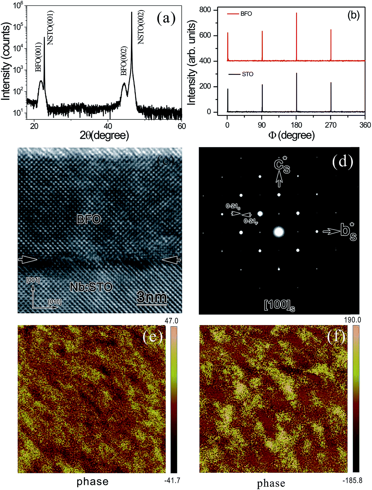 | ||
Fig. 1 (a) XRD θ–2θ scan for BFO(15 nm)/NSTO(001) film, (b) XRD ϕ scans for the reflection planes of BFO (011) and NSTO (011), (c) a high-magnification cross-sectional bright-field TEM image of BFO/NSTO(001), (d) an electron diffraction pattern from plan view sample which covers both the film and the substrate. Two big black arrows indicate the reciprocal lattice basis vectors of the substrate, and two small black arrows indicate the spiting of 0![[2 with combining macron]](https://www.rsc.org/images/entities/char_0032_0304.gif) 1 into 01S (from substrate) and 01F (from film); the subscript “F” and “S” correspond to the “Film” and the “Substrate”, respectively. (e) In plane and (f) out of plane domain structures of BFO/NSTO heterostructure at the same location with PFM image size of 2 μm × 2 μm. 1 into 01S (from substrate) and 01F (from film); the subscript “F” and “S” correspond to the “Film” and the “Substrate”, respectively. (e) In plane and (f) out of plane domain structures of BFO/NSTO heterostructure at the same location with PFM image size of 2 μm × 2 μm. | ||
Fig. 1c shows a cross-sectional bright-field TEM image of BFO/NSTO heterostructure along the NSTO [100] direction. The interface between the film and the substrate is reasonably sharp and flat, as marked by a pair of arrows. Fig. 1d is an electron diffraction pattern (EDP) taken from the area includes of both BFO film and NSTO substrate. Two basis vectors of the substrate are indicated by two big black arrows. The split of the diffraction spots is observable along the growth direction due to the lattice mismatch between the BFO film and NSTO substrate, as indicated by two small arrows. High order diffraction spots, for example 01, are split into two spots 01S (from substrate) and 01F (from film), therefore, the pseudo cubic lattice parameters of the film cF is longer than that of the substrates cS. The pseudo cubic lattice parameters of the BFO film are aF = bF = 0.3905 nm and cF ≈ 0.4054 nm, which refers to the lattice parameter of the substrate 0.3905 nm. Fig. 1e and f show the in-plane and out of plane PFM images at the same area, which indicated partial ferroelectric domain structures of BFO(15 nm)/NSTO(001) heterostructure. It is also noticed that the contrast of domain structures is small and these domains cannot be switched by applying ±10 V by PFM tip, which might possibly due to the very thin BFO films and relatively large leakage.
Fig. 2a shows the typical I–V curves of an Au/BFO/NSTO(001) structure. When the positive voltage is applied on the top (Au) electrodes, as is shown in the inset of Fig. 2a, it defines as positive bias. A current compliance 0.1 μA is applied to prevent permanent dielectric breakdown of the junction. The sweeping voltage was scanned along 1 → 2 → 3 → 4 → 1, as is denoted in Fig. 2a. Hysteretic RS behavior is observed without any electroforming process in advance. The resistance state, the high resistance state (HRS) or the low resistance state (LRS), depends on the polarity of sweeping fields, which indicates a bipolar RS. In a cycle of voltage sweeping 0 → 2 V → 0 → −6 V → 0, it corresponds to the variation of resistance states 1(HRS) → 2(LRS) → 3(LRS) → 4(HRS). Unlike filamentary-type switching in thick polycrystalline BFO by Shuai et al.19 and Chen et al.,20 the resistance switching between LRS and HRS is gradual rather than abrupt. An obvious diode-like rectifying I–V characteristic is observed at either HRS (4 and 1) or LRS (2 and 3). The rectifying ratio is about 104 measuring at ±1.5 V, which is comparable to previously reported values on junctions with thick BFO barriers.18,29 The resistance evolution are checked and read at 1 V in each dc sweep cycle, and the magnitudes of HRS and LRS are 10 MΩ and 0.1 MΩ, respectively. No significant degradation of the resistance ratio of HRS/LRS is found within measured cycles, as is shown in Fig. 2b. We also checked more than 30 Au/BFO/NSTO capacitors, and their RS behaviors performed similarly.
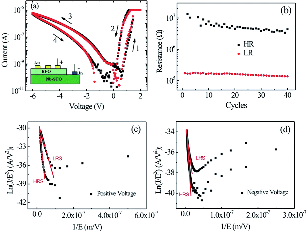 | ||
| Fig. 2 (a) I–V curves for Au/BFO/NSTO junctions. The voltage sweeps along 0 → 2 V → 0 → −6 V → 0 in a step of 50 mV and a duration delay of 0.1 s per step. The arrows indicate the sweep direction of the applied voltage. The two curves in color black and red are different cycles from the same sample. The panel of inset schematically illustrates the electrode configuration. (b) Resistance evolution of Au/BFO/NSTO junctions. The resistances of HRS and LRS were read out at a reading voltage of 1 V. 40 cycles costs about 29 minutes. ln(J/E2) vs. (1/E) plots of HRS and LRS at (c) positive voltage bias and (d) negative voltage bias. | ||
To elucidate the conductive mechanism of the Au/BFO/NSTO junction, a round cycle of I–V characteristics was fitted, as the processes 1 → 2 → 3 → 4 shown in Fig. 2a. There are four possible leakage mechanisms: the space-charge-limited current (SCLC); the bulk-limited Poole–Frenkel (PF) emission; the interface-limited Schottky emission; and the interface-limited Fowler–Nordheim (FN) tunneling.1 The first two, SCLC and PF emission, are bulk-limited conduction, which depends on the electrical properties of the dielectric film itself. The latter two, Schottky emission and FN tunneling, are interface-limited conduction, which depends on the electrical properties at the electrode–dielectric interface. It indicates that the fitting plots of ln(J/E2) − (1/E) in Fig. 2c and d are the best fitting at either positive or negative voltage, where J is current density and E is electric field. The smooth fitting of ln(J/E2) − (1/E) is a signature of interface-limited FN tunneling through a triangular potential barrier, which is very different from that in BFO thick films.19,20,30 Since Au/BFO/NSTO structure has two different interfaces, a metallic SrRuO3 (SRO 50 nm) interlayer was inserted to examine which one plays a role. The I–V curves of Au/BFO/SRO/NSTO structure shows no obvious RS behaviors and no obvious rectifying diode effect. It indicates that both of metal/BFO interfaces (Au/BFO and SRO/BFO) have no contribution to RS behavior. Therefore, we would say that the RS behavior of Au/BFO/NSTO structure is attributed to BFO/NSTO interface.
The FN tunneling current can be written as:31
 and effective mass of bulk BFO mBFO = 5 e, we have the barrier height: ϕ1 = 0.075 eV, ϕ2 = 0.032 eV, ϕ3 = 0.055 eV, and ϕ4 = 0.089 eV corresponding to the processes 1, 2, 3 and 4, respectively. The calculated barrier heights ϕ1–ϕ4 are relatively small, but they are higher than thermal energy at room temperature. For a further discussion, since the ultrathin film has weak confinement at both interfaces, it is possible that the actual value of mBFO in ultrathin film may be smaller than bulk materials (mBFO = 5 e), which might cause a higher values of barrier height.32 We also notice that, due to the relatively low energy barrier, the conductive contribution from the variation of depletion width to the dominated FN tunneling at BFO/NSTO interface cannot be neglected. The variation of depletion width will cause the change of the junction capacitance, and thus can be determined by the capacitance–voltage (C–V) measurements in Au/BFO/NSTO junctions.
Fig. 3a shows C–V measurements of the Au/BFO/NSTO junction at a frequency of 1 kHz with an AC bias of 50 mV. The capacitance at negative bias performs differently depending on the low or high resistance state of BFO film. As a result, the Au/BFO/NSTO junction shows a polarization dependent capacitance.3,19 The data of capacitance at higher positive bias (>+1 V) became noisy and unstable due to larger leakage current of Au/BFO/NSTO junction. In a conventional model of a parallel-plates condenser, the interfacial dielectric layer thickness (BFO) can be written as WD = ε0εrAeff/C, where ε0 is the permittivity of free space, εr = 11.8 is the relative dielectric constant (measured at 1 kHz), Aeff is the area of circular capacitor (with diameter 450 μm), and C is the capacitance.3 For BFO/NSTO junction, BFO film consists of the depletion layer of p–n BFO/NSTO junction and the reduced BFO layer. Since the conductivity at the reduced BFO layer is higher than that at the depletion layer, a thicker depletion layer will causes smaller capacitance or thicker WD in Au/BFO/NSTO junction. Fig. 3b shows the plots of WD as a function of applied voltage. The narrower depletion width makes it easy for electrons to pass through the barrier via a FN tunneling, which is LRS. Reversely, the thicker depletion width makes it difficult for electrons tunneling, which is HRS. We also checked the C–V measurements for the Au/BFO/SRO/NSTO(001) junction.
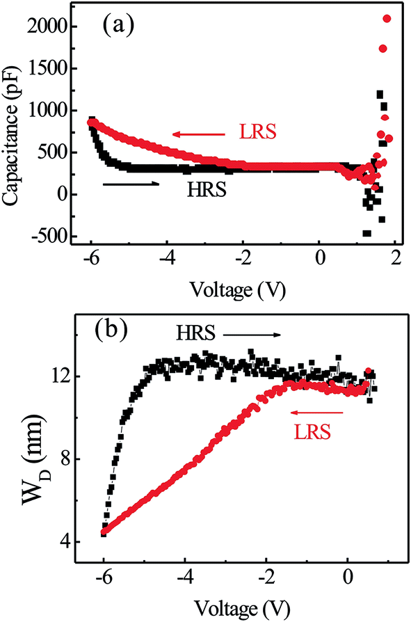 | ||
| Fig. 3 (a) C–V curves, and (b) WD–V curve of Au/BFO/Nb-STO junction at a frequency of 1 kHz with an AC bias of 50 mV. The arrows indicate the sweeping voltage, and LRS and HRS are the low and high resistance state. | ||
The partial ferroelectric domain structures in Fig. 1e and f only reveal the local static polarization behavior for ultrathin BFO film. The BFO film also shows a round hysteresis loops (not shown here) due to a relatively large leakage current at very thin film. The dynamic switching properties for BFO/NSTO heterostructure is very week, but it is still possible to be detected by the evolution of polarization flipping in Au/BFO/NSTO junctions utilizing the positive-up-negative-down (PUND) method.33,34 The experimental setup was shown in our previous paper.34 During the measurements, the BFO film was first driven to the downward polarized state (DPS) by a positive pulse (with amplitude 10 V and pulse width 12 μs) then to an intermediate state by a negative pulse with the amplitude between 0 and 10 V, seen as the applied pulse train shown in the inset of Fig. 4a. The transient current (ISW) yielded by polarization switching was measured by the voltage on an in-series resistor of 100 Ω. The switching polarization (PSW) was quantified by the area below the ISW–time (t) curve, divided by the electrode area. Fig. 4a shows the ISW–t curves for Au/BFO(15 nm)/NSTO junction, where the transient current first jumps to a peak value and then quickly decays to zero. Increasing the magnitude of pulse voltage, the current peak grows. The 2PSW of BFO film with poling voltage is presented in Fig. 4b, where PSW is the switching polarization. It indicates that the polarization of ultrathin BFO film can be switched partially(2PSW = 0.98 μC cm−2 at 10 V), even though its switching polarization is small and could not be saturated by pulsed voltage up to 10 V due to relatively large leakage current.
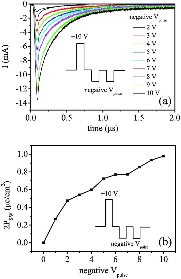 | ||
| Fig. 4 PUND measurements for Au/BFO/NSTO(100) junction. (a) Time dependence of the switching current with varied negative Vpulse. (b) 2PSW–Vpulse curve derived from the transient current. | ||
Based on our detailed experimental results, the observed RS behavior of Au/BFO/NSTO junction can be attributed to the interfacial effect at BFO/NSTO interface, and it can be qualitatively interpreted by the ferroelectric polarization modulation of the Schottky barrier height and variation of depletion width at BFO/NSTO interface.35–37
Fig. 5a shows the energy band diagram of isolated Au, BFO and NSTO layers. The electron affinity and energy band gap are 3.3 eV and 2.8 eV for BFO,9 and 3.2 eV and 4 eV for NSTO,38,39 respectively. Since NSTO can be considered as a non-degenerate semiconductor, its Fermi level EF lies ∼3 kT below the conductive band EC.29 For BFO thin film, because of the volatility of Bi during deposition, there is usually a sizable amount of Bi vacancies. BFO with Bi vacancies could be considered as a p-type semiconductor.29,40 Therefore, the work function of BFO and NSTO will be (4.7 − x) eV and (4.08 + y) eV, respectively, where x and y are small numbers. As a result of the inter-diffusion of majority carriers (electrons) from NSTO into BFO, a depletion layer forms p–n junction at the BFO/NSTO interface. If there is no external influence, the depletion width will be at a certain degree when reaching the dynamic equilibrium. Fig. 5b and c schematically show the distribution of space charges in depletion region at LRS and HRS, respectively. When the ferroelectric polarization of BFO film is downward (positive), the polarization bound charges repel the electrons backwards to NSTO, which results in a reducing of the depletion width at the BFO/NSTO interface, as is shown in Fig. 5b. In contrast, when the polarity of ferroelectric polarization in BFO layer is reversed (upward) by applying a large negative voltage, the electrons in NSTO layer are attracted by the polarization bound charges at the BFO film, resulting in an increase of the depletion width, as shown in Fig. 5c.
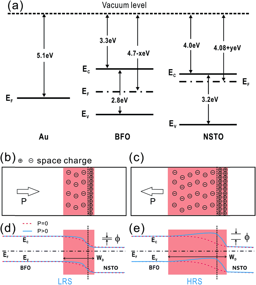 | ||
| Fig. 5 (a) Diagram of energy bands for isolated Au, BFO and NSTO layers; (b and c) charge distribution of depletion region at the BFO/NSTO interface for LRS and HRS, and (d and e) energy band diagram at the BFO/NSTO interface for LRS and HRS. | ||
The depletion layer causes an energy band bending which leads to the variation of the potential barrier height at the BFO/NSTO interface. The interface barrier height ϕ is composed of build-in barrier ϕbuild-in and the interface barrier ΔϕP induced by the depolarization field at the depletion region,18,41 i.e., ϕ = ϕbuild-in + ΔϕP. The build-in barrier ϕbuild-in = ϕS(BFO) − ϕS(NSTO) − [χ(BFO) − χ(NSTO)] = (1.32 − x − y) eV, where ϕS and χ are work function and affinity energy, respectively. The potential barrier height ϕ is modulated by the ferroelectric polarization in BFO layer. Fig. 5d and e show the schematic energy diagram at LRS and HRS, respectively. For the downward ferroelectric polarization, the narrower depletion layer results a lower interface barrier ΔϕP, as is shown in Fig. 5b and d. For the upward ferroelectric polarization, reversely, the wider depletion layer results a higher interface barrier ΔϕP, as shown in Fig. 5c and e.
Based on our experimental results, the resistance switching behaviors (LHR and HRS) can be mainly attributed to the ferroelectric polarization modulation of the depletion width and potential barrier height at the BFO/NSTO interface, and we cannot exclude the effect of defects, e.g. oxygen vacancy, at BFO/NSTO interface. When the polarization is downward by applying a large positive voltage, for example the process of 2 (or 3) in Fig. 2a, the BFO/NSTO interface has narrower depletion width and lower energy barrier ϕ2 (or ϕ3), which makes it easy for electrons tunneling through the BFO/NSTO interface, which results in a low resistance state. Reversely, when the polarity of polarization is reversed (upward) in the process of 4 (or 1) in Fig. 2a, the BFO/NSTO interface has wider depletion width and higher energy barrier ϕ4 (or ϕ1), which makes it difficult for electrons tunneling through the BFO/NSTO interface, which results in a high resistance state.
IV. Conclusions
In summary, just the interfacial effect on resistance switching in Au/BFO/NSTO junction was presented. I–V characteristic indicates diode-like effect and RS behavior in Au/BFO/NSTO(001) junction. The on/off resistance ratio at +1 V is about two orders of magnitude. The conductive mechanism is dominated by the interface-limited Fowler–Nordheim (FN) tunneling through a triangular potential barrier formed at BFO/NSTO interface. The switching polarization dynamics indicates that BFO film is ferroelectric with weak polarization. The C–V curve provides direct evidence of the variation of the depletion width at the Au/BFO/NSTO interface. The resistance switching behaviors can be attributed to the ferroelectric polarization modulation of the energy barrier height and depletion width at the BFO/NSTO interface.Acknowledgements
The authors gratefully acknowledge the supports of the State Key Project of Fundamental research of China under Grants No. 2015CB921402, National Natural Science Foundation of China No. 11374189, 51231007, and 11627805, 111 Project B13029, and China electronics technology group corporation No. 46 research institute No. CJ20130304.References
- D. S. Jeong, R. Thomas, R. S. Katiyar, J. F. Scott, H. Kohlstedt, A. Petraru and C. S. Hwang, Rep. Prog. Phys., 2012, 75, 076502 CrossRef PubMed.
- A. Sawa, Mater. Today, 2008, 11, 28–36 CrossRef CAS.
- R. Waser, Nat. Mater., 2007, 6, 833–840 CrossRef CAS PubMed.
- A. Q. Jiang, C. Wang, K. J. Jin, X. B. Liu, J. F. Scott, C. S. Hwang, T. A. Tang, H. B. Lu and G. Z. Yang, Adv. Mater., 2011, 23, 1277–1281 CrossRef CAS PubMed.
- A. Asmitsu, Y. Tomioka, H. Kuwahara and Y. Tokura, Nature, 1997, 388, 50–52 CrossRef.
- J. Borghetti, G. S. Snider, P. J. Kuekes, J. J. Yang, D. R. Stewart and R. S. Williams, Nature, 2010, 464, 873–876 CrossRef CAS PubMed.
- T. W. Kim, D. F. Zeigler, Q. Acton, H. L. Yip, H. Ma and A. K. Y. Jen, Adv. Mater., 2012, 24, 828–833 CrossRef CAS PubMed.
- R. Meyer, J. Appl. Phys., 2006, 100, 051611 CrossRef.
- M. Dawber, K. M. Rabe and J. F. Scott, Rev. Mod. Phys., 2005, 77, 1083–1130 CrossRef CAS.
- J. J. Yang, M. D. Pickett, X. Li, D. A. Ohlberg, D. R. Stewart and R. S. Williams, Nat. Nanotechnol., 2008, 3, 429–433 CrossRef CAS PubMed.
- S. H. Jo, K. H. Kim and W. Lu, Nano Lett., 2009, 9, 870–874 CrossRef CAS PubMed.
- T. Zhao, A. Scholl, F. Zavaliche, K. Lee, M. Barry, A. Doran, M. P. Cruz, Y. H. Chu, C. Ederer, N. A. Spaldin, R. R. Das, D. M. Kim, S. H. Baek, C. B. Eom and R. Ramesh, Nat. Mater., 2006, 5, 823–829 CrossRef CAS PubMed.
- T. Choi, S. Lee, Y. J. Choi, V. Kiryukhin and S. W. Cheong, Science, 2009, 324, 63–66 CrossRef CAS PubMed.
- S. Y. Yang, J. Seidel, S. J. Byrnes, P. Shafer, C. H. Yang, M. D. Rossell, P. Yu, Y. H. Chu, J. F. Scott, J. W. Ager, L. W. Martin and R. Ramesh, Nat. Nanotechnol., 2010, 5, 143–147 CrossRef CAS PubMed.
- R. Palai, R. S. Katiyar, H. Schmid, P. Tissot, S. J. Clark, J. Robertson, S. A. T. Redfern, G. Catalan and J. F. Scott, Phys. Rev. B: Condens. Matter Mater. Phys., 2008, 77, 014110 CrossRef.
- C. H. Yang, J. Seidel, S. Y. Kim, P. B. Rossen, P. Yu, M. Gajek, Y. H. Chu, L. W. Martin, M. B. Holcomb, Q. He, P. Maksymovych, N. Balke, S. V. Kalinin, A. P. Baddorf, S. R. Basu, M. L. Scullin and R. Ramesh, Nat. Mater., 2009, 8, 485–493 CrossRef CAS PubMed.
- A. Tsurumaki, H. Yamada and A. Sawa, Adv. Funct. Mater., 2012, 22, 1040 CrossRef CAS.
- T. L. Qu, Y. G. Zhao, D. Xie, J. P. Shi, Q. P. Chen and T. L. Ren, Appl. Phys. Lett., 2012, 98, 173507 CrossRef.
- Y. Shuai, S. Q. Zhou, D. Bürger and M. Helm, J. Appl. Phys., 2011, 109, 124117 CrossRef.
- X. M. Chen, G. H. Wu, H. L. Zhang, N. Qin, T. Wang, F. F. Wang, W. Z. Shi and D. H. Bao, Appl. Phys. A, 2011, 100, 987–990 CrossRef.
- Y. P. Guo, B. Guo, W. Dong, H. Li and H. Z. Liu, Nanotechnology, 2013, 24, 275201 CrossRef PubMed.
- L. Feng, S. W. Yang, Y. Lin, D. L. Zhang, W. C. Huang, W. B. Zhao, Y. W. Yin, S. N. Dong and X. G. Li, ACS Appl. Mater. Interfaces, 2015, 7, 26036 CAS.
- S. Hong, T. Choi, J. H. Jeon, Y. Kim, H. Lee, H. Y. Joo, I. Hwang, J. S. Kim, S. O. Kang, S. V. Kalinin and B. H. Park, Adv. Mater., 2013, 25, 2339–2343 CrossRef CAS PubMed.
- A. Rana, H. Lu, K. Bogle, Q. Zhang, R. Vasudevan, V. Thakare, A. Gruverman, S. Ogale and N. Valanoor, Adv. Funct. Mater., 2014, 24, 3962–3969 CrossRef CAS.
- K. Yin, M. Li, Y. Liu, C. He, F. Zhuge, B. Chen, W. Lu, X. Pan and R. W. Li, Appl. Phys. Lett., 2010, 97, 042101 CrossRef.
- W. Shen, A. Bell, S. Karimi and I. M. Reaney, Appl. Phys. Lett., 2012, 100, 133505 CrossRef.
- L. Wu, C. Jiang and D. Xue, J. Appl. Phys., 2014, 115, 17D716 CrossRef.
- H. Béa, M. Bibes, S. Petit, J. Kreisel and A. Barthélémy, Philos. Mag. Lett., 2007, 87, 165–174 CrossRef.
- H. Yang, H. M. Luo, H. Wang, I. O. Usov, N. A. Suvorova, M. Jain, D. M. Feldmann, P. C. Dowden, R. F. Depaula and Q. X. Jia, Appl. Phys. Lett., 2008, 92, 102113 CrossRef.
- H. Yang, M. Jain, N. A. Suvorova, H. Zhou, H. M. Luo, D. M. Feldmann, P. C. Dowden, R. F. DePaula, S. R. Foltyn and Q. X. Jia, Appl. Phys. Lett., 2007, 91, 072911 CrossRef.
- R. H. Fowler and L. W. Nordheim, Proc. R. Soc. London, Ser. A, 1928, 119, 173–181 CrossRef CAS.
- P. Pipinys, A. Rimeika and V. Lapeika, Ferroelectrics, 2010, 396, 60–66 CrossRef CAS.
- J. F. Scott, L. Kammerdiner, M. Parris, S. Traynor, V. Ottenbacher, A. Shawabker and W. F. Oliver, J. Appl. Phys., 1988, 64, 787 CrossRef CAS.
- R. L. Gao, Y. S. Shen, J. R. Sun, Y. G. Zhao, J. B. Li and B. G. Shen, Appl. Phys. Lett., 2012, 101, 152901 CrossRef.
- V. Garcia, S. Fusil, K. Bouzehouane, S. Enouz-Vedrenne, N. D. Mathur, A. Barthélémy and M. Bibes, Nature, 2009, 460, 81–84 CrossRef CAS PubMed.
- J. P. Velev, C. G. Duan, J. D. Burton, A. Smogunov, M. K. Niranjan, E. Tosatti, S. S. Jaswal and E. Y. Tsymbal, Nano Lett., 2009, 9, 427–432 CrossRef CAS PubMed.
- Z. Hu, Q. Li, M. Li, Q. Wang, Y. Zhu, X. Liu, X. Zhao, Y. Liu and S. Dong, Appl. Phys. Lett., 2012, 102, 102901 CrossRef.
- Y. Watanabe, Phys. Rev. B: Condens. Matter Mater. Phys., 1999, 59, 11257 CrossRef CAS.
- S. M. Guo, Y. G. Zhao, C. M. Xiong and P. L. Lang, Appl. Phys. Lett., 2006, 89, 223506 CrossRef.
- L. N. Zhao, Z. X. Lu, F. Y. Zhang, G. Tian, X. Song, Z. W. Li, K. P. Huang, Z. Zhang, M. H. Qin, S. J. Wu, X. B. Lu, M. Zeng, X. S. Gao, J. Y. Dai and J. M. Liu, Sci. Rep., 2015, 5, 9680 CrossRef CAS PubMed.
- J. Junquera and P. Ghosez, Nature, 2003, 422, 506–509 CrossRef CAS PubMed.
Footnotes |
| † Electronic supplementary information (ESI) available. See DOI: 10.1039/c7ra02339a |
| ‡ Present addresses: Peter Grünberg Research Center, Nanjing University of Posts and Telecommunications, Nanjing 210003, China. |
| This journal is © The Royal Society of Chemistry 2017 |