
 Open Access Article
 This Open Access Article is licensed under a Creative Commons Attribution-Non Commercial 3.0 Unported Licence
Effects of the degradation of methane sulfonic acid electrolyte on the collapse failure of Sn–Ag alloy solders for flip-chip interconnections
Mi-Seok Park ab,
Do-Hwan Nam*a,
Ki-Min Junga,
Kyung-Sik Honga and
Hyuk-Sang Kwon*a
ab,
Do-Hwan Nam*a,
Ki-Min Junga,
Kyung-Sik Honga and
Hyuk-Sang Kwon*a
aDept. of Materials Science and Engineering, Korea Advanced Institute of Science and Technology (KAIST), Daejeon 305-701, Republic of Korea. E-mail: dhnam@kaist.ac.kr; hskwon@kaist.ac.kr
bThin Film Technology Team, Samsung Electronics, Hwasung-City, 445-701, Republic of Korea
First published on 27th April 2017
Abstract
The present study investigates the degradation mechanism of a methanesulfonic acid (MSA) based electroplating bath used for the electrodeposition of Sn–Ag alloy solder bumps, and its effects on the microstructure of the solder and on the collapse failure of flip-chip solder bumps. To examine the degradation behavior of the electroplating bath, a degraded electrolyte is prepared by accelerated aging treatment. In the presence of dissolved oxygen and Ag+ ions in the electrolyte, the chemical oxidation of Sn2+ ions to Sn4+ ions and the precipitation of SnO2 nanoparticles with a diameter below 100 nm are promoted by the reduction of Ag+. Under cathodic bias, colloidal SnO2 particles are adsorbed on the surface of the Sn–Ag solder bumps via electrophoresis, and incorporated into the layer by the electrodeposition layer of Sn–Ag. The presence of oxide layer mainly composed of SnO2 on the surface of the bumps significantly reduces the friction coefficient of the solder surface by hardening the electrodeposits and deteriorates the solderability of the solder bumps, which leads to collapse failure during solder reflow.
Introduction
Flip-chip packaging has been widely used in the integrated circuit (IC) packaging industry for a long time due to its small form factor, and simple and low-cost process.1–3 Recently, as electronic devices have become smaller, thinner and lighter, solder capped Cu pillar bumping technology has been considered as the most effective method for fine-pitch connection, because the Cu pillar allows finer pitches and provides a rigid stand-off between the die and substrate, which allows better underfill in comparison to conventional solder bump technology.4–6Among lead-free solder alloys, in the past decade Sn–Ag alloy has been applied to flip-chip interconnections as a standard process in wafer-level packaging (WLP) due to its excellent creep resistance, desirable melting point, thermo-mechanical fatigue behavior, good wettability7 and greater connection reliability.8,9 The Sn–Ag alloy solder bump is commonly prepared from methanesulfonic acid (MSA) based electroplating baths which have many beneficial properties including high salt solubility, high electrolytic conductivity and the ability to dissolve many metals, which enables co-electrodeposition.10–14 However, one of the most serious issues when using the MSA based electroplating bath is that the electrolyte gradually degrades with time, particularly when it is used for mass production in industrial fields, although the composition can be maintained by adding undegraded additives and inorganic components. Because the mechanical and electrical reliability of the Sn based alloy solders are highly dependent on the electroplating conditions,15–21 the degradation of the electroplating bath leads to packaging problems.1,3,22,23 Indeed, issues such as the collapse of solder bumps during solder reflow and the non-wetting phenomena of solder surfaces with the base metal can be observed more frequently as the electroplating bath solution approaches the end of its lifetime.2,24 The collapse of the solder bumps leads to a non-contact failure, or a critical bridging failure between neighboring bumps, which results in enormous product loss and an increase in production costs. Despite this, the direct correlation between the collapsing failures and the degradation of the electroplating bath has not yet been studied.
Therefore, in this work, we investigated the degradation mechanism of the MSA based electroplating bath used for Sn–Ag alloy electrodeposition. Since the electroplating bath for Sn–Ag alloy contains several types of organic additives and two or more dissolved metal salts in the background electrolyte solution,10,25 we first examined the degradation behavior of the electrolytes before and after accelerated aging to mimic the effects of long term operation, and then the effects of the degradation of the electrolyte on the properties of the Sn–Ag solder were investigated. Lastly, a correlation between the collapsing failure of the Sn–Ag alloy solder and the degradation mechanism of the electroplating bath was suggested based on the results.
Experimental
To fabricate Sn–2.3Ag (wt%) alloy solder capped copper pillar bumps, a photo resist (PR) pattern with via hole arrays was fabricated using a conventional industrial photolithography process and mass production tools.1 The electrodeposition of the Sn–Ag alloy was carried out on the Cu stud substrate at a current density of −20 mA cm−2 for 600 s in a bath containing 2.0 mol L−1 MSA (CH3SO3H, Sigma-Aldrich), 0.192 mol L−1 tin methanesulfonate ((CH3SO3)2Sn, Sigma-Aldrich) and 0.008 mol L−1 silver methanesulfonate ((CH3SO3)Ag, Sigma-Aldrich). In addition to the basic MSA bath, 120 mL L−1 TS-SLG and 0.005 mol L−1 catechol (C6H6O2) were added as an Ag complexing agent and anti-oxidant, respectively. The electrodeposition of the Sn–Ag alloy solder was conducted using a two-electrode cell: a Sn plate was used as the anode and a silicon wafer covered with Cu seed and PR via hole patterns (illustrated in Fig. 1) was used as the cathode. All the electrodepositions were conducted at room temperature, 296 K.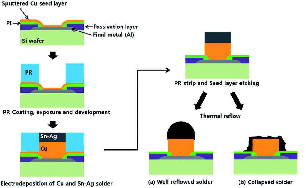 | ||
| Fig. 1 Schematic illustration of the Cu pillar bump fabrication process; (a) well reflowed solder bump and (b) collapsed solder bump during thermal reflow. | ||
After the electrodeposition of the Sn–Ag alloy on the Cu pillar, standard PR stripping and etching of the Cu seed layer were performed.1 The whole fabrication process for the solder capped Cu pillar bump is schematically illustrated in Fig. 1.
The thermal reflow of the solder was performed under standard reflow conditions with flux treatment, in compliance with the JEDEC (Joint Electronic Devices Engineering Council) requirements. The reflow profile consisted of a pre-heating range of 150–200 °C for 90 s followed by holding above 240 °C for 20 s at a peak temperature of 250 °C.
To examine the degradation behavior of the electroplating bath, we prepared a degraded bath by accelerated aging treatment. Since dissolved oxygen in the solution is considered to be the major reason for the degradation of the bath, a steady flow of air was injected into the solution at 200 mL min−1 with continuous stirring at 300 rpm for 3 weeks. Discoloration of the electroplating bath induced by the degradation of the solution was observed with a spectrophotometer (UV-3101PC, Shimadzu), which measures the light wave transmissions of the bath at different wavelengths of incident light.
To elucidate the mechanism of co-deposition of precipitated stannic oxides into the solder layer, the zeta potential of the precipitated particles were measured in a diluted solution at 25 °C using a Zetasizer Nano-ZS zeta-potential analyzer (Malvern Instruments Ltd.).
The surface morphology and microstructure of the Sn–Ag alloy were examined by scanning electron microscopy (SEM) combined with energy dispersive X-ray spectroscopy (EDS) and Cs corrected high-resolution transmission electron microscopy (HRTEM), respectively.
The phases of the colloidal particles formed on the surface of the electrodeposit were investigated using selected-area-electron-diffraction (SAED) and fast Fourier transformation (FFT) analysis. The crystal structures and chemical composition of the sludge formed by the accelerated aging tests were characterized by X-ray diffraction (XRD).
To investigate the mechanical properties of the solder bump, the tribological behaviors of the solder films formed by an undegraded electroplating bath or degraded bath were examined using dry sliding friction and wear tests. The solder plated samples were reciprocated at a constant speed of 2 Hz (0.6 mm s−1) against a 1.0 mm diameter ceramic silicon nitride (Si3N4) ball (the counter-body). Contact loads of 20 mN were applied. To estimate the wear rate, the wear track was measured by laser scanning confocal microscope (VK-250, KEYENCE). To examine the effect of the bath degradation on the hardness of the electrodeposits, Vickers microhardness indentation tests were performed on the solder samples using a micro-hardness tester (HM-124, Mitutoyo) at the indentation load of 40 mN with a holding time of 5 s. After load removal, diagonals of the indentation were measured with an optical microscope and an automatic indentation detection program (VLPAK2000, Mitutoyo).
Results and discussion
Fig. 2 shows the surface morphologies of the Sn–2.3Ag alloy solder bumps electrodeposited from two different baths, which had been used in the mass-production electroplating process for one week, and three weeks, respectively. The inset images of Fig. 2a and b show the color changes of the solution with time. Typical electroplating baths that contain MSA, tin methanesulfonate, silver methanesulfonate, TS-SLG and catechol are transparent and colorless, but the color of the solution changed to light-yellow after using it for one week, and to muddy gray after using it for three weeks in mass production.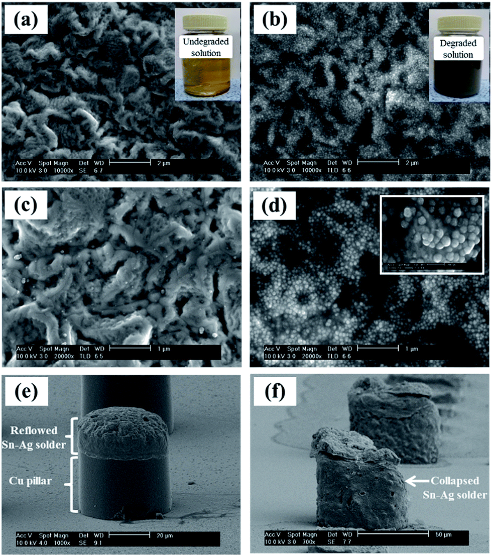 | ||
| Fig. 2 The surface morphology of the Sn–Ag alloy bumps electrodeposited from ((a) and (c)) the undegraded bath and ((b) and (d)) the degraded solution. The insets of (a) and (b) are the photos of the undegraded and degraded solution, respectively. Thermal reflowed Sn–Ag solder bumps electrodeposited from (e) the undegraded bath and (f) the degraded solution. | ||
When the Sn–Ag alloy bumps were electrodeposited on Cu pillars from the lite-yellow solution (which had been used for one week), well reflowed Sn–Ag solders could be prepared, as shown in Fig. 2e. The overall morphology of the Sn–Ag alloy bumps electrodeposited from the gray solution (used for three weeks) looked similar to those from the one-week old solution. However, high-magnification SEM images (Fig. 2c and d) reveal that a Sn–Ag alloy bump electrodeposited from the three-week old solution was fully covered with spherical particles which have diameters ranging between 50 nm and 100 nm, whereas there were no nanoparticles on the bump electrodeposited from the one-week old solution. In particular, the bumps from the three-week old solution completely collapsed and debris was scattered around the Cu pillar bumps after the thermal reflow process (Fig. 2f), which is totally different behavior from that observed in Fig. 2e. Therefore, the results clearly show that the degradation of the electrolyte not only affects the surface morphology of the Sn–Ag bumps, but also leads to the collapse failure of solder bumps during the solder reflow step.
In addition to morphological changes, the mechanical properties of the solder bumps were also significantly affected by the degradation of the bath. Fig. 3 presents the results of the microscale friction, wear and hardness tests for the Sn–Ag alloy bumps prepared from solutions before and after degradation. As the bath was degraded, the coefficients of friction (COF) vs. sliding time curves show different tribological behavior (Fig. 3a). The frictional response of the sample formed from the undegraded bath showed an initial COF value of 0.5, and this value settled to 0.75 after 200 s. In contrast, the COF of the sample formed from the degraded bath was 0.2, and this value settled to 0.55 after 450 s. The tribological performance suggests that the degradation of the electrolyte can reduce the friction coefficient of the solder surface by hardening the electrodeposits. As shown in Fig. 3b and c, the wear scar on the surface of the Sn–Ag electrodeposits prepared from the degraded solution was broader and deeper (0.414 mm3) than that of the electrodeposits prepared from the undegraded solution (0.084 mm3). Moreover, as shown in Fig. 3d, the hardness of the sample formed from the degraded bath shows the greater hardness value of 50.6 by HV0.002 (Fig. 3f) than the hardness value of the sample formed from the undegraded bath (24.7 by HV0.002 (Fig. 3e)). These tribological behaviors and the hardening effects are consistent with previous reports26–28 that discussed the correlation between surface micro-hardness and the surface frictional property. Because the mechanical properties and the melting temperature of solder alloy are highly dependent on the microstructure and the composition of the solder alloy,29–31 these results suggest that the degradation of the bath has a negative influence on the fabrication of solder bumps. The formation of nanoparticles on the Sn–Ag solder bumps therefore may be one of the major causes of the collapse of the solder bumps during the solder reflow shown in Fig. 2f.
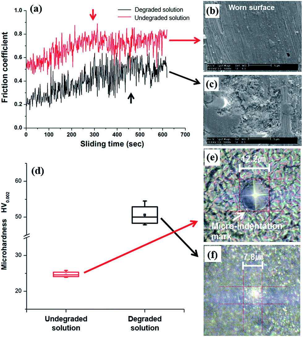 | ||
| Fig. 3 (a) Plot of friction coefficient vs. sliding time for two samples slid at a normal load of 20 mN. SEM images of the worn surface of the solders formed from (b) the undegraded bath and (c) degraded bath. (d) The Vickers microhardness values of the samples. Optical micrographs of Vickers indentation (40 mN) on the solders formed from (e) the undegraded bath and (f) degraded bath. | ||
To analyze the nanoparticles formed on the surface of the bumps, the Sn–Ag alloy electrodeposits prepared from the degraded solution were further examined using TEM. The cross-sectional TEM image confirms the presence of the nanoparticles on the surface of the Sn–Ag alloy solder (Fig. 4a), in accordance with the SEM observation (Fig. 2d). In addition, a number of nanoparticles were also observed embedded in the subsurface layer as well as on the top surface of the solder bump (Fig. 4b). As shown in Fig. 4c, the SAED pattern for these nanoparticles shows the clear ring patterns of a polycrystalline structure, which are attributed to the (110), (101) and (211) planes of SnO2. One notable feature in the HRTEM observation is that a native oxide layer was observed at the interface between the SnO2 particles and the surface of the Sn–Ag electrodeposits (Fig. 4c). The meniscus shape of the native oxide implies that the SnO2 particles were probably not acquired during the post electrodeposition process, but rather formed on the surface of the solder layer during the electrodeposition process.
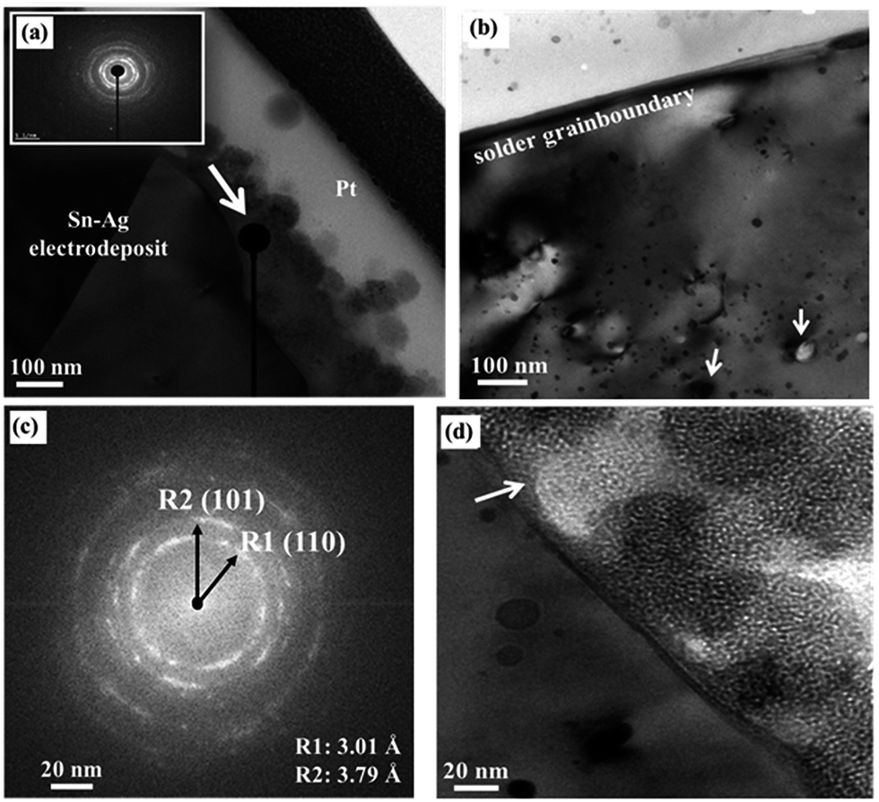 | ||
| Fig. 4 (a and b) Cross-sectional TEM images and (c) SAED pattern of Sn–Ag alloy solder formed by the degraded electroplating bath showing the deposition of SnO2 nanoparticles on the surface of the Sn–Ag electrodeposit. (d) The native oxide layer with the meniscus curved shape formed at the interface between SnO2 nanoparticles and Sn–Ag alloy solder. | ||
To reveal their exact chemical compositions, XPS analysis was performed on the electrodeposited solder formed by the degraded solution. As shown in Fig. 5, the XPS spectra show the single peak curves of the surface (without ion etching) and double peak curves of the subsurface (after ion etching for 300 s and more). This indicates that Sn4+ was the dominant species on the top surface, but the subsurface was composed of Sn, Sn2+ and Sn4+. Since the Sn2+ and Sn4+ spectra are still substantial at the deep subsurface exposed by ion beam etching for 540 s, it can be deduced that the deep subsurface and the top surface of the solder formed from the degraded bath were substantially composed of stannous and stannic oxide. According to a previous report,32,33 an oxidation layer with a thickness of less than a few tens of nanometers formed on the Sn–based solder surface can significantly affect its solderability due to the non-wetting behavior between the solder bump and solder on the pad substrate. In this respect, the existence of a thick oxide layer mainly composed of SnO2 nanoparticles (tens of nm) is expected to degrade the solder wetting property18 and lead to failures, such as the collapse of the solder bumps during the solder reflow.
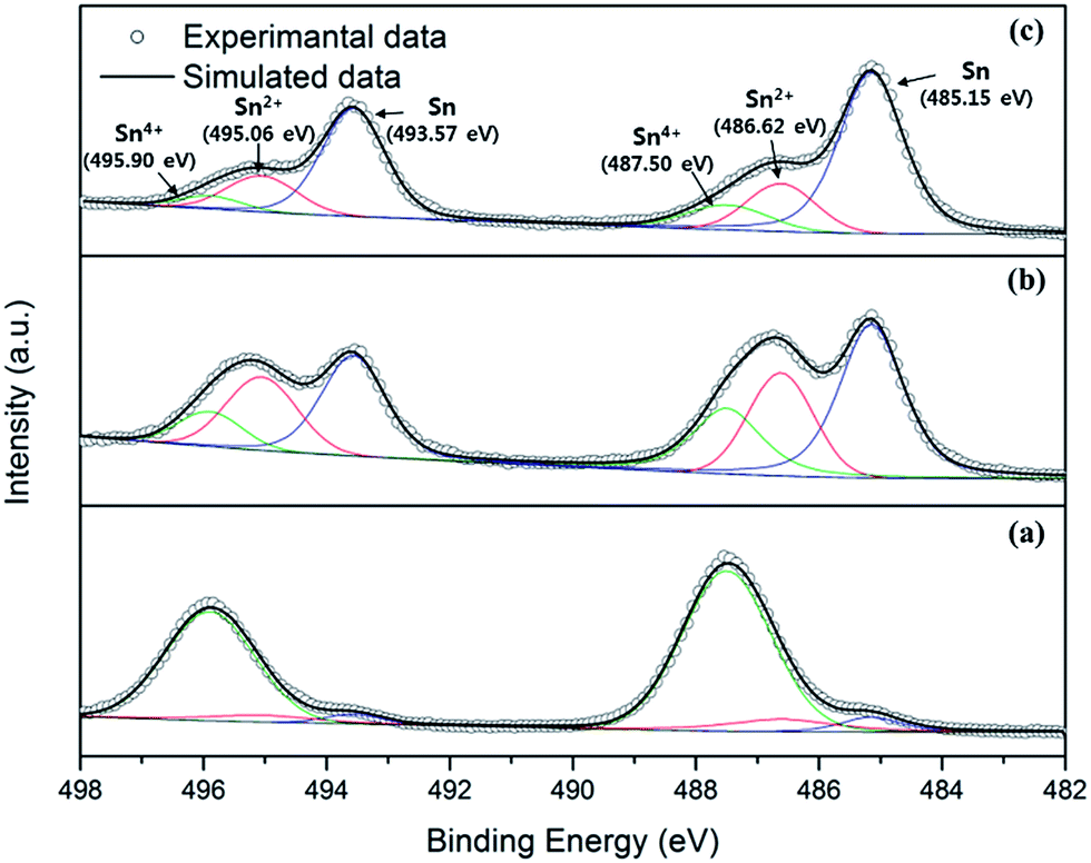 | ||
| Fig. 5 Sn 3d XPS spectra of the electrodeposited film covered with spherical particles obtained from the degraded bath: (a) w/o ion etching, (b) with ion etching for 300 s and (c) with ion etching for 540 s. | ||
To understand the formation and deposition mechanisms of the SnO2 nanoparticles on the surface of the Sn–Ag bump, an accelerated degradation experiment was performed. To mimic the harsh conditions of the mass production environment, a compulsory aeration and agitation process was carried out on the MSA based electroplating solution.
As shown in Fig. 6b and c, when Ag ions coexist in the Sn–MSA bath (solution II), the color changes are more obvious and much faster than in the Ag-free bath (solution I). While the color of solution I changed to a light yellow, the color of sample II changed to dark gray after three weeks, followed by the precipitation of a gray colored sludge. The transmittance of visible light at 450 nm through the degraded solution II decreased to below 30% after 3 weeks, whereas solution I retained ∼60% of its transmittance (Fig. 6d).
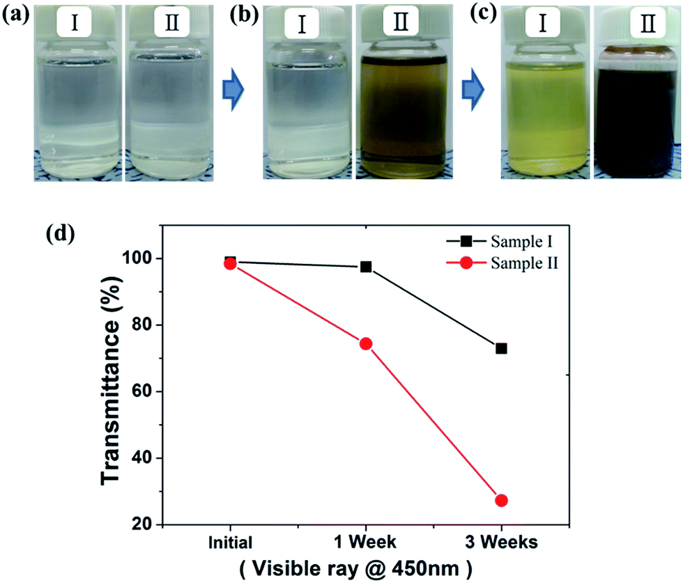 | ||
| Fig. 6 The color changes of (I) the Sn–MSA solution and (II) Sn–MSA with Ag cations (a) as prepared, (b) after a week and (c) after 3 weeks. (d) The transmittance of a visible ray at 450 nm wavelength for the solutions with time. | ||
To analyze the species that precipitated after degradation, sludge particles were obtained by centrifugal separation. As shown in Fig. 7, the morphology and size of the particles were similar to the SnO2 nanoparticles deposited on the surface of the Sn–Ag bumps (Fig. 2d). In addition, all of the peaks in the diffraction pattern of the sludge particles matched that of crystalline SnO2 (JCPDS no. 77-0450). Therefore, it can be assumed that the SnO2 nanoparticles observed on the surface of the Sn–Ag bumps are formed in the solution through spontaneous chemical reactions, not during the electrodeposition.
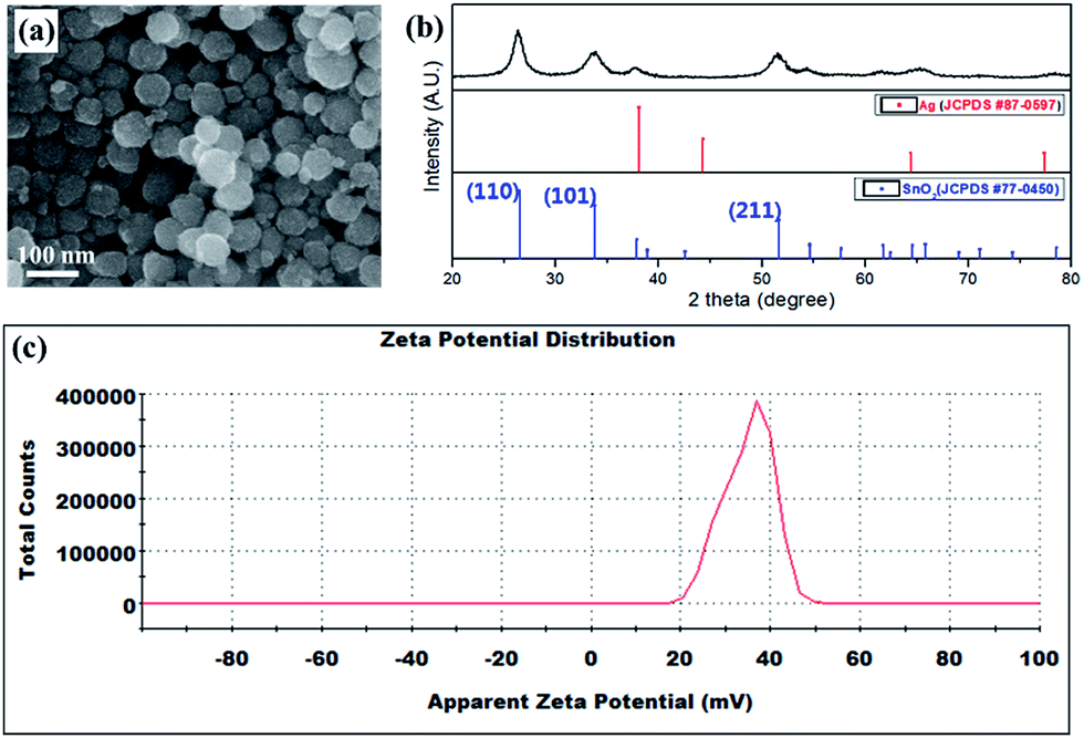 | ||
| Fig. 7 (a) SEM image and (b) XRD pattern for the precipitated SnO2 particles extracted from sample II shown in Fig. 6(c). (c) A surface zeta potential graph of SnO2 particles precipitated from the degraded bath (pH 1.8). | ||
The following reactions (1)–(3) are the possible reaction routes of Sn2+ oxidation and SnO2 precipitation with dissolved oxygen in an aqueous solution containing metastannic acid (H2SnO3).20,34
| 2Sn2+ + O2 + 4H+ → 2Sn4+ + 2H2O | (1) |
| Sn4+ + 4H2O → Sn(OH)4 + 4H+ | (2) |
| Sn(OH)4 → H2O + H2SnO3↓(→ 2H2O + SnO2 (s)↓) | (3) |
However, since the amount of the precipitated SnO2 particles in solution II was much larger than the solution I, it is likely that the Ag+ ions dissociated from the methanesulfonate complex promotes the oxidation of stannous ions to stannic ions, and the precipitation of SnO2 particles is produced by the reduction of metallic silver (Ag0) by the following reaction (4).20
| Sn2+ + 2Ag+ (aq) → Sn4+ + 2Ag (s) | (4) |
Fig. 7c shows that the zeta potential of the precipitated SnO2 particles in the degraded bath is about 35.1 mV. The result indicates that the surfaces of the SnO2 particles are positively charged in the degraded bath (pH 1.8), which is consistent with a previous study that SnO2 particles have positive zeta potentials in the pH range below 4.3, and negative values at pH higher than 4.3 (i.e., the isoelectric point of SnO2 is about pH 4.3).35,36
During the electrodeposition of the Sn–Ag alloy, the application of an electric field induces a coulombic force on the SnO2 particles, and thus positively charged SnO2 particles approach the negatively charged working electrode. This phenomenon is the well-known phenomenon of electrophoresis.37 Therefore, it can be assumed that the electrophoretic deposition of SnO2 nanoparticles occurs simultaneously with the electrodeposition of Sn–Ag alloy, which results in the incorporation of nanoparticles into the subsurface layer as well as the deposition on the top surface of the solder bump (Fig. 4b).
Conclusions
In summary, the degradation mechanism of the MSA based electroplating bath used for Sn–Ag alloy electrodeposition was investigated, with emphasis on the effects of the solution degradation on the morphological and mechanical properties of the Sn–Ag bumps. SEM and TEM observations revealed that SnO2 nanoparticles were deposited on the surface of the bumps during the electrodeposition of Sn–Ag alloy, which led to the collapse failure of the solder bumps during solder reflow. In addition to morphological changes, the microscale friction, wear and hardness tests demonstrated that the solution degradation can reduce the friction coefficient of the solder surface by hardening the electrodeposits, which has a negative influence on the fabrication of solder bumps.From the accelerated degradation experiment, it was found that the formation of SnO2 nanoparticles was not due to an electrochemical reaction, but could be attributed to the chemical oxidation of Sn2+ to Sn4+. Notably, the dissolved oxygen in the solution was the dominant factor leading to the degradation of the solution, but the results demonstrated that the coexistence of Ag+ in the solution significantly promoted the oxidation of Sn2+ ions, and the precipitation of SnO2 particles. In the presence of Ag+ the precipitated SnO2 particles were adsorbed on the surface of the Sn–Ag solder bumps via electrophoresis, and incorporated into the layer during electrodeposition. The formation of a thick oxide layer mainly composed of SnO2 nanoparticles on the surface of bumps deteriorates the solderability of the solder bumps and leads to collapse failures during the solder reflow.
The present work suggested for the first time a correlation between the degradation of the MSA based electroplating bath for Sn–Ag alloy and the collapse failure of the Sn–2.3Ag solder bump. We believe that the degradation mechanism and analysis techniques reported in this study provide a facile way to investigate and predict the degradation of the electroplating bath during the mass production of Sn–Ag bumps.
Acknowledgements
This work was supported by the BK21PLUS program through the National Research Foundation (NRF) of Korea [Grant numbers 2015-074668]. This work was also funded by Samsung Electronics Co. Ltd.Notes and references
- M. Datta, Electrochemical processing technologies in chip fabrication: challenges and opportunities, Electrochim. Acta, 2003, 48, 2975 CrossRef CAS.
- K. Zeng and K. N. Tu, Six cases of reliability study of Pb-free solder joints in electronic packaging technology, Mater. Sci. Eng., R, 2002, 38, 55 CrossRef.
- K. N. Tu, Recent advances on electromigration in very-large-scale-integration of interconnects, J. Appl. Phys., 2003, 94, 55 CrossRef.
- K. M. Chen and T. S. Lin, Copper pillar bump design optimization for lead free flip-chip packaging, J. Mater. Sci.: Mater. Electron., 2010, 21, 278 CrossRef CAS.
- Y. Chen, W. He, X. Chen, C. Wang, Z. Tao, S. Wang, G. Zhou and M. Moshrefi-Torbati, Plating uniformity of bottom-up copper pillars and patterns for IC substrates with additive-assisted electrodeposition, Electrochim. Acta, 2014, 120, 293 CrossRef CAS.
- Y. Orii, K. Toriyama, H. Noma, Y. Oyama, H. Nishiwaki, M. Ishida, T. Nishio, N. C. LaBianca and C. Feger, Ultrafine-pitch C2 flip chip interconnections with solder-capped Cu pillar bumps, 2009 59th Electronic Components and Technology Conference, 2009, p. 948 Search PubMed.
- W. Yang, L. E. Felton and R. W. Messler, The effect of soldering process variables on the microstructure and mechanical properties of eutectic Sn-Ag/Cu solder joints, J. Electron. Mater., 1995, 24, 1465 CrossRef CAS.
- J. Helneder, C. Hoyler, M. Schneegans and H. Torwesten, Evaluation of lead-free SnAg solder ball deposition and reflow processes for flip chip applications, Microelectron. Eng., 2005, 82, 581 CrossRef CAS.
- S. Arai, H. Akatsuka and N. Kaneko, Sn–Ag solder bump formation for flip-chip bonding by electroplating, J. Electrochem. Soc., 2003, 150, C730 CrossRef CAS.
- N. M. Martyak and R. Seefeldt, Additive-effects during plating in acid tin methanesulfonate electrolytes, Electrochim. Acta, 2004, 49, 4303 CrossRef CAS.
- F. C. Walsh and C. Ponce de León, Versatile electrochemical coatings and surface layers from aqueous methanesulfonic acid, Surf. Coat. Technol., 2014, 259, 676 CrossRef CAS.
- S. R. Narray Pewnim, Effect of fluorosurfactant additive during Cu–Sn codeposition from methanesulfonic acid, J. Electrochem. Soc., 2015, 162, D360 CrossRef.
- N. Pewnim and S. Roy, The role of fluorosurfactant on Cu–Sn electrodeposition from methanesulfonic acid, Key Eng. Mater., 2015, 658, 125 CrossRef.
- A. O'Neil and J. J. Watkins, Green chemistry in the microelectronics industry, Green Chem., 2004, 6, 363–368 RSC.
- K. Nogita, C. M. Gourlay and T. Nishimura, Cracking and phase stability in reaction layers between Sn–Cu–Ni solders and Cu substrates, JOM, 2009, 61, 45 CrossRef CAS.
- M. O. Alam, Y. C. Chan and K. N. Tu, Effect of 0.5 wt
![[thin space (1/6-em)]](https://www.rsc.org/images/entities/char_2009.gif) % Cu addition in Sn–3.5%Ag solder on the dissolution rate of Cu metallization, J. Appl. Phys., 2003, 94, 7904 CrossRef CAS.
% Cu addition in Sn–3.5%Ag solder on the dissolution rate of Cu metallization, J. Appl. Phys., 2003, 94, 7904 CrossRef CAS. - J. M. Song, G. F. Lan, T. S. Lui and L. H. Chen, Microstructure and tensile properties of Sn–9Zn–xAg lead-free solder alloys, Scr. Mater., 2003, 48, 1047 CrossRef CAS.
- L. Zhang and K. N. Tu, Structure and properties of lead-free solders bearing micro and nano particles, Mater. Sci. Eng., R, 2014, 82, 1 CrossRef.
- M.-S. Suh, C.-J. Park and H.-S. Kwon, Effects of plating parameters on alloy composition and microstructure of Sn–Bi electrodeposits from methane sulphonate bath, Surf. Coat. Technol., 2006, 200, 3527 CrossRef CAS.
- Y. Zhang, Tin and Tin Alloys for Lead-Free Solder, Modern Electroplating, John Wiley & Sons, Inc., 2010, pp. 139–204 Search PubMed.
- X. Li, J. Zhang, P. Yang and M. An, A study of electrodepositing Sn–SiC composite coatings with good welding performances, RSC Adv., 2014, 4, 5853 RSC.
- C. Zanella, S. Xing and F. Deflorian, Effect of electrodeposition parameters on chemical and morphological characteristics of Cu–Sn coatings from a methanesulfonic acid electrolyte, Surf. Coat. Technol., 2013, 236, 394 CrossRef CAS.
- L. W. Flott, Quality control, Met. Finish., 1996, 94, 55 CrossRef.
- Z. P. Xing, H. P. Sze and K. H. Chua, Bump non-wet issue in large-die flip chip package with eutectic Sn/Pb solder bump and SOP substrate pad, IEEE Electronics Packaging Technology Conference, 2004 Search PubMed.
- C. T. J. Low and F. C. Walsh, The influence of a perfluorinated cationic surfactant on the electrodeposition of tin from a methanesulfonic acid bath, J. Electroanal. Chem., 2008, 615, 91 CrossRef CAS.
- K. Holmberg, A. Matthews and H. Ronkainen, Coatings tribology—contact mechanisms and surface design, Tribol. Int., 1998, 31, 107 CrossRef CAS.
- X. J. Sun and J. G. Li, Friction and wear properties of electrodeposited nickel–titania nanocomposite coatings, Tribol. Lett., 2007, 28, 223 CrossRef CAS.
- Q. Li, Z. Feng, L. Liu, J. Sun, Y. Qu, F. Li and M. An, Research on the tribological behavior of a nanocrystalline zinc coating prepared by pulse reverse electrodeposition, RSC Adv., 2015, 5, 12025 RSC.
- Z. Bahari, M. Elgadi, J. Rivet and J. Dugué, Experimental study of the ternary Ag–Cu–In phase diagram, J. Alloys Compd., 2009, 477, 152 CrossRef CAS.
- K. Kanlayasiri, M. Mongkolwongrojn and T. Ariga, Influence of indium addition on characteristics of Sn–0.3Ag–0.7Cu solder alloy, J. Alloys Compd., 2009, 485, 225 CrossRef CAS.
- J.-M. Song and Z.-M. Wu, Variable eutectic temperature caused by inhomogeneous solute distribution in Sn–Zn system, Scr. Mater., 2006, 54, 1479 CrossRef CAS.
- R. A. Konetzki, Y. A. Chang and V. C. Marcotte, Oxidation kinetics of Pb–Sn alloys, J. Mater. Res., 2011, 4, 1421 CrossRef.
- F. Conti, A. Hanss, C. Fischer and G. Elger, Thermogravimetric investigation on the interaction of formic acid with solder joint materials, New J. Chem., 2016, 40, 10482 RSC.
- K.-T. Lee and S.-Y. Lu, One-step Sn4+-based anodic deposition for flattening of fluorine-doped tin oxide enabling large transmittance enhancements, RSC Adv., 2013, 3, 9011 RSC.
- R. Greenwood, Review of the measurement of zeta potentials in concentrated aqueous suspensions using electroacoustics, Adv. Colloid Interface Sci., 2003, 106, 55 CrossRef CAS PubMed.
- S. A. A. Aziz, S. H. Amirnordin, H. A. Rahman, H. Z. Abdullah and H. Taib, Effect of zeta potential of stanum oxide (SnO2) on electrophoretic deposition (EPD) on porous alumina, Adv. Mater. Res., 2013, 795, 334 CrossRef.
- N. Guglielmi, Kinetics of the deposition of inert particles from electrolytic baths, J. Electrochem. Soc., 1972, 119, 1009 CrossRef CAS.
| This journal is © The Royal Society of Chemistry 2017 |